JP2010251702A - 電子部品、パッケージおよび赤外線センサ - Google Patents
電子部品、パッケージおよび赤外線センサ Download PDFInfo
- Publication number
- JP2010251702A JP2010251702A JP2009292213A JP2009292213A JP2010251702A JP 2010251702 A JP2010251702 A JP 2010251702A JP 2009292213 A JP2009292213 A JP 2009292213A JP 2009292213 A JP2009292213 A JP 2009292213A JP 2010251702 A JP2010251702 A JP 2010251702A
- Authority
- JP
- Japan
- Prior art keywords
- recess
- electronic component
- base
- getter material
- disposed
- Prior art date
- Legal status (The legal status is an assumption and is not a legal conclusion. Google has not performed a legal analysis and makes no representation as to the accuracy of the status listed.)
- Pending
Links
- 239000000463 material Substances 0.000 claims description 80
- 239000000758 substrate Substances 0.000 claims description 20
- 238000004519 manufacturing process Methods 0.000 abstract description 10
- 239000007789 gas Substances 0.000 description 31
- 239000000919 ceramic Substances 0.000 description 14
- 238000010438 heat treatment Methods 0.000 description 10
- 238000005304 joining Methods 0.000 description 9
- 238000000034 method Methods 0.000 description 8
- 239000004020 conductor Substances 0.000 description 7
- 230000000694 effects Effects 0.000 description 7
- 230000001133 acceleration Effects 0.000 description 5
- 229910052751 metal Inorganic materials 0.000 description 5
- 239000002184 metal Substances 0.000 description 5
- 229920005989 resin Polymers 0.000 description 5
- 239000011347 resin Substances 0.000 description 5
- PNEYBMLMFCGWSK-UHFFFAOYSA-N aluminium oxide Inorganic materials [O-2].[O-2].[O-2].[Al+3].[Al+3] PNEYBMLMFCGWSK-UHFFFAOYSA-N 0.000 description 4
- 229910010293 ceramic material Inorganic materials 0.000 description 4
- KZHJGOXRZJKJNY-UHFFFAOYSA-N dioxosilane;oxo(oxoalumanyloxy)alumane Chemical compound O=[Si]=O.O=[Si]=O.O=[Al]O[Al]=O.O=[Al]O[Al]=O.O=[Al]O[Al]=O KZHJGOXRZJKJNY-UHFFFAOYSA-N 0.000 description 4
- 229910052863 mullite Inorganic materials 0.000 description 4
- 238000007639 printing Methods 0.000 description 4
- 239000013078 crystal Substances 0.000 description 3
- 238000000605 extraction Methods 0.000 description 3
- 239000011521 glass Substances 0.000 description 3
- 239000003960 organic solvent Substances 0.000 description 3
- ZZSNKZQZMQGXPY-UHFFFAOYSA-N Ethyl cellulose Chemical compound CCOCC1OC(OC)C(OCC)C(OCC)C1OC1C(O)C(O)C(OC)C(CO)O1 ZZSNKZQZMQGXPY-UHFFFAOYSA-N 0.000 description 2
- 239000001856 Ethyl cellulose Substances 0.000 description 2
- 239000000020 Nitrocellulose Substances 0.000 description 2
- XUIMIQQOPSSXEZ-UHFFFAOYSA-N Silicon Chemical compound [Si] XUIMIQQOPSSXEZ-UHFFFAOYSA-N 0.000 description 2
- 230000003213 activating effect Effects 0.000 description 2
- 239000012298 atmosphere Substances 0.000 description 2
- 150000001875 compounds Chemical class 0.000 description 2
- 230000006837 decompression Effects 0.000 description 2
- 230000005611 electricity Effects 0.000 description 2
- 235000019325 ethyl cellulose Nutrition 0.000 description 2
- 229920001249 ethyl cellulose Polymers 0.000 description 2
- 230000004048 modification Effects 0.000 description 2
- 238000012986 modification Methods 0.000 description 2
- 229920001220 nitrocellulos Polymers 0.000 description 2
- 239000000843 powder Substances 0.000 description 2
- 238000007650 screen-printing Methods 0.000 description 2
- 238000007789 sealing Methods 0.000 description 2
- 229910052710 silicon Inorganic materials 0.000 description 2
- 239000010703 silicon Substances 0.000 description 2
- 239000000853 adhesive Substances 0.000 description 1
- 230000001070 adhesive effect Effects 0.000 description 1
- 229910045601 alloy Inorganic materials 0.000 description 1
- 239000000956 alloy Substances 0.000 description 1
- 239000012300 argon atmosphere Substances 0.000 description 1
- 229910052802 copper Inorganic materials 0.000 description 1
- 238000006073 displacement reaction Methods 0.000 description 1
- 238000001704 evaporation Methods 0.000 description 1
- 229910052737 gold Inorganic materials 0.000 description 1
- 239000011261 inert gas Substances 0.000 description 1
- 229910052742 iron Inorganic materials 0.000 description 1
- 238000002844 melting Methods 0.000 description 1
- 230000008018 melting Effects 0.000 description 1
- 238000001465 metallisation Methods 0.000 description 1
- 229910052709 silver Inorganic materials 0.000 description 1
- 238000001179 sorption measurement Methods 0.000 description 1
- 238000004544 sputter deposition Methods 0.000 description 1
- 229910052718 tin Inorganic materials 0.000 description 1
- 229910052719 titanium Inorganic materials 0.000 description 1
- WFKWXMTUELFFGS-UHFFFAOYSA-N tungsten Chemical compound [W] WFKWXMTUELFFGS-UHFFFAOYSA-N 0.000 description 1
- 229910052721 tungsten Inorganic materials 0.000 description 1
- 239000010937 tungsten Substances 0.000 description 1
- 229910052720 vanadium Inorganic materials 0.000 description 1
- 238000007740 vapor deposition Methods 0.000 description 1
- 229910052725 zinc Inorganic materials 0.000 description 1
- 229910052726 zirconium Inorganic materials 0.000 description 1
Images


Classifications
-
- H—ELECTRICITY
- H01—ELECTRIC ELEMENTS
- H01L—SEMICONDUCTOR DEVICES NOT COVERED BY CLASS H10
- H01L23/00—Details of semiconductor or other solid state devices
- H01L23/16—Fillings or auxiliary members in containers or encapsulations, e.g. centering rings
- H01L23/18—Fillings characterised by the material, its physical or chemical properties, or its arrangement within the complete device
- H01L23/26—Fillings characterised by the material, its physical or chemical properties, or its arrangement within the complete device including materials for absorbing or reacting with moisture or other undesired substances, e.g. getters
-
- G—PHYSICS
- G01—MEASURING; TESTING
- G01J—MEASUREMENT OF INTENSITY, VELOCITY, SPECTRAL CONTENT, POLARISATION, PHASE OR PULSE CHARACTERISTICS OF INFRARED, VISIBLE OR ULTRAVIOLET LIGHT; COLORIMETRY; RADIATION PYROMETRY
- G01J1/00—Photometry, e.g. photographic exposure meter
- G01J1/02—Details
- G01J1/0252—Constructional arrangements for compensating for fluctuations caused by, e.g. temperature, or using cooling or temperature stabilization of parts of the device; Controlling the atmosphere inside a photometer; Purge systems, cleaning devices
-
- G—PHYSICS
- G01—MEASURING; TESTING
- G01J—MEASUREMENT OF INTENSITY, VELOCITY, SPECTRAL CONTENT, POLARISATION, PHASE OR PULSE CHARACTERISTICS OF INFRARED, VISIBLE OR ULTRAVIOLET LIGHT; COLORIMETRY; RADIATION PYROMETRY
- G01J1/00—Photometry, e.g. photographic exposure meter
- G01J1/02—Details
- G01J1/0271—Housings; Attachments or accessories for photometers
-
- G—PHYSICS
- G01—MEASURING; TESTING
- G01J—MEASUREMENT OF INTENSITY, VELOCITY, SPECTRAL CONTENT, POLARISATION, PHASE OR PULSE CHARACTERISTICS OF INFRARED, VISIBLE OR ULTRAVIOLET LIGHT; COLORIMETRY; RADIATION PYROMETRY
- G01J1/00—Photometry, e.g. photographic exposure meter
- G01J1/02—Details
- G01J1/04—Optical or mechanical part supplementary adjustable parts
- G01J1/0407—Optical elements not provided otherwise, e.g. manifolds, windows, holograms, gratings
-
- G—PHYSICS
- G01—MEASURING; TESTING
- G01J—MEASUREMENT OF INTENSITY, VELOCITY, SPECTRAL CONTENT, POLARISATION, PHASE OR PULSE CHARACTERISTICS OF INFRARED, VISIBLE OR ULTRAVIOLET LIGHT; COLORIMETRY; RADIATION PYROMETRY
- G01J5/00—Radiation pyrometry, e.g. infrared or optical thermometry
- G01J5/02—Constructional details
- G01J5/04—Casings
- G01J5/041—Mountings in enclosures or in a particular environment
- G01J5/045—Sealings; Vacuum enclosures; Encapsulated packages; Wafer bonding structures; Getter arrangements
-
- G—PHYSICS
- G01—MEASURING; TESTING
- G01J—MEASUREMENT OF INTENSITY, VELOCITY, SPECTRAL CONTENT, POLARISATION, PHASE OR PULSE CHARACTERISTICS OF INFRARED, VISIBLE OR ULTRAVIOLET LIGHT; COLORIMETRY; RADIATION PYROMETRY
- G01J5/00—Radiation pyrometry, e.g. infrared or optical thermometry
- G01J5/02—Constructional details
- G01J5/04—Casings
- G01J5/046—Materials; Selection of thermal materials
-
- H—ELECTRICITY
- H01—ELECTRIC ELEMENTS
- H01L—SEMICONDUCTOR DEVICES NOT COVERED BY CLASS H10
- H01L23/00—Details of semiconductor or other solid state devices
- H01L23/02—Containers; Seals
- H01L23/04—Containers; Seals characterised by the shape of the container or parts, e.g. caps, walls
-
- G—PHYSICS
- G01—MEASURING; TESTING
- G01J—MEASUREMENT OF INTENSITY, VELOCITY, SPECTRAL CONTENT, POLARISATION, PHASE OR PULSE CHARACTERISTICS OF INFRARED, VISIBLE OR ULTRAVIOLET LIGHT; COLORIMETRY; RADIATION PYROMETRY
- G01J5/00—Radiation pyrometry, e.g. infrared or optical thermometry
- G01J5/02—Constructional details
- G01J5/08—Optical arrangements
- G01J5/0875—Windows; Arrangements for fastening thereof
-
- H—ELECTRICITY
- H01—ELECTRIC ELEMENTS
- H01L—SEMICONDUCTOR DEVICES NOT COVERED BY CLASS H10
- H01L2224/00—Indexing scheme for arrangements for connecting or disconnecting semiconductor or solid-state bodies and methods related thereto as covered by H01L24/00
- H01L2224/01—Means for bonding being attached to, or being formed on, the surface to be connected, e.g. chip-to-package, die-attach, "first-level" interconnects; Manufacturing methods related thereto
- H01L2224/42—Wire connectors; Manufacturing methods related thereto
- H01L2224/47—Structure, shape, material or disposition of the wire connectors after the connecting process
- H01L2224/48—Structure, shape, material or disposition of the wire connectors after the connecting process of an individual wire connector
- H01L2224/4805—Shape
- H01L2224/4809—Loop shape
- H01L2224/48091—Arched
-
- H—ELECTRICITY
- H01—ELECTRIC ELEMENTS
- H01L—SEMICONDUCTOR DEVICES NOT COVERED BY CLASS H10
- H01L2224/00—Indexing scheme for arrangements for connecting or disconnecting semiconductor or solid-state bodies and methods related thereto as covered by H01L24/00
- H01L2224/01—Means for bonding being attached to, or being formed on, the surface to be connected, e.g. chip-to-package, die-attach, "first-level" interconnects; Manufacturing methods related thereto
- H01L2224/42—Wire connectors; Manufacturing methods related thereto
- H01L2224/47—Structure, shape, material or disposition of the wire connectors after the connecting process
- H01L2224/48—Structure, shape, material or disposition of the wire connectors after the connecting process of an individual wire connector
- H01L2224/481—Disposition
- H01L2224/48151—Connecting between a semiconductor or solid-state body and an item not being a semiconductor or solid-state body, e.g. chip-to-substrate, chip-to-passive
- H01L2224/48221—Connecting between a semiconductor or solid-state body and an item not being a semiconductor or solid-state body, e.g. chip-to-substrate, chip-to-passive the body and the item being stacked
- H01L2224/48225—Connecting between a semiconductor or solid-state body and an item not being a semiconductor or solid-state body, e.g. chip-to-substrate, chip-to-passive the body and the item being stacked the item being non-metallic, e.g. insulating substrate with or without metallisation
- H01L2224/48227—Connecting between a semiconductor or solid-state body and an item not being a semiconductor or solid-state body, e.g. chip-to-substrate, chip-to-passive the body and the item being stacked the item being non-metallic, e.g. insulating substrate with or without metallisation connecting the wire to a bond pad of the item
-
- H—ELECTRICITY
- H01—ELECTRIC ELEMENTS
- H01L—SEMICONDUCTOR DEVICES NOT COVERED BY CLASS H10
- H01L2924/00—Indexing scheme for arrangements or methods for connecting or disconnecting semiconductor or solid-state bodies as covered by H01L24/00
- H01L2924/095—Indexing scheme for arrangements or methods for connecting or disconnecting semiconductor or solid-state bodies as covered by H01L24/00 with a principal constituent of the material being a combination of two or more materials provided in the groups H01L2924/013 - H01L2924/0715
- H01L2924/097—Glass-ceramics, e.g. devitrified glass
- H01L2924/09701—Low temperature co-fired ceramic [LTCC]
Abstract
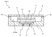
【解決手段】 主面に第1の凹部5を有する基体3と、第1の凹部5内に配設された素子7と、第1の凹部5を封止するように基体3上に配設された蓋体9とを備え、基体3が、素子7の下に位置する部分に第2の凹部11を有し、第2の凹部11の開口部が素子7の下に位置する部分と素子7の周囲に位置する部分とを有していて、第2の凹部11において基体3が素子7から部分的に離隔し、第2の凹部11内に配設されたゲッター材13を更に備えた電子部品1とする。
【選択図】 図1
Description
3・・・基体
3a・・・主面
5・・・第1の凹部
7・・・素子
9・・・蓋体
11・・・第2の凹部
13・・・ゲッター材
15・・・接合部材
17・・・端子
19・・・ヒータ
21・・・パッケージ
23・・・赤外線センサ
25・・・基板
27・・・通電部材
29・・・配線導体
31・・・引出電極
Claims (6)
- 主面に第1の凹部を有する基体と、前記第1の凹部内に配設された素子と、前記第1の凹部を封止するように前記基体上に配設された蓋体とを備えた電子部品であって、前記基体は、前記素子の下に位置する部分に第2の凹部を有し、該第2の凹部を平面視した場合に、前記第2の凹部の開口部が前記素子の下に位置する部分と前記素子の周囲に位置する部分とを有していて、前記第2の凹部において前記基体が前記素子から部分的に離隔しているとともに、前記第2の凹部内に配設されたゲッター材を更に備えていることを特徴とする電子部品。
- 前記ゲッター材と電気的に接続され、前記ゲッター材を通電加熱する端子を更に備えていることを特徴とする請求項1に記載の電子部品。
- 前記基体中の前記ゲッター材の下に位置する部分に埋設されたヒータを更に備えていることを特徴とする請求項1に記載の電子部品。
- 前記第2の凹部の開口部が、前記素子の周囲に位置する部分を複数有していることを特徴とする請求項1に記載の電子部品。
- 主面に素子が配設される第1の凹部を有する基体を備えたパッケージであって、前記基体が前記素子から部分的に離隔するように前記素子の配設領域に第2の凹部を有し、該第2の凹部を平面視した場合に、前記第2の凹部の開口部が前記素子の下に位置する部分と前記素子の周囲に位置する部分とを有していて、前記第2の凹部内に配設されたゲッター材を更に備えていることを特徴とするパッケージ。
- 基板と、該基板上に配設された請求項1に記載の電子部品と、前記素子に通電する通電部材とを備え、前記素子が赤外線センサ素子である赤外線センサ。
Priority Applications (2)
| Application Number | Priority Date | Filing Date | Title |
|---|---|---|---|
| JP2009292213A JP2010251702A (ja) | 2009-03-27 | 2009-12-24 | 電子部品、パッケージおよび赤外線センサ |
| US12/977,695 US20110156190A1 (en) | 2009-03-27 | 2010-12-23 | Electronic component |
Applications Claiming Priority (2)
| Application Number | Priority Date | Filing Date | Title |
|---|---|---|---|
| JP2009079906 | 2009-03-27 | ||
| JP2009292213A JP2010251702A (ja) | 2009-03-27 | 2009-12-24 | 電子部品、パッケージおよび赤外線センサ |
Publications (1)
| Publication Number | Publication Date |
|---|---|
| JP2010251702A true JP2010251702A (ja) | 2010-11-04 |
Family
ID=43313663
Family Applications (1)
| Application Number | Title | Priority Date | Filing Date |
|---|---|---|---|
| JP2009292213A Pending JP2010251702A (ja) | 2009-03-27 | 2009-12-24 | 電子部品、パッケージおよび赤外線センサ |
Country Status (2)
| Country | Link |
|---|---|
| US (1) | US20110156190A1 (ja) |
| JP (1) | JP2010251702A (ja) |
Cited By (6)
| Publication number | Priority date | Publication date | Assignee | Title |
|---|---|---|---|---|
| JP2013195367A (ja) * | 2012-03-22 | 2013-09-30 | Tdk Corp | 赤外線検知装置 |
| JP2013222735A (ja) * | 2012-04-13 | 2013-10-28 | Nec Corp | 赤外線センサパッケージ、赤外線センサモジュール、および電子機器 |
| JP2014090118A (ja) * | 2012-10-31 | 2014-05-15 | Kyocera Corp | イメージセンサ用パッケージおよびイメージセンサ |
| CN103824817A (zh) * | 2013-12-19 | 2014-05-28 | 无锡微奇科技有限公司 | 传感器的真空陶瓷封装结构 |
| WO2018139416A1 (ja) * | 2017-01-26 | 2018-08-02 | 京セラ株式会社 | センサ用配線基板、センサ用パッケージおよびセンサ装置 |
| US10187073B2 (en) | 2015-05-28 | 2019-01-22 | Seiko Epson Corporation | Electronic device, quantum interference device, atomic oscillator, magnetocardiograph, oscillator, electronic apparatus, moving object, and method of manufacturing electronic device |
Families Citing this family (5)
| Publication number | Priority date | Publication date | Assignee | Title |
|---|---|---|---|---|
| WO2006046646A1 (ja) * | 2004-10-27 | 2006-05-04 | Kyocera Corporation | 燃料改質器収納用容器および燃料改質装置 |
| CN102956661B (zh) * | 2012-11-21 | 2016-01-20 | 烟台睿创微纳技术有限公司 | 一种芯片封装方法及其封装结构 |
| CN102956662B (zh) * | 2012-11-22 | 2015-01-28 | 烟台睿创微纳技术有限公司 | 一种红外焦平面探测器芯片真空密封封装结构及封装方法 |
| JP6154458B2 (ja) * | 2013-02-25 | 2017-06-28 | 京セラ株式会社 | 電子部品収納用パッケージおよび電子装置 |
| FR3006236B1 (fr) * | 2013-06-03 | 2016-07-29 | Commissariat Energie Atomique | Procede de collage metallique direct |
Citations (7)
| Publication number | Priority date | Publication date | Assignee | Title |
|---|---|---|---|---|
| JP2003204221A (ja) * | 2001-12-28 | 2003-07-18 | Nippon Dempa Kogyo Co Ltd | 表面実装発振器用容器の製造方法及びこれによる水晶発振器 |
| JP2006513046A (ja) * | 2003-01-17 | 2006-04-20 | サエス ゲッターズ ソチエタ ペル アツィオニ | ゲッター物質のデポジットと組み込まれたヒーターを有するマイクロ機械デバイス又はマイクロオプトエレクトロニック・デバイス、及びその製造のためのサポート |
| US20060189035A1 (en) * | 2004-12-09 | 2006-08-24 | Chien-Hua Chen | Placement of Absorbing Material in a Semiconductor Device |
| JP2007136668A (ja) * | 2005-11-22 | 2007-06-07 | Honeywell Internatl Inc | Memsフリップチップパッケージング |
| JP2007234636A (ja) * | 2006-02-27 | 2007-09-13 | Kyocera Corp | 蓋体およびそれを用いた電子装置 |
| JP2007324466A (ja) * | 2006-06-02 | 2007-12-13 | Nissan Motor Co Ltd | 半導体パッケージ |
| JP2008098262A (ja) * | 2006-10-10 | 2008-04-24 | Matsushita Electric Ind Co Ltd | 半導体装置及び半導体素子搭載用基板の製造方法並びにカメラモジュール |
Family Cites Families (1)
| Publication number | Priority date | Publication date | Assignee | Title |
|---|---|---|---|---|
| WO2005015637A1 (ja) * | 2003-08-08 | 2005-02-17 | Matsushita Electric Industrial Co., Ltd. | 電子デバイスおよびその製造方法 |
-
2009
- 2009-12-24 JP JP2009292213A patent/JP2010251702A/ja active Pending
-
2010
- 2010-12-23 US US12/977,695 patent/US20110156190A1/en not_active Abandoned
Patent Citations (7)
| Publication number | Priority date | Publication date | Assignee | Title |
|---|---|---|---|---|
| JP2003204221A (ja) * | 2001-12-28 | 2003-07-18 | Nippon Dempa Kogyo Co Ltd | 表面実装発振器用容器の製造方法及びこれによる水晶発振器 |
| JP2006513046A (ja) * | 2003-01-17 | 2006-04-20 | サエス ゲッターズ ソチエタ ペル アツィオニ | ゲッター物質のデポジットと組み込まれたヒーターを有するマイクロ機械デバイス又はマイクロオプトエレクトロニック・デバイス、及びその製造のためのサポート |
| US20060189035A1 (en) * | 2004-12-09 | 2006-08-24 | Chien-Hua Chen | Placement of Absorbing Material in a Semiconductor Device |
| JP2007136668A (ja) * | 2005-11-22 | 2007-06-07 | Honeywell Internatl Inc | Memsフリップチップパッケージング |
| JP2007234636A (ja) * | 2006-02-27 | 2007-09-13 | Kyocera Corp | 蓋体およびそれを用いた電子装置 |
| JP2007324466A (ja) * | 2006-06-02 | 2007-12-13 | Nissan Motor Co Ltd | 半導体パッケージ |
| JP2008098262A (ja) * | 2006-10-10 | 2008-04-24 | Matsushita Electric Ind Co Ltd | 半導体装置及び半導体素子搭載用基板の製造方法並びにカメラモジュール |
Cited By (6)
| Publication number | Priority date | Publication date | Assignee | Title |
|---|---|---|---|---|
| JP2013195367A (ja) * | 2012-03-22 | 2013-09-30 | Tdk Corp | 赤外線検知装置 |
| JP2013222735A (ja) * | 2012-04-13 | 2013-10-28 | Nec Corp | 赤外線センサパッケージ、赤外線センサモジュール、および電子機器 |
| JP2014090118A (ja) * | 2012-10-31 | 2014-05-15 | Kyocera Corp | イメージセンサ用パッケージおよびイメージセンサ |
| CN103824817A (zh) * | 2013-12-19 | 2014-05-28 | 无锡微奇科技有限公司 | 传感器的真空陶瓷封装结构 |
| US10187073B2 (en) | 2015-05-28 | 2019-01-22 | Seiko Epson Corporation | Electronic device, quantum interference device, atomic oscillator, magnetocardiograph, oscillator, electronic apparatus, moving object, and method of manufacturing electronic device |
| WO2018139416A1 (ja) * | 2017-01-26 | 2018-08-02 | 京セラ株式会社 | センサ用配線基板、センサ用パッケージおよびセンサ装置 |
Also Published As
| Publication number | Publication date |
|---|---|
| US20110156190A1 (en) | 2011-06-30 |
Similar Documents
| Publication | Publication Date | Title |
|---|---|---|
| JP2010251702A (ja) | 電子部品、パッケージおよび赤外線センサ | |
| JP5997393B2 (ja) | 蓋体、パッケージおよび電子装置 | |
| JP6154458B2 (ja) | 電子部品収納用パッケージおよび電子装置 | |
| JP5078933B2 (ja) | パッケージ及びパッケージの製造方法 | |
| JP2009241030A (ja) | パッケージ、真空容器および反応装置 | |
| JP2010087650A (ja) | 表面実装型圧電振動デバイス | |
| JP4439291B2 (ja) | 圧電振動子収納用パッケージおよび圧電装置 | |
| JP2014090118A (ja) | イメージセンサ用パッケージおよびイメージセンサ | |
| JP2010227920A (ja) | ガス吸着素子形成体、ガス吸着素子の実装方法および真空用パッケージ | |
| JP2008252442A (ja) | 圧電振動デバイスの製造方法 | |
| JP2011203194A (ja) | 赤外線センサ | |
| JP5826113B2 (ja) | 圧電振動素子収納用パッケージおよび圧電装置ならびに多数個取り配線基板 | |
| JP4799211B2 (ja) | 蓋体およびそれを用いた電子装置 | |
| JP6166162B2 (ja) | 蓋体、電子部品収納用パッケージおよび電子装置 | |
| US11056635B2 (en) | Electronic component housing package, electronic device, and electronic module | |
| JP2010056929A (ja) | 圧電部品 | |
| JP2009182806A (ja) | 圧電デバイス及びその製造方法 | |
| JP2005244146A (ja) | 電子部品収納用パッケージおよび電子装置ならびに電子装置の実装構造 | |
| JP2011249660A (ja) | 電子部品 | |
| WO2013172443A1 (ja) | 電子部品及びその製造方法 | |
| JP6175313B2 (ja) | パッケージおよび電子装置 | |
| JP2006005295A (ja) | セラミック素子内部電極の引出し電極及びその製造方法 | |
| JP2006210675A (ja) | 電子部品収納用パッケージ及びそれを用いた電子装置 | |
| JP2001127181A (ja) | 電子部品収納用パッケージ | |
| JP2005183724A (ja) | 電子部品収納用パッケージおよび電子装置 |
Legal Events
| Date | Code | Title | Description |
|---|---|---|---|
| A621 | Written request for application examination |
Free format text: JAPANESE INTERMEDIATE CODE: A621 Effective date: 20120918 |
|
| A977 | Report on retrieval |
Free format text: JAPANESE INTERMEDIATE CODE: A971007 Effective date: 20130125 |
|
| A131 | Notification of reasons for refusal |
Free format text: JAPANESE INTERMEDIATE CODE: A131 Effective date: 20130205 |
|
| A521 | Request for written amendment filed |
Free format text: JAPANESE INTERMEDIATE CODE: A523 Effective date: 20130323 |
|
| A02 | Decision of refusal |
Free format text: JAPANESE INTERMEDIATE CODE: A02 Effective date: 20130702 |