JP2010210824A - 光学素子及び照明装置 - Google Patents
光学素子及び照明装置 Download PDFInfo
- Publication number
- JP2010210824A JP2010210824A JP2009055592A JP2009055592A JP2010210824A JP 2010210824 A JP2010210824 A JP 2010210824A JP 2009055592 A JP2009055592 A JP 2009055592A JP 2009055592 A JP2009055592 A JP 2009055592A JP 2010210824 A JP2010210824 A JP 2010210824A
- Authority
- JP
- Japan
- Prior art keywords
- polarized light
- light
- optical element
- region
- incident
- Prior art date
- Legal status (The legal status is an assumption and is not a legal conclusion. Google has not performed a legal analysis and makes no representation as to the accuracy of the status listed.)
- Withdrawn
Links
Images


Landscapes
- Liquid Crystal (AREA)
- Diffracting Gratings Or Hologram Optical Elements (AREA)
- Polarising Elements (AREA)
Abstract
【解決手段】光Lを基板(入射側基板11)に入射させる入射領域A1と、基板に入射した光Lを第1の方向(X軸方向)に振動する第1の偏光(TM偏光L1)と第1の方向と異なる第2の方向(Y軸方向)に振動する第2の偏光(TE偏光L2)とに分離し、第1の偏光を射出側へ射出させると共に、第2の偏光を回折させる回折領域A2と、回折領域A2で回折された第2の偏光L2を反射させる反射領域A3と、反射領域3で反射された第2の偏光を第1の偏光に変換して射出側へ射出させる位相差領域A4と、を有する。
【選択図】図3
Description
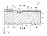
図1は、本実施形態の光学素子の断面構造を部分的に示す模式図である。
入射領域A1における入射側基板11の光の入射側の面11aは平坦になっている。
回折領域A2は、入射領域A1と支持基板10を挟んで対向し、入射領域A1と光の入射方向に重なるように設けられている。回折領域A2における射出側基板12の光の射出側には、回折構造部2とグリッド部3とが設けられている。
グリッド部3は、回折構造部2の表面に設けられている。グリッド部3は、一方向に延在するストライプ状の複数の細線3aにより構成されている。各細線3aは、例えばアルミニウム等の金属材料により形成されている。
図2(A)に示すように、回折構造部2の複数の凸部2aと凹部2bは、一方向(Y軸方向)に延在するストライプ状に設けられている。また、グリッド部3の複数の細線3aは、凸部2a及び凹部2bの延在方向(Y軸方向)に沿って延在するストライプ状に設けられている。
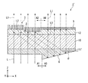
図3に示すように、無偏光の光Lが入射領域A1から入射側基板11に入射すると、入射した光Lは入射側基板11及び支持基板10を透過して射出側基板12の回折領域A2に到達する。回折領域A2に到達した光Lは、回折構造部2及びグリッド部3によりTM偏光L1とTE偏光L2とに分離され、TM偏光L1は光学素子1の外部へ射出され、TE偏光L2は光Lの入射側に反射・回折される。回折領域A2において反射・回折されたTE偏光L2は、支持基板10を透過して入射側基板11の反射領域A3に到達する。
また、位相差領域A4に半波長板5を設けることで、TE偏光L2をTM偏光L1に変換することができる。
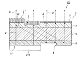
導光板120は、光学素子1のTM偏光L1の射出方向に対して略垂直に設けられ、光学素子1の複数の入射領域A1とTM偏光L1の射出方向に重なるように配置されている。
マイクロレンズアレイ140は、光学素子1の複数の入射領域A1に対応して設けられ、球面側が導光板120に接するように導光板120と光学素子1との間に配置されている。
このように構成することで、第3実施形態の照明装置100と同様に無偏光の入射光Lを一方向に振動するTM偏光L1に効率よく変換して射出することができる。また、導光板120、マイクロレンズアレイ140等を用いる場合と比較して部品点数を削減し、照明装置200をさらに小型化させることができる。これにより、照明装置200を液晶プロジェクターの照明装置として用いることで、液晶プロジェクターの小型化を実現することができる。また、一枚の基板上にアレイ状の回折格子パターンを形成可能であるため、生産性を著しく向上させることができる。
また、回折構造部の一方向に延在する凸部の短手方向の断面形状は、鋸歯状であってもよい。このように凸部の断面形状を鋸歯状にすることで、特定の次数と波長に対して高い回折効率を得ることができる。
また、照明装置は第2実施形態において説明した光学素子を用いたものであってもよい。
また、LED光源と光学素子の入射領域との間にフォトニック結晶を設けてもよい。これによりLED光源の光をより効率よく入射領域へ入射させることができる。
Claims (8)
- 基板の入射側から入射した光を一方向に振動する偏光に変換して前記基板の射出側から射出させる光学素子であって、
前記光を前記基板に入射させる入射領域と、
前記基板に入射した前記光を第1の方向に振動する第1の偏光と前記第1の方向と異なる第2の方向に振動する第2の偏光とに分離し、前記第1の偏光を前記射出側へ射出させると共に、前記第2の偏光を回折させる回折領域と、
前記回折領域で回折された前記第2の偏光を反射させる反射領域と、
前記反射領域で反射された前記第2の偏光を前記第1の偏光に変換して前記射出側へ射出させる位相差領域と、を有する
ことを特徴とする光学素子。 - 前記入射領域と前記反射領域とは前記基板の前記入射側に設けられ、
前記回折領域と前記位相差領域とは前記基板の前記射出側に設けられ、
前記回折領域は、前記第2の偏光を前記入射側に回折させるように設けられ、
前記反射領域は、前記回折領域で回折された前記第2の偏光を前記射出側に反射させるように設けられている
ことを特徴とする請求項1に記載の光学素子。 - 前記回折領域に、一方向に延在する凸部を有する回折構造部と、該回折構造部上に設けられ前記第1の方向と直交する方向に延在する複数の細線を有するグリッド部と、が形成され、
前記光の波長をλ、前記複数の細線の相互間隔をd、前記複数の凸部の相互間隔をδ、前記基板の構成材料の屈折率をnとしたときに、これらのパラメータが、d<λ、かつ、λ/n<δ≦λ、の関係を満たす
ことを特徴とする請求項1又は請求項2に光学素子。 - 前記反射領域に一方向に延在する反射用凸部を有する反射構造部が設けられ、
前記第2の偏光の波長をλ2、前記複数の反射用凸部の相互間隔をδ2、前記基板の構成材料の屈折率をnとしたときに、これらのパラメータが、λ2/n<δ2≦λ2、の関係を満たす
ことを特徴とする請求項1ないし請求項3のいずれか一項に記載の光学素子。 - 前記反射領域に前記第2の偏光を前記射出側へ反射する反射面が形成されている
ことを特徴とする請求項1ないし請求項3のいずれか一項に記載の光学素子。 - 前記位相差領域に半波長板が設けられている
ことを特徴とする請求項1ないし請求項5のいずれか一項に記載の光学素子。 - 請求項1ないし請求項6のいずれか一項に記載の光学素子を備えた照明装置であって、
前記光を射出する光源と、
前記光源から射出された前記光を前記入射領域へ導く導光板と、
前記導光板により導かれた前記光を前記基板へ入射させる複数のレンズと、を有する
ことを特徴とする照明装置。 - 請求項1ないし請求項6のいずれか一項に記載の光学素子を備えた照明装置であって、
前記入射領域に、前記光を射出するLEDが設けられている
ことを特徴とする照明装置。
Priority Applications (1)
| Application Number | Priority Date | Filing Date | Title |
|---|---|---|---|
| JP2009055592A JP2010210824A (ja) | 2009-03-09 | 2009-03-09 | 光学素子及び照明装置 |
Applications Claiming Priority (1)
| Application Number | Priority Date | Filing Date | Title |
|---|---|---|---|
| JP2009055592A JP2010210824A (ja) | 2009-03-09 | 2009-03-09 | 光学素子及び照明装置 |
Publications (2)
| Publication Number | Publication Date |
|---|---|
| JP2010210824A true JP2010210824A (ja) | 2010-09-24 |
| JP2010210824A5 JP2010210824A5 (ja) | 2012-04-12 |
Family
ID=42971078
Family Applications (1)
| Application Number | Title | Priority Date | Filing Date |
|---|---|---|---|
| JP2009055592A Withdrawn JP2010210824A (ja) | 2009-03-09 | 2009-03-09 | 光学素子及び照明装置 |
Country Status (1)
| Country | Link |
|---|---|
| JP (1) | JP2010210824A (ja) |
Cited By (24)
| Publication number | Priority date | Publication date | Assignee | Title |
|---|---|---|---|---|
| JP2012142501A (ja) * | 2011-01-05 | 2012-07-26 | Sony Corp | 固体撮像装置の製造方法、及び、固体撮像装置 |
| EP2894511A1 (en) * | 2014-01-13 | 2015-07-15 | Samsung Electronics Co., Ltd | In-cell polariser, liquid crystal display including it and method of manufacturing the liquid crystal display |
| WO2015129223A1 (ja) * | 2014-02-28 | 2015-09-03 | パナソニックIpマネジメント株式会社 | 発光装置 |
| WO2015129219A1 (ja) * | 2014-02-28 | 2015-09-03 | パナソニックIpマネジメント株式会社 | 発光素子および発光装置 |
| WO2015129222A1 (ja) * | 2014-02-28 | 2015-09-03 | パナソニックIpマネジメント株式会社 | 発光素子および発光装置 |
| WO2015129224A1 (ja) * | 2014-02-28 | 2015-09-03 | パナソニックIpマネジメント株式会社 | 発光装置 |
| WO2015129221A1 (ja) * | 2014-02-28 | 2015-09-03 | パナソニックIpマネジメント株式会社 | 発光素子および発光装置 |
| JP2016033644A (ja) * | 2014-02-28 | 2016-03-10 | パナソニックIpマネジメント株式会社 | 発光素子および発光装置 |
| US9400346B2 (en) | 2014-02-07 | 2016-07-26 | Samsung Display Co., Ltd. | Manufacturing method of reflective polarizer plate and display device including the same |
| US9515239B2 (en) | 2014-02-28 | 2016-12-06 | Panasonic Intellectual Property Management Co., Ltd. | Light-emitting device and light-emitting apparatus |
| US9518215B2 (en) | 2014-02-28 | 2016-12-13 | Panasonic Intellectual Property Management Co., Ltd. | Light-emitting device and light-emitting apparatus |
| US9618697B2 (en) | 2014-02-28 | 2017-04-11 | Panasonic Intellectual Property Management Co., Ltd. | Light directional angle control for light-emitting device and light-emitting apparatus |
| WO2017119400A1 (ja) * | 2016-01-08 | 2017-07-13 | 大日本印刷株式会社 | 回折光学素子、及び光照射装置 |
| JP2017126064A (ja) * | 2016-01-08 | 2017-07-20 | 大日本印刷株式会社 | 回折光学素子、及び光照射装置 |
| US9882100B2 (en) | 2015-08-20 | 2018-01-30 | Panasonic Intellectual Property Management Co., Ltd. | Light-emitting device having surface structure for limiting directional angle of light |
| US9899577B2 (en) | 2015-06-08 | 2018-02-20 | Panasonic Intellectual Property Management Co., Ltd. | Light-emitting apparatus including photoluminescent layer |
| US10031276B2 (en) | 2015-03-13 | 2018-07-24 | Panasonic Intellectual Property Management Co., Ltd. | Display apparatus including photoluminescent layer |
| US10094522B2 (en) | 2016-03-30 | 2018-10-09 | Panasonic Intellectual Property Management Co., Ltd. | Light-emitting device having photoluminescent layer |
| US10115874B2 (en) | 2015-06-08 | 2018-10-30 | Panasonic Intellectual Property Management Co., Ltd. | Light-emitting device including photoluminescent layer |
| US10113712B2 (en) | 2015-03-13 | 2018-10-30 | Panasonic Intellectual Property Management Co., Ltd. | Light-emitting device including photoluminescent layer |
| US10182702B2 (en) | 2015-03-13 | 2019-01-22 | Panasonic Intellectual Property Management Co., Ltd. | Light-emitting apparatus including photoluminescent layer |
| US10359155B2 (en) | 2015-08-20 | 2019-07-23 | Panasonic Intellectual Property Management Co., Ltd. | Light-emitting apparatus |
| USRE49093E1 (en) | 2015-03-13 | 2022-06-07 | Panasonic Intellectual Property Management Co., Ltd. | Light-emitting apparatus including photoluminescent layer |
| CN114815397A (zh) * | 2022-06-20 | 2022-07-29 | 惠科股份有限公司 | 光学膜片及其制备方法、显示装置 |
Citations (5)
| Publication number | Priority date | Publication date | Assignee | Title |
|---|---|---|---|---|
| JP2001083458A (ja) * | 1999-09-08 | 2001-03-30 | Matsushita Electric Ind Co Ltd | 画像表示装置及びその製造方法 |
| JP2002174723A (ja) * | 2000-12-06 | 2002-06-21 | Minolta Co Ltd | 偏光変換光学系および偏光変換素子 |
| US7046441B2 (en) * | 2003-12-31 | 2006-05-16 | Industrial Technology Research Institute | High transmittance sub-wavelength structure polarization module |
| JP2006133275A (ja) * | 2004-11-02 | 2006-05-25 | Sony Corp | 偏光子、液晶パネルおよび投射型表示装置 |
| JP2007033676A (ja) * | 2005-07-25 | 2007-02-08 | Ricoh Co Ltd | 偏光変換光学素子、光変調モジュール及び投射型画像表示装置 |
-
2009
- 2009-03-09 JP JP2009055592A patent/JP2010210824A/ja not_active Withdrawn
Patent Citations (5)
| Publication number | Priority date | Publication date | Assignee | Title |
|---|---|---|---|---|
| JP2001083458A (ja) * | 1999-09-08 | 2001-03-30 | Matsushita Electric Ind Co Ltd | 画像表示装置及びその製造方法 |
| JP2002174723A (ja) * | 2000-12-06 | 2002-06-21 | Minolta Co Ltd | 偏光変換光学系および偏光変換素子 |
| US7046441B2 (en) * | 2003-12-31 | 2006-05-16 | Industrial Technology Research Institute | High transmittance sub-wavelength structure polarization module |
| JP2006133275A (ja) * | 2004-11-02 | 2006-05-25 | Sony Corp | 偏光子、液晶パネルおよび投射型表示装置 |
| JP2007033676A (ja) * | 2005-07-25 | 2007-02-08 | Ricoh Co Ltd | 偏光変換光学素子、光変調モジュール及び投射型画像表示装置 |
Cited By (34)
| Publication number | Priority date | Publication date | Assignee | Title |
|---|---|---|---|---|
| JP2012142501A (ja) * | 2011-01-05 | 2012-07-26 | Sony Corp | 固体撮像装置の製造方法、及び、固体撮像装置 |
| EP2894511A1 (en) * | 2014-01-13 | 2015-07-15 | Samsung Electronics Co., Ltd | In-cell polariser, liquid crystal display including it and method of manufacturing the liquid crystal display |
| CN104777659A (zh) * | 2014-01-13 | 2015-07-15 | 三星电子株式会社 | 单元内偏振器、液晶显示器以及制造液晶显示器的方法 |
| US9696589B2 (en) | 2014-01-13 | 2017-07-04 | Samsung Electronics Co., Ltd. | In-cell polarizer, liquid crystal display including the same, and method of manufacturing liquid crystal display |
| US9400346B2 (en) | 2014-02-07 | 2016-07-26 | Samsung Display Co., Ltd. | Manufacturing method of reflective polarizer plate and display device including the same |
| US9515239B2 (en) | 2014-02-28 | 2016-12-06 | Panasonic Intellectual Property Management Co., Ltd. | Light-emitting device and light-emitting apparatus |
| US9618697B2 (en) | 2014-02-28 | 2017-04-11 | Panasonic Intellectual Property Management Co., Ltd. | Light directional angle control for light-emitting device and light-emitting apparatus |
| WO2015129221A1 (ja) * | 2014-02-28 | 2015-09-03 | パナソニックIpマネジメント株式会社 | 発光素子および発光装置 |
| JP2016033644A (ja) * | 2014-02-28 | 2016-03-10 | パナソニックIpマネジメント株式会社 | 発光素子および発光装置 |
| WO2015129222A1 (ja) * | 2014-02-28 | 2015-09-03 | パナソニックIpマネジメント株式会社 | 発光素子および発光装置 |
| US10012780B2 (en) | 2014-02-28 | 2018-07-03 | Panasonic Intellectual Property Management Co., Ltd. | Light-emitting device including photoluminescent layer |
| US9518215B2 (en) | 2014-02-28 | 2016-12-13 | Panasonic Intellectual Property Management Co., Ltd. | Light-emitting device and light-emitting apparatus |
| WO2015129224A1 (ja) * | 2014-02-28 | 2015-09-03 | パナソニックIpマネジメント株式会社 | 発光装置 |
| WO2015129219A1 (ja) * | 2014-02-28 | 2015-09-03 | パナソニックIpマネジメント株式会社 | 発光素子および発光装置 |
| WO2015129223A1 (ja) * | 2014-02-28 | 2015-09-03 | パナソニックIpマネジメント株式会社 | 発光装置 |
| US9890912B2 (en) | 2014-02-28 | 2018-02-13 | Panasonic Intellectual Property Management Co., Ltd. | Light-emitting apparatus including photoluminescent layer |
| US9880336B2 (en) | 2014-02-28 | 2018-01-30 | Panasonic Intellectual Property Management Co., Ltd. | Light-emitting device including photoluminescent layer |
| US10113712B2 (en) | 2015-03-13 | 2018-10-30 | Panasonic Intellectual Property Management Co., Ltd. | Light-emitting device including photoluminescent layer |
| US10182702B2 (en) | 2015-03-13 | 2019-01-22 | Panasonic Intellectual Property Management Co., Ltd. | Light-emitting apparatus including photoluminescent layer |
| USRE49093E1 (en) | 2015-03-13 | 2022-06-07 | Panasonic Intellectual Property Management Co., Ltd. | Light-emitting apparatus including photoluminescent layer |
| US10031276B2 (en) | 2015-03-13 | 2018-07-24 | Panasonic Intellectual Property Management Co., Ltd. | Display apparatus including photoluminescent layer |
| US10115874B2 (en) | 2015-06-08 | 2018-10-30 | Panasonic Intellectual Property Management Co., Ltd. | Light-emitting device including photoluminescent layer |
| US9899577B2 (en) | 2015-06-08 | 2018-02-20 | Panasonic Intellectual Property Management Co., Ltd. | Light-emitting apparatus including photoluminescent layer |
| US9882100B2 (en) | 2015-08-20 | 2018-01-30 | Panasonic Intellectual Property Management Co., Ltd. | Light-emitting device having surface structure for limiting directional angle of light |
| US10359155B2 (en) | 2015-08-20 | 2019-07-23 | Panasonic Intellectual Property Management Co., Ltd. | Light-emitting apparatus |
| CN108474878A (zh) * | 2016-01-08 | 2018-08-31 | 大日本印刷株式会社 | 衍射光学元件和光照射装置 |
| JP2017126064A (ja) * | 2016-01-08 | 2017-07-20 | 大日本印刷株式会社 | 回折光学素子、及び光照射装置 |
| US10591133B2 (en) | 2016-01-08 | 2020-03-17 | Dai Nippon Printing Co., Ltd. | Diffractive optical element and light irradiation apparatus |
| US10704763B2 (en) | 2016-01-08 | 2020-07-07 | Dai Nippon Printing Co., Ltd. | Diffractive optical element and light irradiation apparatus |
| JP7077524B2 (ja) | 2016-01-08 | 2022-05-31 | 大日本印刷株式会社 | 回折光学素子、及び光照射装置 |
| WO2017119400A1 (ja) * | 2016-01-08 | 2017-07-13 | 大日本印刷株式会社 | 回折光学素子、及び光照射装置 |
| US10094522B2 (en) | 2016-03-30 | 2018-10-09 | Panasonic Intellectual Property Management Co., Ltd. | Light-emitting device having photoluminescent layer |
| CN114815397A (zh) * | 2022-06-20 | 2022-07-29 | 惠科股份有限公司 | 光学膜片及其制备方法、显示装置 |
| US11774803B1 (en) | 2022-06-20 | 2023-10-03 | HKC Corporation Limited | Optical film and preparation method therefor, and display device |
Similar Documents
| Publication | Publication Date | Title |
|---|---|---|
| JP2010210824A (ja) | 光学素子及び照明装置 | |
| JP4475501B2 (ja) | 分光素子、回折格子、複合回折格子、カラー表示装置、および分波器 | |
| US7369186B2 (en) | Polarizing beam splitter featuring stacked grating layers and display including the same | |
| JP4842763B2 (ja) | 光学素子および光学装置 | |
| JP7125640B2 (ja) | 透過型回折格子の製造方法 | |
| JP5737284B2 (ja) | 光学素子、光源装置、および投射型表示装置 | |
| JP5528623B2 (ja) | インコヒーレント化デバイス、およびこれを用いた光学装置 | |
| WO2012067080A1 (ja) | 光源ユニットおよびそれを備えた投射型表示装置 | |
| US7573546B2 (en) | Wire grid polarizer having dual layer structure and method of fabricating the same | |
| EP1160589A1 (en) | Diffractive optical element and optical system having the same | |
| JP5050594B2 (ja) | 分光装置 | |
| JP2010210824A5 (ja) | ||
| WO2013046921A1 (ja) | 偏光子、偏光光学素子、光源および画像表示装置 | |
| JP5461550B2 (ja) | 導光基板およびこれを備えた光学系 | |
| JP2004273203A (ja) | 導光体、およびそれを用いた表示体 | |
| JP2007333957A (ja) | 画像表示装置 | |
| JP2011145360A (ja) | 光学素子、画像生成装置及び画像表示装置 | |
| WO2014010200A1 (ja) | 光学素子、光学装置および表示装置 | |
| JP4537115B2 (ja) | 偏光分離プリズム | |
| JP2008292591A (ja) | 偏光照明装置および投射型画像表示装置 | |
| JP2007114375A (ja) | 光照射装置および液晶表示装置および液晶投射装置 | |
| WO2014013712A1 (ja) | 光学装置およびそれを用いた表示装置 | |
| JP5188524B2 (ja) | 偏光分離素子 | |
| WO2013021766A1 (ja) | 光学素子、照明装置および投射型画像表示装置 | |
| JP4943790B2 (ja) | 偏光変換ユニット、及び画像投影装置 |
Legal Events
| Date | Code | Title | Description |
|---|---|---|---|
| RD04 | Notification of resignation of power of attorney |
Free format text: JAPANESE INTERMEDIATE CODE: A7424 Effective date: 20120130 |
|
| A521 | Written amendment |
Free format text: JAPANESE INTERMEDIATE CODE: A523 Effective date: 20120228 |
|
| A621 | Written request for application examination |
Free format text: JAPANESE INTERMEDIATE CODE: A621 Effective date: 20120228 |
|
| A977 | Report on retrieval |
Free format text: JAPANESE INTERMEDIATE CODE: A971007 Effective date: 20130531 |
|
| A131 | Notification of reasons for refusal |
Free format text: JAPANESE INTERMEDIATE CODE: A131 Effective date: 20130709 |
|
| A761 | Written withdrawal of application |
Free format text: JAPANESE INTERMEDIATE CODE: A761 Effective date: 20130731 |