JP2010103569A - 半導体光素子 - Google Patents
半導体光素子 Download PDFInfo
- Publication number
- JP2010103569A JP2010103569A JP2010024309A JP2010024309A JP2010103569A JP 2010103569 A JP2010103569 A JP 2010103569A JP 2010024309 A JP2010024309 A JP 2010024309A JP 2010024309 A JP2010024309 A JP 2010024309A JP 2010103569 A JP2010103569 A JP 2010103569A
- Authority
- JP
- Japan
- Prior art keywords
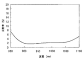
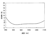
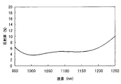
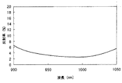
- wavelength
- reflectance
- reflective film
- film
- semiconductor optical
- Prior art date
- Legal status (The legal status is an assumption and is not a legal conclusion. Google has not performed a legal analysis and makes no representation as to the accuracy of the status listed.)
- Pending
Links
Images


Landscapes
- Semiconductor Lasers (AREA)
- Surface Treatment Of Optical Elements (AREA)
Priority Applications (1)
| Application Number | Priority Date | Filing Date | Title |
|---|---|---|---|
| JP2010024309A JP2010103569A (ja) | 2002-09-27 | 2010-02-05 | 半導体光素子 |
Applications Claiming Priority (3)
| Application Number | Priority Date | Filing Date | Title |
|---|---|---|---|
| JP2002283438 | 2002-09-27 | ||
| JP2003057238 | 2003-03-04 | ||
| JP2010024309A JP2010103569A (ja) | 2002-09-27 | 2010-02-05 | 半導体光素子 |
Related Parent Applications (1)
| Application Number | Title | Priority Date | Filing Date |
|---|---|---|---|
| JP2003275554A Division JP2004289108A (ja) | 2002-09-27 | 2003-07-16 | 半導体光素子 |
Publications (1)
| Publication Number | Publication Date |
|---|---|
| JP2010103569A true JP2010103569A (ja) | 2010-05-06 |
Family
ID=42293843
Family Applications (2)
| Application Number | Title | Priority Date | Filing Date |
|---|---|---|---|
| JP2010024309A Pending JP2010103569A (ja) | 2002-09-27 | 2010-02-05 | 半導体光素子 |
| JP2010024313A Pending JP2010123995A (ja) | 2002-09-27 | 2010-02-05 | 半導体光素子 |
Family Applications After (1)
| Application Number | Title | Priority Date | Filing Date |
|---|---|---|---|
| JP2010024313A Pending JP2010123995A (ja) | 2002-09-27 | 2010-02-05 | 半導体光素子 |
Country Status (1)
| Country | Link |
|---|---|
| JP (2) | JP2010103569A (enExample) |
Families Citing this family (2)
| Publication number | Priority date | Publication date | Assignee | Title |
|---|---|---|---|---|
| US20250180783A1 (en) * | 2022-04-14 | 2025-06-05 | Mitsubishi Electric Corporation | Optical semiconductor device and design method for anti-reflection film used in optical semiconductor device |
| JP7378692B1 (ja) * | 2023-07-12 | 2023-11-13 | 三菱電機株式会社 | 光半導体装置の製造方法及び低反射率膜の設計方法 |
Citations (3)
| Publication number | Priority date | Publication date | Assignee | Title |
|---|---|---|---|---|
| JPS62238679A (ja) * | 1986-04-09 | 1987-10-19 | Mitsubishi Electric Corp | 光半導体素子 |
| JPH10186104A (ja) * | 1996-10-24 | 1998-07-14 | Takeshi Kamiya | 多層反射防止膜および光素子 |
| JP2001119096A (ja) * | 1999-10-18 | 2001-04-27 | Fuji Photo Film Co Ltd | 半導体レーザー装置 |
Family Cites Families (1)
| Publication number | Priority date | Publication date | Assignee | Title |
|---|---|---|---|---|
| JP2004289108A (ja) * | 2002-09-27 | 2004-10-14 | Mitsubishi Electric Corp | 半導体光素子 |
-
2010
- 2010-02-05 JP JP2010024309A patent/JP2010103569A/ja active Pending
- 2010-02-05 JP JP2010024313A patent/JP2010123995A/ja active Pending
Patent Citations (3)
| Publication number | Priority date | Publication date | Assignee | Title |
|---|---|---|---|---|
| JPS62238679A (ja) * | 1986-04-09 | 1987-10-19 | Mitsubishi Electric Corp | 光半導体素子 |
| JPH10186104A (ja) * | 1996-10-24 | 1998-07-14 | Takeshi Kamiya | 多層反射防止膜および光素子 |
| JP2001119096A (ja) * | 1999-10-18 | 2001-04-27 | Fuji Photo Film Co Ltd | 半導体レーザー装置 |
Also Published As
| Publication number | Publication date |
|---|---|
| JP2010123995A (ja) | 2010-06-03 |
Similar Documents
| Publication | Publication Date | Title |
|---|---|---|
| JP4097552B2 (ja) | 半導体レーザ装置 | |
| JP2004296903A5 (enExample) | ||
| JP2001119096A (ja) | 半導体レーザー装置 | |
| KR20030074307A (ko) | 광 반도체장치 | |
| JP2010103569A (ja) | 半導体光素子 | |
| JP2004289108A (ja) | 半導体光素子 | |
| CN101841126B (zh) | 多波长半导体激光器和光学记录/再现装置 | |
| KR100598651B1 (ko) | 반도체 레이저장치 | |
| KR100528857B1 (ko) | 반도체 광소자장치 및 그것을 사용한 반도체 레이저 모듈 | |
| JP5941055B2 (ja) | 偏光安定性面発光レーザーダイオード | |
| CN100485986C (zh) | 半导体光电器件 | |
| JP2001196685A (ja) | 半導体光素子装置 | |
| JP5377432B2 (ja) | 半導体光素子装置 | |
| JP3224316B2 (ja) | 二波長反射防止膜 | |
| US6907057B2 (en) | Semiconductor optical device and semiconductor laser module using the semiconductor optical device | |
| JP2006128475A (ja) | 半導体レーザ | |
| JP2010171182A (ja) | 多波長半導体レーザ装置 | |
| JP3194478B2 (ja) | 外部共振器型レーザ装置 | |
| JP4294699B2 (ja) | 半導体レーザ装置 | |
| JP2020031239A5 (enExample) | ||
| JPH0769494B2 (ja) | 光導波路 | |
| JPH02135401A (ja) | ゲルマニウム用反射防止膜 | |
| WO2025031006A1 (zh) | 一种光学元件和相关器件 | |
| JPH02241075A (ja) | 半導体レーザ装置 | |
| JPH06224514A (ja) | 半導体レーザの端面コーティング |
Legal Events
| Date | Code | Title | Description |
|---|---|---|---|
| A621 | Written request for application examination |
Free format text: JAPANESE INTERMEDIATE CODE: A621 Effective date: 20100205 |
|
| A131 | Notification of reasons for refusal |
Free format text: JAPANESE INTERMEDIATE CODE: A131 Effective date: 20110517 |
|
| A521 | Written amendment |
Free format text: JAPANESE INTERMEDIATE CODE: A523 Effective date: 20110713 |
|
| A131 | Notification of reasons for refusal |
Free format text: JAPANESE INTERMEDIATE CODE: A131 Effective date: 20120117 |
|
| A02 | Decision of refusal |
Free format text: JAPANESE INTERMEDIATE CODE: A02 Effective date: 20120522 |