JP2010101874A - 制御信号数量を拡充可能なチップバーンイン装置 - Google Patents
制御信号数量を拡充可能なチップバーンイン装置 Download PDFInfo
- Publication number
- JP2010101874A JP2010101874A JP2008316963A JP2008316963A JP2010101874A JP 2010101874 A JP2010101874 A JP 2010101874A JP 2008316963 A JP2008316963 A JP 2008316963A JP 2008316963 A JP2008316963 A JP 2008316963A JP 2010101874 A JP2010101874 A JP 2010101874A
- Authority
- JP
- Japan
- Prior art keywords
- pins
- input
- clock
- register
- output
- Prior art date
- Legal status (The legal status is an assumption and is not a legal conclusion. Google has not performed a legal analysis and makes no representation as to the accuracy of the status listed.)
- Granted
Links
Images
Landscapes
- Testing Of Individual Semiconductor Devices (AREA)
- Semiconductor Integrated Circuits (AREA)
- Tests Of Electronic Circuits (AREA)
Abstract
【解決手段】コントローラーが第1時間に順に入力インタフェースの四つの第1クロックピンをイネーブルし、入力インタフェース内のデータをバッチごとに四つの第1レジスタの対応入力ピンに出力し並びに暫時保存し、並びに同期して第2レジスタに入力ピンより入力し暫時保存し、コントローラーは更に次の時間に入力インタフェースの第2クロックピンをイネーブルし、第2レジスタ内に保存された全てのデータ信号を出力インタフェースに一次伝送する。こうして入力インタフェース拡充の機能を達成し、既存のハードウエア設備を改修せずにメモリバーンイン装置構造でチップバーンインを可能とし、コストを節約し、快速で、便利な長所を具備するようにした。
【選択図】図2
Description
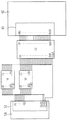
各該第1レジスタ21、22、23、24はN個の入力ピンd1、d2、d3、・・・、dn、クロックピンCLK、及びN個の出力ピンq1、q2、q3、・・・、qnを有する。本実施例では、第1レジスタ21、22、23、24はそれぞれラッチとされる。
21、22、23、24 第1レジスタ 31、32 第2レジスタ
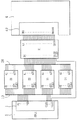
4、42 バーンインボード 40、41 出力インタフェース
5、50 コントローラー 61、62 第1レジスタ
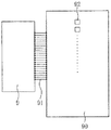
9 インタフェースカード 90 バーンインボード
91 出力ピン 92 メモリチップ
p1、p2、p3、・・・、pn 入力ピン
d1、d2、d3、・・・、dn 入力ピン
D1、D2、D3、・・・、Dm 入力ピン
q1、q2、q3、・・・、qn 出力ピン
Q1、Q2、Q3、・・・、Qm 出力ピン
CLK1、CLK2、CLK3、CLK4 第1クロックピン
T1、T2 時間 DR1、DR2、DR3、・・・、DRm データ出力ピン
CLK5 第2クロックピン I1、I2、I3、I4 バーンインデータ
Claims (5)
- 制御信号数量を拡充可能なチップバーンイン装置において、
第1バスと、
第2バスと、
少なくとも二つの第1レジスタであって、各該第1レジスタはN個の入力ピン、一つのクロックピン、及びN個の出力ピンを有し、そのうち、Nは1以上の正の整数を指し、該N個の入力ピン及び該クロックピンはそれぞれ該第1バスに電気的に接続され、該N個の出力ピンはそれぞれ該第2バスに電気的に接続される、該少なくとも二つの第1レジスタと、
第2レジスタであって、M個の入力ピン、一つのクロックピン、及びM個の出力ピンを有し、そのうち、MはNより大きい正の整数を指し、該M個の入力ピンはそれぞれ該第2バスに電気的に接続され、並びにそれぞれ該少なくとも二つの第1レジスタのそのうち一つの出力ピンに対応して電気的に接続される、該第2レジスタと、
出力インタフェースであって、該第2レジスタのM個の出力ピンにそれぞれ対応し電気的に接続されるM個のデータ出力ピンを有する、該出力インタフェースと、
入力インタフェースであって、該第1バスに電気的に接続され、該入力インタフェースはN個の入力ピン、少なくとも二つの第1クロックピン、及び一つの第2クロックピンを有し、そのうち、該少なくとも二つの第1クロックピンの数量は該少なくとも二つの第1レジスタの数量と同じであり、該少なくとも二つの第1クロックピンはそれぞれ該少なくとも二つの第1レジスタのクロックピンに対応して電気的に接続され、該第2クロックピンは該第2レジスタのクロックピンに対応して電気的に接続される、該入力インタフェースと、
コントローラーであって、まず該入力インタフェースの該少なくとも二つの第1クロックピンをイネーブルした後、更に次の時間に該入力インタフェースの第2クロックピンをイネーブルする、該コントローラーと、
を包含したことを特徴とする、制御信号数量を拡充可能なチップバーンイン装置。 - 請求項1記載の制御信号数量を拡充可能なチップバーンイン装置において、該コントローラーはFPGAチップモジュールを包含することを特徴とする、制御信号数量を拡充可能なチップバーンイン装置。
- 請求項1記載の制御信号数量を拡充可能なチップバーンイン装置において、該コントローラーは順に該入力インタフェースの該少なくとも二つの第1クロックピンをイネーブルし、該入力インタフェースのN個の入力ピンのデータ信号は該第1バスを通してバッチ伝送され、並びに順にイネーブルされた第1クロックピンに対応する第1レジスタのN個の入力ピンを通して暫時保存され、並びに同期して第2ジレスタにその入力ピンを通して暫時保存されることを特徴とする、制御信号数量を拡充可能なチップバーンイン装置。
- 請求項1記載の制御信号数量を拡充可能なチップバーンイン装置において、該コントローラーは該次の時間に該入力インタフェースの該第2クロックピンをイネーブルし、該第2レジスタの該M個の入力ピンにデータ信号を該出力インタフェースの該M個のデータ出力ピンへと出力させることを特徴とする、制御信号数量を拡充可能なチップバーンイン装置。
- 請求項1記載の制御信号数量を拡充可能なチップバーンイン装置において、該正の整数Mは該正の整数Nの整数倍数とされることを特徴とする、制御信号数量を拡充可能なチップバーンイン装置。
Applications Claiming Priority (2)
| Application Number | Priority Date | Filing Date | Title |
|---|---|---|---|
| TW097141249 | 2008-10-27 | ||
| TW97141249A TWI395276B (zh) | 2008-10-27 | 2008-10-27 | Chip can be expanded to control the number of signal burner |
Publications (2)
| Publication Number | Publication Date |
|---|---|
| JP2010101874A true JP2010101874A (ja) | 2010-05-06 |
| JP4870144B2 JP4870144B2 (ja) | 2012-02-08 |
Family
ID=42292634
Family Applications (1)
| Application Number | Title | Priority Date | Filing Date |
|---|---|---|---|
| JP2008316963A Active JP4870144B2 (ja) | 2008-10-27 | 2008-12-12 | 制御信号数量を拡充可能なチップバーンイン装置 |
Country Status (2)
| Country | Link |
|---|---|
| JP (1) | JP4870144B2 (ja) |
| TW (1) | TWI395276B (ja) |
Citations (3)
| Publication number | Priority date | Publication date | Assignee | Title |
|---|---|---|---|---|
| JPS5814547A (ja) * | 1981-07-16 | 1983-01-27 | インタ−ナシヨナル・ビジネス・マシ−ンズ・コ−ポレ−シヨン | 集積回路テスト・システム |
| JPH03267779A (ja) * | 1990-03-16 | 1991-11-28 | Fujitsu Ltd | 集積回路試験装置 |
| JPH06342036A (ja) * | 1993-02-23 | 1994-12-13 | Hewlett Packard Co <Hp> | 電子デバイスの試験装置 |
Family Cites Families (2)
| Publication number | Priority date | Publication date | Assignee | Title |
|---|---|---|---|---|
| US6980016B2 (en) * | 2001-07-02 | 2005-12-27 | Intel Corporation | Integrated circuit burn-in systems |
| US7345495B2 (en) * | 2004-06-30 | 2008-03-18 | Intel Corporation | Temperature and voltage controlled integrated circuit processes |
-
2008
- 2008-10-27 TW TW97141249A patent/TWI395276B/zh active
- 2008-12-12 JP JP2008316963A patent/JP4870144B2/ja active Active
Patent Citations (3)
| Publication number | Priority date | Publication date | Assignee | Title |
|---|---|---|---|---|
| JPS5814547A (ja) * | 1981-07-16 | 1983-01-27 | インタ−ナシヨナル・ビジネス・マシ−ンズ・コ−ポレ−シヨン | 集積回路テスト・システム |
| JPH03267779A (ja) * | 1990-03-16 | 1991-11-28 | Fujitsu Ltd | 集積回路試験装置 |
| JPH06342036A (ja) * | 1993-02-23 | 1994-12-13 | Hewlett Packard Co <Hp> | 電子デバイスの試験装置 |
Also Published As
| Publication number | Publication date |
|---|---|
| TWI395276B (zh) | 2013-05-01 |
| TW201017783A (en) | 2010-05-01 |
| JP4870144B2 (ja) | 2012-02-08 |
Similar Documents
| Publication | Publication Date | Title |
|---|---|---|
| US10281524B2 (en) | Test partition external input/output interface control for test partitions in a semiconductor | |
| US6754863B1 (en) | Scan interface chip (SIC) system and method for scan testing electronic systems | |
| US10628375B2 (en) | Method and system for enumerating digital circuits in a system-on-a-chip (SOC) | |
| CN106526463A (zh) | 具扫描测试的集成电路及其测试方法 | |
| US11519963B2 (en) | Semiconductor integrated circuit having scan chains sequentially supplied with a clock signal | |
| US9264023B2 (en) | Scannable flop with a single storage element | |
| TWI515707B (zh) | 影像顯示系統、移位暫存器與移位暫存器控制方法 | |
| US6760876B1 (en) | Scan interface chip (SIC) system and method for scan testing electronic systems | |
| CN209215538U (zh) | 测试设备与测试系统 | |
| US7958419B2 (en) | Entering a shift-DR state in one of star connected components | |
| CN114490214B (zh) | 一种老化测试接口扩展模块和老化测试系统 | |
| JP4870144B2 (ja) | 制御信号数量を拡充可能なチップバーンイン装置 | |
| US9612280B2 (en) | Partial scan cell | |
| US9448284B2 (en) | Method and apparatus for test time reduction using fractional data packing | |
| CN108463734A (zh) | 用于具有锁存器及触发器的电路设计的扫描逻辑 | |
| US8495436B1 (en) | System and method for memory testing in electronic circuits | |
| US9576620B2 (en) | Semiconductor apparatus and operating method thereof | |
| KR101309182B1 (ko) | 대규모 집적회로 테스터에서 타이밍 발생 및 포맷 장치 | |
| US20140288871A1 (en) | Test apparatus and test system | |
| US7373571B2 (en) | Achieving desired synchronization at sequential elements while testing integrated circuits using sequential scan techniques | |
| CN110489280B (zh) | Usb连接端口测试系统及动态测试usb连接端口的方法 | |
| KR102011139B1 (ko) | 시스템 온 칩의 초기화 장치 | |
| JP2653945B2 (ja) | 半導体集積回路 | |
| CN107015135B (zh) | 自动测试通道配置装置及其控制方法 | |
| US20190080039A1 (en) | Integrated circuit, scan shift control method, and circuit design method |
Legal Events
| Date | Code | Title | Description |
|---|---|---|---|
| A131 | Notification of reasons for refusal |
Free format text: JAPANESE INTERMEDIATE CODE: A131 Effective date: 20110719 |
|
| TRDD | Decision of grant or rejection written | ||
| A01 | Written decision to grant a patent or to grant a registration (utility model) |
Free format text: JAPANESE INTERMEDIATE CODE: A01 Effective date: 20111025 |
|
| A01 | Written decision to grant a patent or to grant a registration (utility model) |
Free format text: JAPANESE INTERMEDIATE CODE: A01 |
|
| A61 | First payment of annual fees (during grant procedure) |
Free format text: JAPANESE INTERMEDIATE CODE: A61 Effective date: 20111116 |
|
| R150 | Certificate of patent or registration of utility model |
Ref document number: 4870144 Country of ref document: JP Free format text: JAPANESE INTERMEDIATE CODE: R150 Free format text: JAPANESE INTERMEDIATE CODE: R150 |
|
| FPAY | Renewal fee payment (event date is renewal date of database) |
Free format text: PAYMENT UNTIL: 20141125 Year of fee payment: 3 |
|
| R250 | Receipt of annual fees |
Free format text: JAPANESE INTERMEDIATE CODE: R250 |
|
| R250 | Receipt of annual fees |
Free format text: JAPANESE INTERMEDIATE CODE: R250 |
|
| R250 | Receipt of annual fees |
Free format text: JAPANESE INTERMEDIATE CODE: R250 |
|
| R250 | Receipt of annual fees |
Free format text: JAPANESE INTERMEDIATE CODE: R250 |
|
| R250 | Receipt of annual fees |
Free format text: JAPANESE INTERMEDIATE CODE: R250 |
|
| R250 | Receipt of annual fees |
Free format text: JAPANESE INTERMEDIATE CODE: R250 |
|
| R250 | Receipt of annual fees |
Free format text: JAPANESE INTERMEDIATE CODE: R250 |
|
| R250 | Receipt of annual fees |
Free format text: JAPANESE INTERMEDIATE CODE: R250 |
|
| R250 | Receipt of annual fees |
Free format text: JAPANESE INTERMEDIATE CODE: R250 |
|
| R250 | Receipt of annual fees |
Free format text: JAPANESE INTERMEDIATE CODE: R250 |
|
| R250 | Receipt of annual fees |
Free format text: JAPANESE INTERMEDIATE CODE: R250 |
|
| R250 | Receipt of annual fees |
Free format text: JAPANESE INTERMEDIATE CODE: R250 |