JP2010055731A - 半導体記憶装置及び情報処理システム - Google Patents
半導体記憶装置及び情報処理システム Download PDFInfo
- Publication number
- JP2010055731A JP2010055731A JP2008222943A JP2008222943A JP2010055731A JP 2010055731 A JP2010055731 A JP 2010055731A JP 2008222943 A JP2008222943 A JP 2008222943A JP 2008222943 A JP2008222943 A JP 2008222943A JP 2010055731 A JP2010055731 A JP 2010055731A
- Authority
- JP
- Japan
- Prior art keywords
- memory cell
- cell array
- memory device
- semiconductor memory
- oxide
- Prior art date
- Legal status (The legal status is an assumption and is not a legal conclusion. Google has not performed a legal analysis and makes no representation as to the accuracy of the status listed.)
- Granted
Links
- 239000004065 semiconductor Substances 0.000 title claims abstract description 57
- 230000010365 information processing Effects 0.000 title claims description 5
- 239000003989 dielectric material Substances 0.000 claims abstract description 11
- 239000000203 mixture Substances 0.000 claims abstract 2
- 239000003990 capacitor Substances 0.000 claims description 22
- 230000008859 change Effects 0.000 claims description 9
- 239000000463 material Substances 0.000 claims description 6
- MRELNEQAGSRDBK-UHFFFAOYSA-N lanthanum(3+);oxygen(2-) Chemical compound [O-2].[O-2].[O-2].[La+3].[La+3] MRELNEQAGSRDBK-UHFFFAOYSA-N 0.000 claims description 4
- 238000012545 processing Methods 0.000 claims description 4
- 229910000314 transition metal oxide Inorganic materials 0.000 claims description 3
- VYPSYNLAJGMNEJ-UHFFFAOYSA-N Silicium dioxide Chemical compound O=[Si]=O VYPSYNLAJGMNEJ-UHFFFAOYSA-N 0.000 claims description 2
- GWEVSGVZZGPLCZ-UHFFFAOYSA-N Titan oxide Chemical group O=[Ti]=O GWEVSGVZZGPLCZ-UHFFFAOYSA-N 0.000 claims description 2
- 229910000449 hafnium oxide Inorganic materials 0.000 claims description 2
- WIHZLLGSGQNAGK-UHFFFAOYSA-N hafnium(4+);oxygen(2-) Chemical compound [O-2].[O-2].[Hf+4] WIHZLLGSGQNAGK-UHFFFAOYSA-N 0.000 claims description 2
- 229910000480 nickel oxide Inorganic materials 0.000 claims description 2
- 229910000484 niobium oxide Inorganic materials 0.000 claims description 2
- URLJKFSTXLNXLG-UHFFFAOYSA-N niobium(5+);oxygen(2-) Chemical compound [O-2].[O-2].[O-2].[O-2].[O-2].[Nb+5].[Nb+5] URLJKFSTXLNXLG-UHFFFAOYSA-N 0.000 claims description 2
- QGLKJKCYBOYXKC-UHFFFAOYSA-N nonaoxidotritungsten Chemical compound O=[W]1(=O)O[W](=O)(=O)O[W](=O)(=O)O1 QGLKJKCYBOYXKC-UHFFFAOYSA-N 0.000 claims description 2
- TWNQGVIAIRXVLR-UHFFFAOYSA-N oxo(oxoalumanyloxy)alumane Chemical compound O=[Al]O[Al]=O TWNQGVIAIRXVLR-UHFFFAOYSA-N 0.000 claims description 2
- SIWVEOZUMHYXCS-UHFFFAOYSA-N oxo(oxoyttriooxy)yttrium Chemical compound O=[Y]O[Y]=O SIWVEOZUMHYXCS-UHFFFAOYSA-N 0.000 claims description 2
- GNRSAWUEBMWBQH-UHFFFAOYSA-N oxonickel Chemical compound [Ni]=O GNRSAWUEBMWBQH-UHFFFAOYSA-N 0.000 claims description 2
- BPUBBGLMJRNUCC-UHFFFAOYSA-N oxygen(2-);tantalum(5+) Chemical compound [O-2].[O-2].[O-2].[O-2].[O-2].[Ta+5].[Ta+5] BPUBBGLMJRNUCC-UHFFFAOYSA-N 0.000 claims description 2
- RVTZCBVAJQQJTK-UHFFFAOYSA-N oxygen(2-);zirconium(4+) Chemical compound [O-2].[O-2].[Zr+4] RVTZCBVAJQQJTK-UHFFFAOYSA-N 0.000 claims description 2
- 229910052814 silicon oxide Inorganic materials 0.000 claims description 2
- 229910001936 tantalum oxide Inorganic materials 0.000 claims description 2
- OGIDPMRJRNCKJF-UHFFFAOYSA-N titanium oxide Inorganic materials [Ti]=O OGIDPMRJRNCKJF-UHFFFAOYSA-N 0.000 claims description 2
- 229910001930 tungsten oxide Inorganic materials 0.000 claims description 2
- 229910001928 zirconium oxide Inorganic materials 0.000 claims description 2
- 230000006870 function Effects 0.000 claims 2
- 238000004519 manufacturing process Methods 0.000 abstract description 9
- 238000000034 method Methods 0.000 description 34
- 230000008569 process Effects 0.000 description 25
- 238000010586 diagram Methods 0.000 description 11
- 230000003071 parasitic effect Effects 0.000 description 10
- 238000003860 storage Methods 0.000 description 9
- 238000009826 distribution Methods 0.000 description 8
- 238000003491 array Methods 0.000 description 7
- 239000010955 niobium Substances 0.000 description 6
- 230000002950 deficient Effects 0.000 description 3
- 238000012360 testing method Methods 0.000 description 3
- 238000012546 transfer Methods 0.000 description 3
- 230000003321 amplification Effects 0.000 description 2
- 230000005540 biological transmission Effects 0.000 description 2
- 230000000694 effects Effects 0.000 description 2
- 238000003199 nucleic acid amplification method Methods 0.000 description 2
- 230000004888 barrier function Effects 0.000 description 1
- 230000015572 biosynthetic process Effects 0.000 description 1
- 238000012790 confirmation Methods 0.000 description 1
- 238000013461 design Methods 0.000 description 1
- 238000013100 final test Methods 0.000 description 1
- 230000012447 hatching Effects 0.000 description 1
- 239000012535 impurity Substances 0.000 description 1
- 238000012986 modification Methods 0.000 description 1
- 230000004048 modification Effects 0.000 description 1
- 230000008439 repair process Effects 0.000 description 1
- 230000000717 retained effect Effects 0.000 description 1
- 239000000523 sample Substances 0.000 description 1
- 238000007789 sealing Methods 0.000 description 1
Images


Classifications
-
- G—PHYSICS
- G11—INFORMATION STORAGE
- G11C—STATIC STORES
- G11C11/00—Digital stores characterised by the use of particular electric or magnetic storage elements; Storage elements therefor
- G11C11/21—Digital stores characterised by the use of particular electric or magnetic storage elements; Storage elements therefor using electric elements
- G11C11/34—Digital stores characterised by the use of particular electric or magnetic storage elements; Storage elements therefor using electric elements using semiconductor devices
- G11C11/40—Digital stores characterised by the use of particular electric or magnetic storage elements; Storage elements therefor using electric elements using semiconductor devices using transistors
- G11C11/401—Digital stores characterised by the use of particular electric or magnetic storage elements; Storage elements therefor using electric elements using semiconductor devices using transistors forming cells needing refreshing or charge regeneration, i.e. dynamic cells
- G11C11/403—Digital stores characterised by the use of particular electric or magnetic storage elements; Storage elements therefor using electric elements using semiconductor devices using transistors forming cells needing refreshing or charge regeneration, i.e. dynamic cells with charge regeneration common to a multiplicity of memory cells, i.e. external refresh
- G11C11/404—Digital stores characterised by the use of particular electric or magnetic storage elements; Storage elements therefor using electric elements using semiconductor devices using transistors forming cells needing refreshing or charge regeneration, i.e. dynamic cells with charge regeneration common to a multiplicity of memory cells, i.e. external refresh with one charge-transfer gate, e.g. MOS transistor, per cell
-
- G—PHYSICS
- G11—INFORMATION STORAGE
- G11C—STATIC STORES
- G11C11/00—Digital stores characterised by the use of particular electric or magnetic storage elements; Storage elements therefor
- G11C11/005—Digital stores characterised by the use of particular electric or magnetic storage elements; Storage elements therefor comprising combined but independently operative RAM-ROM, RAM-PROM, RAM-EPROM cells
-
- G—PHYSICS
- G11—INFORMATION STORAGE
- G11C—STATIC STORES
- G11C11/00—Digital stores characterised by the use of particular electric or magnetic storage elements; Storage elements therefor
- G11C11/21—Digital stores characterised by the use of particular electric or magnetic storage elements; Storage elements therefor using electric elements
- G11C11/34—Digital stores characterised by the use of particular electric or magnetic storage elements; Storage elements therefor using electric elements using semiconductor devices
- G11C11/40—Digital stores characterised by the use of particular electric or magnetic storage elements; Storage elements therefor using electric elements using semiconductor devices using transistors
- G11C11/401—Digital stores characterised by the use of particular electric or magnetic storage elements; Storage elements therefor using electric elements using semiconductor devices using transistors forming cells needing refreshing or charge regeneration, i.e. dynamic cells
- G11C11/4063—Auxiliary circuits, e.g. for addressing, decoding, driving, writing, sensing or timing
- G11C11/407—Auxiliary circuits, e.g. for addressing, decoding, driving, writing, sensing or timing for memory cells of the field-effect type
- G11C11/4076—Timing circuits
-
- G—PHYSICS
- G11—INFORMATION STORAGE
- G11C—STATIC STORES
- G11C13/00—Digital stores characterised by the use of storage elements not covered by groups G11C11/00, G11C23/00, or G11C25/00
- G11C13/0002—Digital stores characterised by the use of storage elements not covered by groups G11C11/00, G11C23/00, or G11C25/00 using resistive RAM [RRAM] elements
- G11C13/0007—Digital stores characterised by the use of storage elements not covered by groups G11C11/00, G11C23/00, or G11C25/00 using resistive RAM [RRAM] elements comprising metal oxide memory material, e.g. perovskites
-
- G—PHYSICS
- G11—INFORMATION STORAGE
- G11C—STATIC STORES
- G11C13/00—Digital stores characterised by the use of storage elements not covered by groups G11C11/00, G11C23/00, or G11C25/00
- G11C13/0002—Digital stores characterised by the use of storage elements not covered by groups G11C11/00, G11C23/00, or G11C25/00 using resistive RAM [RRAM] elements
- G11C13/0021—Auxiliary circuits
- G11C13/0033—Disturbance prevention or evaluation; Refreshing of disturbed memory data
-
- G—PHYSICS
- G11—INFORMATION STORAGE
- G11C—STATIC STORES
- G11C13/00—Digital stores characterised by the use of storage elements not covered by groups G11C11/00, G11C23/00, or G11C25/00
- G11C13/0002—Digital stores characterised by the use of storage elements not covered by groups G11C11/00, G11C23/00, or G11C25/00 using resistive RAM [RRAM] elements
- G11C13/0021—Auxiliary circuits
- G11C13/0069—Writing or programming circuits or methods
- G11C2013/0083—Write to perform initialising, forming process, electro forming or conditioning
-
- G—PHYSICS
- G11—INFORMATION STORAGE
- G11C—STATIC STORES
- G11C13/00—Digital stores characterised by the use of storage elements not covered by groups G11C11/00, G11C23/00, or G11C25/00
- G11C13/0002—Digital stores characterised by the use of storage elements not covered by groups G11C11/00, G11C23/00, or G11C25/00 using resistive RAM [RRAM] elements
- G11C13/0021—Auxiliary circuits
- G11C13/0069—Writing or programming circuits or methods
- G11C2013/009—Write using potential difference applied between cell electrodes
-
- G—PHYSICS
- G11—INFORMATION STORAGE
- G11C—STATIC STORES
- G11C2213/00—Indexing scheme relating to G11C13/00 for features not covered by this group
- G11C2213/30—Resistive cell, memory material aspects
- G11C2213/32—Material having simple binary metal oxide structure
Landscapes
- Engineering & Computer Science (AREA)
- Microelectronics & Electronic Packaging (AREA)
- Computer Hardware Design (AREA)
- Chemical & Material Sciences (AREA)
- Materials Engineering (AREA)
- Dram (AREA)
- Semiconductor Memories (AREA)
Abstract
【解決手段】本発明の半導体記憶装置のメモリセルアレイには、誘電体材料を2つの電極で挟んだ構造をそれぞれ有する複数の第1メモリセルMCがアレイ状に配置され、指定可能な複数の領域に区分されている。メモリセルアレイの中から選択的に指定された領域において第1メモリセルMCに対するフォーミングが実行され、不揮発性の第2メモリセルMCaに変更される。これにより、DRAMメモリセルアレイと不揮発性のRRAMメモリセルアレイを混載し、製造後に任意に領域を設定可能な半導体記憶装置を実現することができる。
【選択図】図2
Description
2…メディアプロセッサ
3…SIP
4…ベースバンドプロセッサ
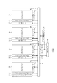
10…メモリセルアレイ
11…グローバルセンスアンプ列
12…カラムデコーダ
13…ロウデコーダ
14…制御回路
15…アレイ情報記憶部
16…入出力ポート
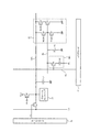
20…センスアンプ
21…グローバルセンスアンプ
WL…ワード線
BL…ビット線
GBL…グローバルビット線
PL…共通プレート線
MC、MCa…メモリセル
Q0…選択NMOSトランジスタ
C0…キャパシタ
RM…抵抗素子
Q1〜Q7…NMOSトランジスタ
PC…プリチャージ信号
RE、WE…制御信号
YS…カラム選択信号
SL…ワード線全選択信号
VDD…電源電圧
VSS…グランド電位
VPP…正電圧
Claims (9)
- 誘電体材料を2つの電極で挟んだ構造をそれぞれ有する複数の第1メモリセルがアレイ状に配置され、指定可能な複数の領域に区分されたメモリセルアレイと、
前記メモリセルアレイの前記複数の領域から選択的に指定された領域において、各々の前記第1メモリセルに対するフォーミングを実行して不揮発性の第2メモリセルに変更するように制御するフォーミング制御部と、
を備えることを特徴とする半導体記憶装置。 - 前記第1メモリセルに対するフォーミングに際し、前記2つの電極の間に所定の電圧を印加することにより前記誘電体材料に導電性パスが形成されることを特徴とする請求項1に記載の半導体記憶装置。
- 前記第1メモリセルは、蓄積電荷に応じて情報を保持するキャパシタを有し、前記第2メモリセルは、抵抗値の大小に応じて情報を保持する抵抗素子を有することを特徴とする請求項1又は2に記載の半導体記憶装置。
- 前記第1メモリセルが配置された領域はDRAMメモリセルアレイとして機能し、前記フォーミングにより前記第1メモリセルが前記第2メモリセルに変更された領域は不揮発性のRRAMメモリセルアレイとして機能することを特徴とする請求項3に記載の半導体記憶装置。
- 前記第1メモリセル又は前記第2メモリセルから読み出されてビット線に伝送される信号を増幅するセンスアンプ回路をさらに備え、前記センスアンプ回路は、前記DRAMメモリセルアレイと前記RRAMメモリセルアレイの両方に対して共用されることを特徴とする請求項4に記載の半導体記憶装置。
- 前記誘電体材料として、遷移金属酸化物、アルミニウム酸化物、シリコン酸化物のいずれか、あるいはそれらの混合材料が用いられることを特徴とする請求項1に記載の半導体記憶装置。
- 前記遷移金属酸化物が、チタン酸化物、ニッケル酸化物、イットリウム酸化物、ジルコニウム酸化物、ニオブ酸化物、ランタン酸化物、ハフニウム酸化物、タンタル酸化物、タングステン酸化物のいずれか、あるいはそれらの混合材料を含むことを特徴とする請求項6に記載の半導体記憶装置。
- 請求項1に記載の半導体記憶装置と、前記半導体装置に記憶された情報を用いて処理を実行するプロセッサとを備えることを特徴とする情報処理システム。
- 前記選択的に指定された領域における前記フォーミングは、前記半導体記憶装置のシステム搭載後に実行されることを特徴とする請求項8に記載の情報処理システム。
Priority Applications (2)
| Application Number | Priority Date | Filing Date | Title |
|---|---|---|---|
| JP2008222943A JP5451011B2 (ja) | 2008-08-29 | 2008-08-29 | 半導体記憶装置及び情報処理システム |
| US12/549,124 US7995373B2 (en) | 2008-08-29 | 2009-08-27 | Semiconductor memory device and information processing system |
Applications Claiming Priority (1)
| Application Number | Priority Date | Filing Date | Title |
|---|---|---|---|
| JP2008222943A JP5451011B2 (ja) | 2008-08-29 | 2008-08-29 | 半導体記憶装置及び情報処理システム |
Publications (2)
| Publication Number | Publication Date |
|---|---|
| JP2010055731A true JP2010055731A (ja) | 2010-03-11 |
| JP5451011B2 JP5451011B2 (ja) | 2014-03-26 |
Family
ID=41725241
Family Applications (1)
| Application Number | Title | Priority Date | Filing Date |
|---|---|---|---|
| JP2008222943A Expired - Fee Related JP5451011B2 (ja) | 2008-08-29 | 2008-08-29 | 半導体記憶装置及び情報処理システム |
Country Status (2)
| Country | Link |
|---|---|
| US (1) | US7995373B2 (ja) |
| JP (1) | JP5451011B2 (ja) |
Cited By (2)
| Publication number | Priority date | Publication date | Assignee | Title |
|---|---|---|---|---|
| US8934283B2 (en) | 2011-09-26 | 2015-01-13 | Renesas Electronics Corporation | Semiconductor memory device, semiconductor device and method of manufacturing semiconductor memory device |
| JP2023118092A (ja) * | 2022-02-11 | 2023-08-24 | イーメモリー テクノロジー インコーポレイテッド | 抵抗変化型メモリセルおよび関連するセルアレイ構造 |
Families Citing this family (2)
| Publication number | Priority date | Publication date | Assignee | Title |
|---|---|---|---|---|
| US9355734B2 (en) * | 2014-03-04 | 2016-05-31 | Silicon Storage Technology, Inc. | Sensing circuits for use in low power nanometer flash memory devices |
| US10643700B2 (en) * | 2015-10-29 | 2020-05-05 | Micron Technology, Inc. | Apparatuses and methods for adjusting write parameters based on a write count |
Citations (6)
| Publication number | Priority date | Publication date | Assignee | Title |
|---|---|---|---|---|
| JPH098247A (ja) * | 1995-06-15 | 1997-01-10 | Hitachi Ltd | 半導体記憶装置 |
| JPH0950700A (ja) * | 1995-06-01 | 1997-02-18 | Sony Corp | 半導体記憶装置 |
| JP2004296076A (ja) * | 2003-03-27 | 2004-10-21 | Samsung Electronics Co Ltd | 不揮発性メモリ及び揮発性メモリで選択的に動作可能な相変化メモリ装置及び相変化メモリ装置の動作方法 |
| JP2007515026A (ja) * | 2003-12-18 | 2007-06-07 | 松下電器産業株式会社 | 抵抗変化材料の初期化方法、抵抗変化材料を用いた記憶素子、可変抵抗体を用いた不揮発性メモリ回路を初期化する方法 |
| JP2008204581A (ja) * | 2007-02-22 | 2008-09-04 | Elpida Memory Inc | 不揮発性ram |
| JP2009087490A (ja) * | 2007-10-01 | 2009-04-23 | Spansion Llc | 半導体装置及びその制御方法 |
Family Cites Families (8)
| Publication number | Priority date | Publication date | Assignee | Title |
|---|---|---|---|---|
| DE69315125T2 (de) * | 1992-06-18 | 1998-06-10 | Matsushita Electronics Corp | Herstellungsverfahren für Halbleiterbauelement mit Kondensator |
| JPH0794681A (ja) | 1993-09-24 | 1995-04-07 | Hitachi Ltd | 酸化物電極 |
| US5675547A (en) * | 1995-06-01 | 1997-10-07 | Sony Corporation | One time programmable read only memory programmed by destruction of insulating layer |
| JPH0982914A (ja) | 1995-09-18 | 1997-03-28 | Fujitsu Ltd | 半導体装置およびその製造方法 |
| JP3622304B2 (ja) * | 1995-12-27 | 2005-02-23 | 株式会社日立製作所 | 半導体記憶装置 |
| JPH11144473A (ja) * | 1997-11-12 | 1999-05-28 | Mitsubishi Electric Corp | 半導体記憶装置 |
| US6665207B2 (en) * | 2001-11-14 | 2003-12-16 | Micron Technology, Inc. | ROM embedded DRAM with dielectric removal/short |
| US6735108B2 (en) * | 2002-07-08 | 2004-05-11 | Micron Technology, Inc. | ROM embedded DRAM with anti-fuse programming |
-
2008
- 2008-08-29 JP JP2008222943A patent/JP5451011B2/ja not_active Expired - Fee Related
-
2009
- 2009-08-27 US US12/549,124 patent/US7995373B2/en not_active Expired - Fee Related
Patent Citations (6)
| Publication number | Priority date | Publication date | Assignee | Title |
|---|---|---|---|---|
| JPH0950700A (ja) * | 1995-06-01 | 1997-02-18 | Sony Corp | 半導体記憶装置 |
| JPH098247A (ja) * | 1995-06-15 | 1997-01-10 | Hitachi Ltd | 半導体記憶装置 |
| JP2004296076A (ja) * | 2003-03-27 | 2004-10-21 | Samsung Electronics Co Ltd | 不揮発性メモリ及び揮発性メモリで選択的に動作可能な相変化メモリ装置及び相変化メモリ装置の動作方法 |
| JP2007515026A (ja) * | 2003-12-18 | 2007-06-07 | 松下電器産業株式会社 | 抵抗変化材料の初期化方法、抵抗変化材料を用いた記憶素子、可変抵抗体を用いた不揮発性メモリ回路を初期化する方法 |
| JP2008204581A (ja) * | 2007-02-22 | 2008-09-04 | Elpida Memory Inc | 不揮発性ram |
| JP2009087490A (ja) * | 2007-10-01 | 2009-04-23 | Spansion Llc | 半導体装置及びその制御方法 |
Cited By (3)
| Publication number | Priority date | Publication date | Assignee | Title |
|---|---|---|---|---|
| US8934283B2 (en) | 2011-09-26 | 2015-01-13 | Renesas Electronics Corporation | Semiconductor memory device, semiconductor device and method of manufacturing semiconductor memory device |
| JP2023118092A (ja) * | 2022-02-11 | 2023-08-24 | イーメモリー テクノロジー インコーポレイテッド | 抵抗変化型メモリセルおよび関連するセルアレイ構造 |
| US12507420B2 (en) | 2022-02-11 | 2025-12-23 | Ememory Technology Inc. | Resistive memory cell and associated cell array structure |
Also Published As
| Publication number | Publication date |
|---|---|
| JP5451011B2 (ja) | 2014-03-26 |
| US7995373B2 (en) | 2011-08-09 |
| US20100054018A1 (en) | 2010-03-04 |
Similar Documents
| Publication | Publication Date | Title |
|---|---|---|
| US7596014B2 (en) | Semiconductor device | |
| CN109690680B (zh) | 包含二晶体管一电容器的存储器及用于存取所述存储器的设备与方法 | |
| US8559253B2 (en) | Variable-resistance memory device with charge sharing that discharges pre-charge voltage of a selected bit line to share charge with unselected bit lines | |
| US10783976B2 (en) | Antifuse memory device and operation method thereof | |
| CN1838321B (zh) | 有增强的位线和/或字线驱动能力的非易失性存储器设备 | |
| JP5222619B2 (ja) | 半導体装置 | |
| US7660148B2 (en) | Nonvolatile memory device and method to control the same | |
| JP2009026382A (ja) | 半導体記憶装置 | |
| CN101877241B (zh) | 半导体存储设备 | |
| US9153625B2 (en) | Non-volatile semiconductor memory device | |
| TW202301334A (zh) | 記憶體元件、感測放大器系統及其控制方法 | |
| US9177637B1 (en) | Wide voltage range high performance sense amplifier | |
| US20150070971A1 (en) | Resistance change memory | |
| JP5451011B2 (ja) | 半導体記憶装置及び情報処理システム | |
| KR20210080581A (ko) | 작은 페이지 버퍼를 이용한 높은 대역폭 동작을 위한 교차점 메모리 아키텍처 | |
| CN100541659C (zh) | 具有2t存储器单元的存储器阵列 | |
| JP2011054233A (ja) | 半導体記憶装置 | |
| JP2013140667A (ja) | 半導体装置 | |
| JP2019046514A (ja) | 半導体記憶装置 | |
| US20070279967A1 (en) | High density magnetic memory cell layout for spin transfer torque magnetic memories utilizing donut shaped transistors | |
| CN110136760B (zh) | Mram芯片 | |
| TW202247184A (zh) | 記憶體裝置 | |
| US20180122461A1 (en) | Resistive memory apparatus | |
| JP2023179834A (ja) | 半導体装置 | |
| JP5293795B2 (ja) | 半導体装置 |
Legal Events
| Date | Code | Title | Description |
|---|---|---|---|
| A621 | Written request for application examination |
Free format text: JAPANESE INTERMEDIATE CODE: A621 Effective date: 20110609 |
|
| A711 | Notification of change in applicant |
Free format text: JAPANESE INTERMEDIATE CODE: A711 Effective date: 20130730 |
|
| A977 | Report on retrieval |
Free format text: JAPANESE INTERMEDIATE CODE: A971007 Effective date: 20131111 |
|
| TRDD | Decision of grant or rejection written | ||
| A01 | Written decision to grant a patent or to grant a registration (utility model) |
Free format text: JAPANESE INTERMEDIATE CODE: A01 Effective date: 20131210 |
|
| A61 | First payment of annual fees (during grant procedure) |
Free format text: JAPANESE INTERMEDIATE CODE: A61 Effective date: 20131226 |
|
| R150 | Certificate of patent or registration of utility model |
Free format text: JAPANESE INTERMEDIATE CODE: R150 |
|
| LAPS | Cancellation because of no payment of annual fees |