JP2010045085A - 積層セラミック・コンデンサのプリント配線基板における配置構造 - Google Patents
積層セラミック・コンデンサのプリント配線基板における配置構造 Download PDFInfo
- Publication number
- JP2010045085A JP2010045085A JP2008206521A JP2008206521A JP2010045085A JP 2010045085 A JP2010045085 A JP 2010045085A JP 2008206521 A JP2008206521 A JP 2008206521A JP 2008206521 A JP2008206521 A JP 2008206521A JP 2010045085 A JP2010045085 A JP 2010045085A
- Authority
- JP
- Japan
- Prior art keywords
- multilayer ceramic
- axis
- capacitor
- ceramic capacitor
- arrangement structure
- Prior art date
- Legal status (The legal status is an assumption and is not a legal conclusion. Google has not performed a legal analysis and makes no representation as to the accuracy of the status listed.)
- Granted
Links
Images


Classifications
-
- H—ELECTRICITY
- H05—ELECTRIC TECHNIQUES NOT OTHERWISE PROVIDED FOR
- H05K—PRINTED CIRCUITS; CASINGS OR CONSTRUCTIONAL DETAILS OF ELECTRIC APPARATUS; MANUFACTURE OF ASSEMBLAGES OF ELECTRICAL COMPONENTS
- H05K1/00—Printed circuits
- H05K1/02—Details
- H05K1/0213—Electrical arrangements not otherwise provided for
- H05K1/0216—Reduction of cross-talk, noise or electromagnetic interference
- H05K1/023—Reduction of cross-talk, noise or electromagnetic interference using auxiliary mounted passive components or auxiliary substances
- H05K1/0231—Capacitors or dielectric substances
-
- H—ELECTRICITY
- H05—ELECTRIC TECHNIQUES NOT OTHERWISE PROVIDED FOR
- H05K—PRINTED CIRCUITS; CASINGS OR CONSTRUCTIONAL DETAILS OF ELECTRIC APPARATUS; MANUFACTURE OF ASSEMBLAGES OF ELECTRICAL COMPONENTS
- H05K1/00—Printed circuits
- H05K1/02—Details
- H05K1/11—Printed elements for providing electric connections to or between printed circuits
- H05K1/111—Pads for surface mounting, e.g. lay-out
-
- H—ELECTRICITY
- H05—ELECTRIC TECHNIQUES NOT OTHERWISE PROVIDED FOR
- H05K—PRINTED CIRCUITS; CASINGS OR CONSTRUCTIONAL DETAILS OF ELECTRIC APPARATUS; MANUFACTURE OF ASSEMBLAGES OF ELECTRICAL COMPONENTS
- H05K1/00—Printed circuits
- H05K1/18—Printed circuits structurally associated with non-printed electric components
- H05K1/181—Printed circuits structurally associated with non-printed electric components associated with surface mounted components
-
- H—ELECTRICITY
- H05—ELECTRIC TECHNIQUES NOT OTHERWISE PROVIDED FOR
- H05K—PRINTED CIRCUITS; CASINGS OR CONSTRUCTIONAL DETAILS OF ELECTRIC APPARATUS; MANUFACTURE OF ASSEMBLAGES OF ELECTRICAL COMPONENTS
- H05K2201/00—Indexing scheme relating to printed circuits covered by H05K1/00
- H05K2201/09—Shape and layout
- H05K2201/09209—Shape and layout details of conductors
- H05K2201/09372—Pads and lands
- H05K2201/09418—Special orientation of pads, lands or terminals of component, e.g. radial or polygonal orientation
-
- H—ELECTRICITY
- H05—ELECTRIC TECHNIQUES NOT OTHERWISE PROVIDED FOR
- H05K—PRINTED CIRCUITS; CASINGS OR CONSTRUCTIONAL DETAILS OF ELECTRIC APPARATUS; MANUFACTURE OF ASSEMBLAGES OF ELECTRICAL COMPONENTS
- H05K2201/00—Indexing scheme relating to printed circuits covered by H05K1/00
- H05K2201/10—Details of components or other objects attached to or integrated in a printed circuit board
- H05K2201/10431—Details of mounted components
- H05K2201/10507—Involving several components
- H05K2201/10522—Adjacent components
-
- H—ELECTRICITY
- H05—ELECTRIC TECHNIQUES NOT OTHERWISE PROVIDED FOR
- H05K—PRINTED CIRCUITS; CASINGS OR CONSTRUCTIONAL DETAILS OF ELECTRIC APPARATUS; MANUFACTURE OF ASSEMBLAGES OF ELECTRICAL COMPONENTS
- H05K2201/00—Indexing scheme relating to printed circuits covered by H05K1/00
- H05K2201/10—Details of components or other objects attached to or integrated in a printed circuit board
- H05K2201/10613—Details of electrical connections of non-printed components, e.g. special leads
- H05K2201/10621—Components characterised by their electrical contacts
- H05K2201/10636—Leadless chip, e.g. chip capacitor or resistor
-
- Y—GENERAL TAGGING OF NEW TECHNOLOGICAL DEVELOPMENTS; GENERAL TAGGING OF CROSS-SECTIONAL TECHNOLOGIES SPANNING OVER SEVERAL SECTIONS OF THE IPC; TECHNICAL SUBJECTS COVERED BY FORMER USPC CROSS-REFERENCE ART COLLECTIONS [XRACs] AND DIGESTS
- Y02—TECHNOLOGIES OR APPLICATIONS FOR MITIGATION OR ADAPTATION AGAINST CLIMATE CHANGE
- Y02P—CLIMATE CHANGE MITIGATION TECHNOLOGIES IN THE PRODUCTION OR PROCESSING OF GOODS
- Y02P70/00—Climate change mitigation technologies in the production process for final industrial or consumer products
- Y02P70/50—Manufacturing or production processes characterised by the final manufactured product
Landscapes
- Physics & Mathematics (AREA)
- Electromagnetism (AREA)
- Engineering & Computer Science (AREA)
- Microelectronics & Electronic Packaging (AREA)
- Structures For Mounting Electric Components On Printed Circuit Boards (AREA)
- Ceramic Capacitors (AREA)
Abstract
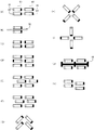
【解決手段】単位配置構造100は、4個の積層セラミック・コンデンサ101、103、105、107で構成される。4個の積層セラミック・コンデンサの中で、2個の積層セラミック・コンデンサ101、103は軸201にコンデンサ軸が沿うように配置され、他の2個の積層セラミック・コンデンサ105、107は軸201と交差する軸203にコンデンサ軸が沿うように配置される。このような配置構造によれば片面実装でも効果的に騒音を抑制することができる。
【選択図】図4
Description
50…プリント配線基板
51a、51b…外部端子
60…コンデンサ軸
61、63、71、73、75、77…配列軸
100…単位配置構造
201、203…単位配置構造の軸
Claims (11)
- プリント配線基板に実装された積層セラミック・コンデンサの単位配置構造であって、
第1の軸にコンデンサ軸が沿うように配置された第1の積層セラミック・コンデンサと、
前記第1の軸にコンデンサ軸が沿うように配置された第2の積層セラミック・コンデンサと、
前記第1の軸と交差する第2の軸にコンデンサ軸が沿うように配置された第3の積層セラミック・コンデンサと、
前記第2の軸にコンデンサ軸が沿うように配置された第4の積層セラミック・コンデンサとを有し、
前記第1の軸と前記第2の軸が交差する位置の近辺で、前記第1の積層セラミック・コンデンサと前記第3の積層セラミック・コンデンサの外部端子同士が前記プリント配線基板のパターンを経由して接続され前記第2の積層セラミック・コンデンサと前記第4の積層セラミック・コンデンサの外部端子同士が前記プリント配線基板のパターンを経由して接続された単位配置構造。 - 前記第1の軸と前記第2の軸が直交している請求項1に記載の単位配置構造。
- 前記第1の積層セラミック・コンデンサ、前記第2の積層セラミック・コンデンサ、前記第3の積層セラミック・コンデンサおよび前記第4の積層セラミック・コンデンサの外形寸法がほぼ同一であり、前記第1の積層セラミック・コンデンサと前記第2の積層セラミック・コンデンサの間隔および前記第3の積層セラミック・コンデンサと前記第4の積層セラミック・コンデンサの間隔がそれぞれ各積層セラミック・コンデンサのコンデンサ軸方向の長さより短い請求項1または請求項2に記載の単位配置構造。
- 前記第1の積層セラミック・コンデンサ、前記第2の積層セラミック・コンデンサ、前記第3の積層セラミック・コンデンサ、および前記第4の積層セラミック・コンデンサが前記プリント配線基板の表面と裏面に配置されている請求項1ないし請求項3のいずれかに記載の単位配置構造。
- 請求項1ないし請求項3のいずれかに記載された前記単位配置構造の前記第1の軸または前記第2の軸が配列軸に沿うようにプリント配線基板に複数の前記単位配置構造が配置された積層セラミック・コンデンサの全体配置構造。
- 前記単位配置構造がほぼ等間隔で配置されている請求項5に記載の全体配置構造。
- 前記全体配置構造が前記プリント配線基板の表面と裏面に配置されている請求項5または請求項6に記載の全体配置構造。
- 請求項1ないし請求項3のいずれかに記載された前記単位配置構造の前記第1の軸と前記第2の軸の2等分線が配列軸に沿うようにプリント配線基板に複数の前記単位配置構造が配置された積層セラミック・コンデンサの全体配置構造。
- 前記単位配置構造がほぼ等間隔で配置されている請求項8に記載の全体配置構造。
- 前記全体配置構造が前記プリント配線基板の表面と裏面に配置されている請求項8または請求項9に記載の全体配置構造。
- 請求項5ないし請求項10のいずれかに記載された全体配置構造で複数の積層セラミック・コンデンサが実装されたプリント配線基板。
Priority Applications (2)
| Application Number | Priority Date | Filing Date | Title |
|---|---|---|---|
| JP2008206521A JP5133813B2 (ja) | 2008-08-11 | 2008-08-11 | 積層セラミック・コンデンサの単位配置構造、全体配置構造およびプリント配線基板 |
| US12/538,399 US8564966B2 (en) | 2008-08-11 | 2009-08-10 | Apparatus for reducing capacitor generated noise on a printed circuit board |
Applications Claiming Priority (1)
| Application Number | Priority Date | Filing Date | Title |
|---|---|---|---|
| JP2008206521A JP5133813B2 (ja) | 2008-08-11 | 2008-08-11 | 積層セラミック・コンデンサの単位配置構造、全体配置構造およびプリント配線基板 |
Publications (2)
| Publication Number | Publication Date |
|---|---|
| JP2010045085A true JP2010045085A (ja) | 2010-02-25 |
| JP5133813B2 JP5133813B2 (ja) | 2013-01-30 |
Family
ID=41652758
Family Applications (1)
| Application Number | Title | Priority Date | Filing Date |
|---|---|---|---|
| JP2008206521A Active JP5133813B2 (ja) | 2008-08-11 | 2008-08-11 | 積層セラミック・コンデンサの単位配置構造、全体配置構造およびプリント配線基板 |
Country Status (2)
| Country | Link |
|---|---|
| US (1) | US8564966B2 (ja) |
| JP (1) | JP5133813B2 (ja) |
Cited By (9)
| Publication number | Priority date | Publication date | Assignee | Title |
|---|---|---|---|---|
| JP2014207381A (ja) * | 2013-04-15 | 2014-10-30 | 株式会社ケーヒン | 直列回路装置 |
| KR20140133465A (ko) * | 2013-05-10 | 2014-11-19 | 가부시키가이샤 무라타 세이사쿠쇼 | 콘덴서 소자의 실장 구조체 및 콘덴서 소자의 실장방법 |
| US9318260B2 (en) | 2013-10-01 | 2016-04-19 | Murata Manufacturing Co., Ltd. | Capacitor-mounted structure and capacitor |
| JP2016105453A (ja) * | 2014-09-01 | 2016-06-09 | 株式会社村田製作所 | 電子部品内蔵基板 |
| KR20180054467A (ko) | 2016-11-15 | 2018-05-24 | 가부시키가이샤 무라타 세이사쿠쇼 | 적층 세라믹 전자부품 |
| US10186377B2 (en) | 2015-02-13 | 2019-01-22 | Murata Manufacturing Co., Ltd. | Multilayer capacitor |
| KR20190116185A (ko) * | 2019-09-20 | 2019-10-14 | 삼성전기주식회사 | 전자 부품 |
| CN111326340A (zh) * | 2020-03-27 | 2020-06-23 | 无锡赛晶电力电容器有限公司 | 一种有效降低电容器组噪声的布置结构 |
| EP3809806A1 (en) | 2019-10-18 | 2021-04-21 | Ricoh Company, Ltd. | Wiring board |
Families Citing this family (17)
| Publication number | Priority date | Publication date | Assignee | Title |
|---|---|---|---|---|
| TWI357789B (en) * | 2008-09-03 | 2012-02-01 | Chimei Innolux Corp | Layout structure and method for reducing audible n |
| TW201244562A (en) * | 2011-04-26 | 2012-11-01 | Hon Hai Prec Ind Co Ltd | Mother board |
| WO2013054625A1 (ja) * | 2011-10-14 | 2013-04-18 | 株式会社村田製作所 | 部品内蔵樹脂基板 |
| US9025311B1 (en) * | 2012-04-25 | 2015-05-05 | Kemet Electronics Corporation | Very large ceramic capacitor with mechanical shock resistance |
| KR20150048234A (ko) * | 2012-08-30 | 2015-05-06 | 알리손 트랜스미션, 인크. | 전기적으로 또는 기계적으로 여기된 커패시터로부터의 가청 및/또는 전기적 노이즈를 감소시키기 위한 방법 및 시스템 |
| US9287049B2 (en) | 2013-02-01 | 2016-03-15 | Apple Inc. | Low acoustic noise capacitors |
| US9208774B2 (en) * | 2013-04-12 | 2015-12-08 | Apple Inc. | Adaptive vibration damping mechanism to eliminate acoustic noise in electronic systems |
| WO2015182507A1 (ja) * | 2014-05-30 | 2015-12-03 | 日立工機株式会社 | 電動工具 |
| WO2017008283A1 (zh) * | 2015-07-15 | 2017-01-19 | 华为技术有限公司 | 用于降低印刷线路板所产生的噪音的布局结构 |
| US10179254B2 (en) | 2015-09-21 | 2019-01-15 | Apple Inc. | Capacitor structure with acoustic noise self-canceling characteristics |
| KR102775180B1 (ko) | 2018-12-31 | 2025-03-04 | 삼성전자주식회사 | 주파수 부스터에 기반하여 음향 잡음을 제거하는 전자장치 |
| US11710726B2 (en) | 2019-06-25 | 2023-07-25 | Microsoft Technology Licensing, Llc | Through-board power control arrangements for integrated circuit devices |
| US11380708B2 (en) * | 2019-08-30 | 2022-07-05 | Taiwan Semiconductor Manufacturing Company, Ltd. | Analog non-volatile memory device using poly ferroelectric film with random polarization directions |
| DE102020100777B4 (de) | 2019-08-30 | 2024-09-19 | Taiwan Semiconductor Manufacturing Co., Ltd. | Analoge nichtflüchtige Speichervorrichtung unter Verwendung eines polyferroelektrischen Films mit zufälligen Polarisationsrichtungen |
| DE102020104571A1 (de) * | 2020-02-21 | 2021-08-26 | Schaeffler Technologies AG & Co. KG | Leistungsumrichtersystem |
| CN114666998B (zh) * | 2020-12-23 | 2024-12-27 | 杭州海康威视数字技术股份有限公司 | 板上电容的制造方法以及印刷电路板 |
| DE102023134791A1 (de) * | 2023-12-12 | 2025-06-12 | Valeo Schalter Und Sensoren Gmbh | Fahrzeugelektronikmodul mit Filterschaltung, welche gemäß einer Pi- oder T-Schaltung spezifisch verschaltete Bauteile aufweist, sowie Verfahren zum Betreiben eines Fahrzeugelektronikmoduls |
Citations (6)
| Publication number | Priority date | Publication date | Assignee | Title |
|---|---|---|---|---|
| JPS55132924U (ja) * | 1979-03-12 | 1980-09-20 | ||
| JP2001023849A (ja) * | 1999-07-13 | 2001-01-26 | Hitachi Ltd | コンデンサを備える回路および配線基板 |
| JP2002223082A (ja) * | 2001-01-29 | 2002-08-09 | Olympus Optical Co Ltd | 電気機器 |
| JP2003324030A (ja) * | 2002-04-26 | 2003-11-14 | Taiyo Yuden Co Ltd | コンデンサの回路基板実装方法及びコンデンサ実装回路基板 |
| JP2005050962A (ja) * | 2003-07-31 | 2005-02-24 | Taiyo Yuden Co Ltd | コンデンサ実装構造,コンデンサ実装基板及びコンデンサ実装用配線基板 |
| JP2008294269A (ja) * | 2007-05-25 | 2008-12-04 | Sharp Corp | 回路基板及び表示装置 |
Family Cites Families (28)
| Publication number | Priority date | Publication date | Assignee | Title |
|---|---|---|---|---|
| US2878401A (en) * | 1956-12-13 | 1959-03-17 | Arnold J Schwemin | High voltage generator |
| US5422782A (en) * | 1992-11-24 | 1995-06-06 | Circuit Components Inc. | Multiple resonant frequency decoupling capacitor |
| JP2697547B2 (ja) * | 1993-03-11 | 1998-01-14 | 日本電気株式会社 | 半導体集積回路装置 |
| EP0890108B1 (de) * | 1996-03-29 | 2000-10-25 | Hubertus Maschek | Feldsensor und vorrichtung sowie verwendung der vorrichtung zur messung elektrischer und/oder magnetischer felder |
| JP3036629B2 (ja) * | 1996-10-07 | 2000-04-24 | 富士ゼロックス株式会社 | プリント配線基板装置 |
| US6337798B1 (en) * | 2000-01-25 | 2002-01-08 | Dell Usa, L.P. | Digital circuit decoupling for EMI reduction |
| US6501664B1 (en) * | 2000-06-30 | 2002-12-31 | Intel Corporation | Decoupling structure and method for printed circuit board component |
| JP2002232110A (ja) | 2001-02-02 | 2002-08-16 | Tohoku Pioneer Corp | 積層セラミックコンデンサを実装した回路基板 |
| US6571184B2 (en) * | 2001-02-06 | 2003-05-27 | Sun Microsystems, Inc. | System and method for determining the decoupling capacitors for power distribution systems with a frequency-dependent target impedance |
| US6618266B2 (en) * | 2001-03-06 | 2003-09-09 | Hewlett-Packard Development Company, L.P. | Method for high-density, low-via-count, decoupling capacitor placement |
| US6608375B2 (en) * | 2001-04-06 | 2003-08-19 | Oki Electric Industry Co., Ltd. | Semiconductor apparatus with decoupling capacitor |
| JP2004006488A (ja) * | 2002-05-31 | 2004-01-08 | Nec Engineering Ltd | プリント配線基板およびそれを使用する実装装置 |
| US6876024B2 (en) * | 2002-07-31 | 2005-04-05 | Sun Microsystems, Inc. | Method and layout for MOS capacitors with phase shifted layers |
| US6763509B2 (en) * | 2002-09-26 | 2004-07-13 | Sun Microsystems, Inc. | Method and apparatus for allocating decoupling capacitor cells |
| JP3988651B2 (ja) * | 2003-01-31 | 2007-10-10 | 株式会社村田製作所 | 積層コンデンサ、配線基板、デカップリング回路および高周波回路 |
| JP4338015B2 (ja) | 2003-03-11 | 2009-09-30 | Tdk株式会社 | セラミックコンデンサ、及び、その製造方法 |
| US7161516B2 (en) * | 2003-07-22 | 2007-01-09 | Maxim Integrated Products, Inc. | Layout of dummy and active cells forming capacitor array in integrated circuit |
| EP1515297B1 (en) * | 2003-09-08 | 2013-03-06 | Barco, naamloze vennootschap. | A display pixel module for use in a configurable large-screen display application and display with such pixel modules |
| JP4338545B2 (ja) * | 2004-02-19 | 2009-10-07 | 富士通株式会社 | コンデンサシート |
| US6992374B1 (en) * | 2004-06-14 | 2006-01-31 | Cisco Technology, Inc. | Techniques for manufacturing a circuit board with an improved layout for decoupling capacitors |
| US7391110B2 (en) * | 2004-06-17 | 2008-06-24 | Apple Inc. | Apparatus for providing capacitive decoupling between on-die power and ground conductors |
| US7619325B1 (en) * | 2004-09-11 | 2009-11-17 | Hennessy Michael J | Ring configuration for compact power supply of power electronics |
| US7009832B1 (en) * | 2005-03-14 | 2006-03-07 | Broadcom Corporation | High density metal-to-metal maze capacitor with optimized capacitance matching |
| JP2007115759A (ja) * | 2005-10-18 | 2007-05-10 | Tdk Corp | 積層コンデンサ、複合コンデンサおよびコンデンサモジュール、ならびにコンデンサの配置方法 |
| KR100794521B1 (ko) * | 2005-12-17 | 2008-01-16 | 삼성전자주식회사 | 커패시터 어레이 |
| US7545022B2 (en) * | 2006-11-01 | 2009-06-09 | Taiwan Semiconductor Manufacturing Company, Ltd. | Capacitor pairs with improved mismatch performance |
| KR100905862B1 (ko) * | 2007-02-26 | 2009-07-02 | 삼성전기주식회사 | 집적된 적층형 칩 커패시터 모듈 및 이를 구비하는 집적회로 장치 |
| KR101627292B1 (ko) * | 2009-04-06 | 2016-06-07 | 삼성디스플레이 주식회사 | 표시 장치 및 그의 구동 방법 |
-
2008
- 2008-08-11 JP JP2008206521A patent/JP5133813B2/ja active Active
-
2009
- 2009-08-10 US US12/538,399 patent/US8564966B2/en active Active
Patent Citations (6)
| Publication number | Priority date | Publication date | Assignee | Title |
|---|---|---|---|---|
| JPS55132924U (ja) * | 1979-03-12 | 1980-09-20 | ||
| JP2001023849A (ja) * | 1999-07-13 | 2001-01-26 | Hitachi Ltd | コンデンサを備える回路および配線基板 |
| JP2002223082A (ja) * | 2001-01-29 | 2002-08-09 | Olympus Optical Co Ltd | 電気機器 |
| JP2003324030A (ja) * | 2002-04-26 | 2003-11-14 | Taiyo Yuden Co Ltd | コンデンサの回路基板実装方法及びコンデンサ実装回路基板 |
| JP2005050962A (ja) * | 2003-07-31 | 2005-02-24 | Taiyo Yuden Co Ltd | コンデンサ実装構造,コンデンサ実装基板及びコンデンサ実装用配線基板 |
| JP2008294269A (ja) * | 2007-05-25 | 2008-12-04 | Sharp Corp | 回路基板及び表示装置 |
Cited By (15)
| Publication number | Priority date | Publication date | Assignee | Title |
|---|---|---|---|---|
| JP2014207381A (ja) * | 2013-04-15 | 2014-10-30 | 株式会社ケーヒン | 直列回路装置 |
| KR20140133465A (ko) * | 2013-05-10 | 2014-11-19 | 가부시키가이샤 무라타 세이사쿠쇼 | 콘덴서 소자의 실장 구조체 및 콘덴서 소자의 실장방법 |
| JP2014239207A (ja) * | 2013-05-10 | 2014-12-18 | 株式会社村田製作所 | コンデンサ素子の実装構造体およびコンデンサ素子の実装方法 |
| KR101587800B1 (ko) * | 2013-05-10 | 2016-01-22 | 가부시키가이샤 무라타 세이사쿠쇼 | 콘덴서 소자의 실장 구조체 및 콘덴서 소자의 실장방법 |
| US9277647B2 (en) | 2013-05-10 | 2016-03-01 | Murata Manufacturing Co., Ltd. | Capacitor element mounting structure and capacitor element mounting method |
| US9318260B2 (en) | 2013-10-01 | 2016-04-19 | Murata Manufacturing Co., Ltd. | Capacitor-mounted structure and capacitor |
| JP2016105453A (ja) * | 2014-09-01 | 2016-06-09 | 株式会社村田製作所 | 電子部品内蔵基板 |
| US10186377B2 (en) | 2015-02-13 | 2019-01-22 | Murata Manufacturing Co., Ltd. | Multilayer capacitor |
| KR20180054467A (ko) | 2016-11-15 | 2018-05-24 | 가부시키가이샤 무라타 세이사쿠쇼 | 적층 세라믹 전자부품 |
| US10546692B2 (en) | 2016-11-15 | 2020-01-28 | Murata Manufacturing Co., Ltd. | Multilayer ceramic electronic component |
| KR20190116185A (ko) * | 2019-09-20 | 2019-10-14 | 삼성전기주식회사 | 전자 부품 |
| KR102813234B1 (ko) * | 2019-09-20 | 2025-05-27 | 삼성전기주식회사 | 전자 부품 |
| EP3809806A1 (en) | 2019-10-18 | 2021-04-21 | Ricoh Company, Ltd. | Wiring board |
| US11490518B2 (en) | 2019-10-18 | 2022-11-01 | Ricoh Company, Ltd. | Wiring board |
| CN111326340A (zh) * | 2020-03-27 | 2020-06-23 | 无锡赛晶电力电容器有限公司 | 一种有效降低电容器组噪声的布置结构 |
Also Published As
| Publication number | Publication date |
|---|---|
| US8564966B2 (en) | 2013-10-22 |
| US20100033938A1 (en) | 2010-02-11 |
| JP5133813B2 (ja) | 2013-01-30 |
Similar Documents
| Publication | Publication Date | Title |
|---|---|---|
| JP5133813B2 (ja) | 積層セラミック・コンデンサの単位配置構造、全体配置構造およびプリント配線基板 | |
| US9277647B2 (en) | Capacitor element mounting structure and capacitor element mounting method | |
| US10192685B2 (en) | Multilayer capacitor and board having the same mounted thereon | |
| JP2001185442A (ja) | 積層コンデンサ、デカップリングコンデンサの接続構造および配線基板 | |
| JP2001118746A (ja) | 積層コンデンサ、配線基板および高周波回路 | |
| JP6806354B2 (ja) | キャパシタ部品及びこれを備えた実装基板 | |
| US9648746B2 (en) | Composite electronic component and board having the same | |
| KR20150010181A (ko) | 복합 전자부품 및 그 실장 기판 | |
| US10192684B2 (en) | Multilayer capacitor and board having the same mounted thereon | |
| KR20070092150A (ko) | 적층 콘덴서 및 그 실장 구조 | |
| KR101499719B1 (ko) | 복합 전자부품 및 그 실장 기판 | |
| JP2018207090A (ja) | 積層型電子部品及びその実装基板、並びに電子装置 | |
| JP4871309B2 (ja) | セラミック・コンデンサの騒音抑制構造 | |
| JP4290385B2 (ja) | コンデンサの回路基板実装方法及びコンデンサ実装回路基板 | |
| JP4438864B2 (ja) | 基板及びこれを備えた電子装置 | |
| JP2015099815A (ja) | 電子機器 | |
| JP2021068757A (ja) | 配線基板 | |
| JP4724147B2 (ja) | 積層セラミック・コンデンサおよびその実装構造 | |
| JP4807235B2 (ja) | 電子部品モジュール | |
| JP2003318057A (ja) | コンデンサの回路基板実装方法及びコンデンサ実装回路基板 | |
| JP4854345B2 (ja) | コンデンサシート及び電子回路基板 | |
| JP3511569B2 (ja) | 積層コンデンサ | |
| US8614876B2 (en) | Multilayer ceramic capacitor | |
| JP4985852B2 (ja) | 実装型電子回路モジュール | |
| JP2006319004A (ja) | コンデンサ実装構造及び多層回路基板 |
Legal Events
| Date | Code | Title | Description |
|---|---|---|---|
| A621 | Written request for application examination |
Free format text: JAPANESE INTERMEDIATE CODE: A621 Effective date: 20100831 |
|
| A977 | Report on retrieval |
Free format text: JAPANESE INTERMEDIATE CODE: A971007 Effective date: 20120411 |
|
| A131 | Notification of reasons for refusal |
Free format text: JAPANESE INTERMEDIATE CODE: A131 Effective date: 20120424 |
|
| A521 | Request for written amendment filed |
Free format text: JAPANESE INTERMEDIATE CODE: A523 Effective date: 20120611 |
|
| TRDD | Decision of grant or rejection written | ||
| A01 | Written decision to grant a patent or to grant a registration (utility model) |
Free format text: JAPANESE INTERMEDIATE CODE: A01 Effective date: 20121106 |
|
| A01 | Written decision to grant a patent or to grant a registration (utility model) |
Free format text: JAPANESE INTERMEDIATE CODE: A01 |
|
| A61 | First payment of annual fees (during grant procedure) |
Free format text: JAPANESE INTERMEDIATE CODE: A61 Effective date: 20121108 |
|
| FPAY | Renewal fee payment (event date is renewal date of database) |
Free format text: PAYMENT UNTIL: 20151116 Year of fee payment: 3 |
|
| R150 | Certificate of patent or registration of utility model |
Free format text: JAPANESE INTERMEDIATE CODE: R150 Ref document number: 5133813 Country of ref document: JP Free format text: JAPANESE INTERMEDIATE CODE: R150 |
|
| R250 | Receipt of annual fees |
Free format text: JAPANESE INTERMEDIATE CODE: R250 |
|
| R250 | Receipt of annual fees |
Free format text: JAPANESE INTERMEDIATE CODE: R250 |
|
| R250 | Receipt of annual fees |
Free format text: JAPANESE INTERMEDIATE CODE: R250 |
|
| R250 | Receipt of annual fees |
Free format text: JAPANESE INTERMEDIATE CODE: R250 |
|
| R250 | Receipt of annual fees |
Free format text: JAPANESE INTERMEDIATE CODE: R250 |
|
| R250 | Receipt of annual fees |
Free format text: JAPANESE INTERMEDIATE CODE: R250 |
|
| R250 | Receipt of annual fees |
Free format text: JAPANESE INTERMEDIATE CODE: R250 |
|
| R250 | Receipt of annual fees |
Free format text: JAPANESE INTERMEDIATE CODE: R250 |
|
| R250 | Receipt of annual fees |
Free format text: JAPANESE INTERMEDIATE CODE: R250 |
|
| R250 | Receipt of annual fees |
Free format text: JAPANESE INTERMEDIATE CODE: R250 |
|
| R250 | Receipt of annual fees |
Free format text: JAPANESE INTERMEDIATE CODE: R250 |