JP2010027697A - 面発光半導体レーザ - Google Patents
面発光半導体レーザ Download PDFInfo
- Publication number
- JP2010027697A JP2010027697A JP2008184254A JP2008184254A JP2010027697A JP 2010027697 A JP2010027697 A JP 2010027697A JP 2008184254 A JP2008184254 A JP 2008184254A JP 2008184254 A JP2008184254 A JP 2008184254A JP 2010027697 A JP2010027697 A JP 2010027697A
- Authority
- JP
- Japan
- Prior art keywords
- semiconductor
- iii
- layer
- compound semiconductor
- group
- Prior art date
- Legal status (The legal status is an assumption and is not a legal conclusion. Google has not performed a legal analysis and makes no representation as to the accuracy of the status listed.)
- Granted
Links
- 239000004065 semiconductor Substances 0.000 title claims abstract description 308
- 150000001875 compounds Chemical class 0.000 claims abstract description 98
- 239000000470 constituent Substances 0.000 claims abstract description 39
- 239000000463 material Substances 0.000 claims abstract description 28
- 229910001218 Gallium arsenide Inorganic materials 0.000 claims description 43
- 229910000980 Aluminium gallium arsenide Inorganic materials 0.000 claims description 17
- 239000012535 impurity Substances 0.000 claims description 12
- 230000007423 decrease Effects 0.000 abstract description 8
- 230000008859 change Effects 0.000 abstract description 2
- 125000006850 spacer group Chemical group 0.000 description 37
- 239000002019 doping agent Substances 0.000 description 31
- 230000000052 comparative effect Effects 0.000 description 15
- 239000000758 substrate Substances 0.000 description 9
- 238000009792 diffusion process Methods 0.000 description 7
- 239000012212 insulator Substances 0.000 description 7
- 230000010355 oscillation Effects 0.000 description 7
- 230000004913 activation Effects 0.000 description 6
- 230000003287 optical effect Effects 0.000 description 4
- 238000002310 reflectometry Methods 0.000 description 4
- 230000004888 barrier function Effects 0.000 description 3
- 230000006866 deterioration Effects 0.000 description 3
- 238000010586 diagram Methods 0.000 description 3
- 230000007774 longterm Effects 0.000 description 3
- 238000004519 manufacturing process Methods 0.000 description 3
- 239000004642 Polyimide Substances 0.000 description 2
- 239000000969 carrier Substances 0.000 description 2
- 230000006835 compression Effects 0.000 description 2
- 238000007906 compression Methods 0.000 description 2
- 230000003247 decreasing effect Effects 0.000 description 2
- 229920001721 polyimide Polymers 0.000 description 2
- 229910004298 SiO 2 Inorganic materials 0.000 description 1
- 229910010413 TiO 2 Inorganic materials 0.000 description 1
- 230000008901 benefit Effects 0.000 description 1
- 238000005229 chemical vapour deposition Methods 0.000 description 1
- 238000001312 dry etching Methods 0.000 description 1
- 238000005530 etching Methods 0.000 description 1
- 230000020169 heat generation Effects 0.000 description 1
- 239000002184 metal Substances 0.000 description 1
- 238000000034 method Methods 0.000 description 1
- 230000005012 migration Effects 0.000 description 1
- 238000013508 migration Methods 0.000 description 1
- 230000003647 oxidation Effects 0.000 description 1
- 238000007254 oxidation reaction Methods 0.000 description 1
- 230000001590 oxidative effect Effects 0.000 description 1
- 230000006798 recombination Effects 0.000 description 1
- 238000005215 recombination Methods 0.000 description 1
- 230000009467 reduction Effects 0.000 description 1
- 238000007740 vapor deposition Methods 0.000 description 1
- XLYOFNOQVPJJNP-UHFFFAOYSA-N water Chemical compound O XLYOFNOQVPJJNP-UHFFFAOYSA-N 0.000 description 1
Images


Classifications
-
- H—ELECTRICITY
- H01—ELECTRIC ELEMENTS
- H01S—DEVICES USING THE PROCESS OF LIGHT AMPLIFICATION BY STIMULATED EMISSION OF RADIATION [LASER] TO AMPLIFY OR GENERATE LIGHT; DEVICES USING STIMULATED EMISSION OF ELECTROMAGNETIC RADIATION IN WAVE RANGES OTHER THAN OPTICAL
- H01S5/00—Semiconductor lasers
- H01S5/10—Construction or shape of the optical resonator, e.g. extended or external cavity, coupled cavities, bent-guide, varying width, thickness or composition of the active region
- H01S5/18—Surface-emitting [SE] lasers, e.g. having both horizontal and vertical cavities
- H01S5/183—Surface-emitting [SE] lasers, e.g. having both horizontal and vertical cavities having only vertical cavities, e.g. vertical cavity surface-emitting lasers [VCSEL]
- H01S5/18386—Details of the emission surface for influencing the near- or far-field, e.g. a grating on the surface
- H01S5/18394—Apertures, e.g. defined by the shape of the upper electrode
-
- B—PERFORMING OPERATIONS; TRANSPORTING
- B82—NANOTECHNOLOGY
- B82Y—SPECIFIC USES OR APPLICATIONS OF NANOSTRUCTURES; MEASUREMENT OR ANALYSIS OF NANOSTRUCTURES; MANUFACTURE OR TREATMENT OF NANOSTRUCTURES
- B82Y20/00—Nanooptics, e.g. quantum optics or photonic crystals
-
- H—ELECTRICITY
- H01—ELECTRIC ELEMENTS
- H01S—DEVICES USING THE PROCESS OF LIGHT AMPLIFICATION BY STIMULATED EMISSION OF RADIATION [LASER] TO AMPLIFY OR GENERATE LIGHT; DEVICES USING STIMULATED EMISSION OF ELECTROMAGNETIC RADIATION IN WAVE RANGES OTHER THAN OPTICAL
- H01S2301/00—Functional characteristics
- H01S2301/17—Semiconductor lasers comprising special layers
- H01S2301/176—Specific passivation layers on surfaces other than the emission facet
-
- H—ELECTRICITY
- H01—ELECTRIC ELEMENTS
- H01S—DEVICES USING THE PROCESS OF LIGHT AMPLIFICATION BY STIMULATED EMISSION OF RADIATION [LASER] TO AMPLIFY OR GENERATE LIGHT; DEVICES USING STIMULATED EMISSION OF ELECTROMAGNETIC RADIATION IN WAVE RANGES OTHER THAN OPTICAL
- H01S5/00—Semiconductor lasers
- H01S5/0014—Measuring characteristics or properties thereof
- H01S5/0021—Degradation or life time measurements
-
- H—ELECTRICITY
- H01—ELECTRIC ELEMENTS
- H01S—DEVICES USING THE PROCESS OF LIGHT AMPLIFICATION BY STIMULATED EMISSION OF RADIATION [LASER] TO AMPLIFY OR GENERATE LIGHT; DEVICES USING STIMULATED EMISSION OF ELECTROMAGNETIC RADIATION IN WAVE RANGES OTHER THAN OPTICAL
- H01S5/00—Semiconductor lasers
- H01S5/02—Structural details or components not essential to laser action
- H01S5/0206—Substrates, e.g. growth, shape, material, removal or bonding
- H01S5/0208—Semi-insulating substrates
-
- H—ELECTRICITY
- H01—ELECTRIC ELEMENTS
- H01S—DEVICES USING THE PROCESS OF LIGHT AMPLIFICATION BY STIMULATED EMISSION OF RADIATION [LASER] TO AMPLIFY OR GENERATE LIGHT; DEVICES USING STIMULATED EMISSION OF ELECTROMAGNETIC RADIATION IN WAVE RANGES OTHER THAN OPTICAL
- H01S5/00—Semiconductor lasers
- H01S5/10—Construction or shape of the optical resonator, e.g. extended or external cavity, coupled cavities, bent-guide, varying width, thickness or composition of the active region
- H01S5/18—Surface-emitting [SE] lasers, e.g. having both horizontal and vertical cavities
- H01S5/183—Surface-emitting [SE] lasers, e.g. having both horizontal and vertical cavities having only vertical cavities, e.g. vertical cavity surface-emitting lasers [VCSEL]
- H01S5/18308—Surface-emitting [SE] lasers, e.g. having both horizontal and vertical cavities having only vertical cavities, e.g. vertical cavity surface-emitting lasers [VCSEL] having a special structure for lateral current or light confinement
- H01S5/18311—Surface-emitting [SE] lasers, e.g. having both horizontal and vertical cavities having only vertical cavities, e.g. vertical cavity surface-emitting lasers [VCSEL] having a special structure for lateral current or light confinement using selective oxidation
-
- H—ELECTRICITY
- H01—ELECTRIC ELEMENTS
- H01S—DEVICES USING THE PROCESS OF LIGHT AMPLIFICATION BY STIMULATED EMISSION OF RADIATION [LASER] TO AMPLIFY OR GENERATE LIGHT; DEVICES USING STIMULATED EMISSION OF ELECTROMAGNETIC RADIATION IN WAVE RANGES OTHER THAN OPTICAL
- H01S5/00—Semiconductor lasers
- H01S5/10—Construction or shape of the optical resonator, e.g. extended or external cavity, coupled cavities, bent-guide, varying width, thickness or composition of the active region
- H01S5/18—Surface-emitting [SE] lasers, e.g. having both horizontal and vertical cavities
- H01S5/183—Surface-emitting [SE] lasers, e.g. having both horizontal and vertical cavities having only vertical cavities, e.g. vertical cavity surface-emitting lasers [VCSEL]
- H01S5/18358—Surface-emitting [SE] lasers, e.g. having both horizontal and vertical cavities having only vertical cavities, e.g. vertical cavity surface-emitting lasers [VCSEL] containing spacer layers to adjust the phase of the light wave in the cavity
-
- H—ELECTRICITY
- H01—ELECTRIC ELEMENTS
- H01S—DEVICES USING THE PROCESS OF LIGHT AMPLIFICATION BY STIMULATED EMISSION OF RADIATION [LASER] TO AMPLIFY OR GENERATE LIGHT; DEVICES USING STIMULATED EMISSION OF ELECTROMAGNETIC RADIATION IN WAVE RANGES OTHER THAN OPTICAL
- H01S5/00—Semiconductor lasers
- H01S5/10—Construction or shape of the optical resonator, e.g. extended or external cavity, coupled cavities, bent-guide, varying width, thickness or composition of the active region
- H01S5/18—Surface-emitting [SE] lasers, e.g. having both horizontal and vertical cavities
- H01S5/183—Surface-emitting [SE] lasers, e.g. having both horizontal and vertical cavities having only vertical cavities, e.g. vertical cavity surface-emitting lasers [VCSEL]
- H01S5/18361—Structure of the reflectors, e.g. hybrid mirrors
- H01S5/18369—Structure of the reflectors, e.g. hybrid mirrors based on dielectric materials
-
- H—ELECTRICITY
- H01—ELECTRIC ELEMENTS
- H01S—DEVICES USING THE PROCESS OF LIGHT AMPLIFICATION BY STIMULATED EMISSION OF RADIATION [LASER] TO AMPLIFY OR GENERATE LIGHT; DEVICES USING STIMULATED EMISSION OF ELECTROMAGNETIC RADIATION IN WAVE RANGES OTHER THAN OPTICAL
- H01S5/00—Semiconductor lasers
- H01S5/20—Structure or shape of the semiconductor body to guide the optical wave ; Confining structures perpendicular to the optical axis, e.g. index or gain guiding, stripe geometry, broad area lasers, gain tailoring, transverse or lateral reflectors, special cladding structures, MQW barrier reflection layers
- H01S5/22—Structure or shape of the semiconductor body to guide the optical wave ; Confining structures perpendicular to the optical axis, e.g. index or gain guiding, stripe geometry, broad area lasers, gain tailoring, transverse or lateral reflectors, special cladding structures, MQW barrier reflection layers having a ridge or stripe structure
- H01S5/227—Buried mesa structure ; Striped active layer
- H01S5/2275—Buried mesa structure ; Striped active layer mesa created by etching
-
- H—ELECTRICITY
- H01—ELECTRIC ELEMENTS
- H01S—DEVICES USING THE PROCESS OF LIGHT AMPLIFICATION BY STIMULATED EMISSION OF RADIATION [LASER] TO AMPLIFY OR GENERATE LIGHT; DEVICES USING STIMULATED EMISSION OF ELECTROMAGNETIC RADIATION IN WAVE RANGES OTHER THAN OPTICAL
- H01S5/00—Semiconductor lasers
- H01S5/30—Structure or shape of the active region; Materials used for the active region
- H01S5/34—Structure or shape of the active region; Materials used for the active region comprising quantum well or superlattice structures, e.g. single quantum well [SQW] lasers, multiple quantum well [MQW] lasers or graded index separate confinement heterostructure [GRINSCH] lasers
- H01S5/343—Structure or shape of the active region; Materials used for the active region comprising quantum well or superlattice structures, e.g. single quantum well [SQW] lasers, multiple quantum well [MQW] lasers or graded index separate confinement heterostructure [GRINSCH] lasers in AIIIBV compounds, e.g. AlGaAs-laser, InP-based laser
- H01S5/34313—Structure or shape of the active region; Materials used for the active region comprising quantum well or superlattice structures, e.g. single quantum well [SQW] lasers, multiple quantum well [MQW] lasers or graded index separate confinement heterostructure [GRINSCH] lasers in AIIIBV compounds, e.g. AlGaAs-laser, InP-based laser with a well layer having only As as V-compound, e.g. AlGaAs, InGaAs
-
- H—ELECTRICITY
- H01—ELECTRIC ELEMENTS
- H01S—DEVICES USING THE PROCESS OF LIGHT AMPLIFICATION BY STIMULATED EMISSION OF RADIATION [LASER] TO AMPLIFY OR GENERATE LIGHT; DEVICES USING STIMULATED EMISSION OF ELECTROMAGNETIC RADIATION IN WAVE RANGES OTHER THAN OPTICAL
- H01S5/00—Semiconductor lasers
- H01S5/30—Structure or shape of the active region; Materials used for the active region
- H01S5/34—Structure or shape of the active region; Materials used for the active region comprising quantum well or superlattice structures, e.g. single quantum well [SQW] lasers, multiple quantum well [MQW] lasers or graded index separate confinement heterostructure [GRINSCH] lasers
- H01S5/343—Structure or shape of the active region; Materials used for the active region comprising quantum well or superlattice structures, e.g. single quantum well [SQW] lasers, multiple quantum well [MQW] lasers or graded index separate confinement heterostructure [GRINSCH] lasers in AIIIBV compounds, e.g. AlGaAs-laser, InP-based laser
- H01S5/34346—Structure or shape of the active region; Materials used for the active region comprising quantum well or superlattice structures, e.g. single quantum well [SQW] lasers, multiple quantum well [MQW] lasers or graded index separate confinement heterostructure [GRINSCH] lasers in AIIIBV compounds, e.g. AlGaAs-laser, InP-based laser characterised by the materials of the barrier layers
- H01S5/34353—Structure or shape of the active region; Materials used for the active region comprising quantum well or superlattice structures, e.g. single quantum well [SQW] lasers, multiple quantum well [MQW] lasers or graded index separate confinement heterostructure [GRINSCH] lasers in AIIIBV compounds, e.g. AlGaAs-laser, InP-based laser characterised by the materials of the barrier layers based on (AI)GaAs
Landscapes
- Physics & Mathematics (AREA)
- Optics & Photonics (AREA)
- Chemical & Material Sciences (AREA)
- Engineering & Computer Science (AREA)
- Nanotechnology (AREA)
- Condensed Matter Physics & Semiconductors (AREA)
- General Physics & Mathematics (AREA)
- Electromagnetism (AREA)
- Life Sciences & Earth Sciences (AREA)
- Biophysics (AREA)
- Crystallography & Structural Chemistry (AREA)
- Semiconductor Lasers (AREA)
Abstract
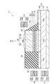
【解決手段】面発光半導体レーザ11は、第1の部分17と該第1の部分上に設けられた第2の部分19とを含む第1のDBR15と、第1のDBR15上に設けられ、活性層23を含む半導体メサ20と、第2のDBR33とを備える。第1の部分17はアンドープの半導体材料からなり、第2の部分19は、III族構成元素としてIn元素及びGa元素並びにV族構成元素としてP元素を含む材料からなる第3のIII−V族化合物半導体層19aと、III族構成元素としてGa元素及びV族構成元素としてAs元素を含む材料からなる第4のIII−V族化合物半導体層19bとを有する。
【選択図】図1
Description
Y. C. Chang et al., Electronics Letters, vol.42, no.22, pp.1281-1283, 2006.
基板13:半絶縁GaAs半導体
第1のDBR15の第1の部分17:アンドープ、Al0.9Ga0.1As/GaAs、32対
第1のDBR15の第2の部分19:Siドープ、In0.5Ga0.5P/GaAs、3対、電子濃度1×1018cm−3
第1のスペーサ層21:Siドープ、GaAs、厚さ40nm
活性層23:In0.2Ga0.8As井戸層、3層
第2のスペーサ層25:Cドープ、GaAs、厚さ40nm
電流狭窄層28:Cドープ、Al0.96Ga0.04As、厚さ15nm
第3のスペーサ層31:Cドープ、GaAs、厚さ20nm
第2のDBR33:Al0.9Ga0.1As/GaAs、22対
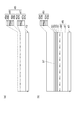
基板73:半絶縁GaAs半導体
第1のDBR75:Siドープ、Al0.9Ga0.1As/GaAs、35対、電子濃度6×1018cm−3
第1のスペーサ層81:Siドープ、GaAs、厚さ40nm
活性層83:In0.2Ga0.8As井戸層、3層
第2のスペーサ層85:Cドープ、GaAs、厚さ40nm
電流狭窄層88:Cドープ、Al0.96Ga0.04As、厚さ15nm
第3のスペーサ層91:Cドープ、GaAs、厚さ20nm
第2のDBR93:Al0.9Ga0.1As/GaAs、22対
半導体レーザA
発振波長:980nm
発振閾値:0.5mA
最大光出力:6mW
微分抵抗:110オーム
比較例B
発振波長:980nm
発振閾値:0.5mA
最大光出力:5.1mW
微分抵抗:240オーム
Claims (7)
- 第1の部分と該第1の部分上に設けられた第2の部分とを含む第1の半導体分布ブラッグリフレクタと、
前記第1の半導体分布ブラッグリフレクタ上に設けられ、活性層を含む半導体メサと、
前記半導体メサ上に設けられた第2の分布ブラッグリフレクタとを備え、
前記第1の半導体分布ブラッグリフレクタの前記第2の部分は、第1の領域と該第1の領域を囲む第2の領域とを有し、
前記半導体メサは、前記第1の領域上に設けられており、
前記第1の半導体分布ブラッグリフレクタの前記第1の部分は、交互に配置された第1のIII−V族化合物半導体層及び第2のIII−V族化合物半導体層を含み、
前記第1の半導体分布ブラッグリフレクタの前記第2の部分は、交互に配置された第3のIII−V族化合物半導体層及び第4のIII−V族化合物半導体層を含み、
前記第1のIII−V族化合物半導体層は、III族構成元素としてAl元素及びGa元素並びにV族構成元素としてAs元素を含むアンドープの半導体材料からなり、
前記第2のIII−V族化合物半導体層は、III族構成元素としてGa元素及びV族構成元素としてAs元素を含むアンドープの半導体材料からなり、
前記第3のIII−V族化合物半導体層は、III族構成元素としてIn元素及びGa元素並びにV族構成元素としてP元素を含む半導体材料からなり、
前記第3のIII−V族化合物半導体層の半導体材料は、n型不純物がドープされた半導体材料またはアンドープの半導体材料であり、
前記第4のIII−V族化合物半導体層は、III族構成元素としてGa元素及びV族構成元素としてAs元素を含む半導体材料からなり、
前記第4のIII−V族化合物半導体層の半導体材料は、n型不純物がドープされた半導体材料である
ことを特徴とする面発光半導体レーザ。 - 前記第1のIII−V族化合物半導体層は、AlGaAs半導体からなり、
前記第2のIII−V族化合物半導体層は、GaAs半導体またはAlGaAs半導体からなることを特徴とする請求項1に記載の面発光半導体レーザ。 - 前記第3のIII−V族化合物半導体層は、InGaP半導体、AlGaInP半導体またはGaInAsP半導体からなることを特徴とする請求項1または請求項2に記載の面発光半導体レーザ。
- 前記第3のIII−V族化合物半導体層は、n型不純物がドープされた半導体材料からなることを特徴とする請求項1〜請求項3のいずれか1項に記載の面発光半導体レーザ。
- 前記第3のIII−V族化合物半導体層は、アンドープの半導体材料からなることを特徴とする請求項1〜請求項3のいずれか1項に記載の面発光半導体レーザ。
- 前記第3のIII−V族化合物半導体層のIII族構成元素におけるIn元素の組成は0.4以上0.5以下であり、
前記第4のIII−V族化合物半導体層は、GaAs半導体からなることを特徴とする請求項1〜請求項5のいずれか1項に記載の面発光半導体レーザ。 - 前記第3のIII−V族化合物半導体層のIII族構成元素におけるIn元素の組成は0.4以上0.6以下であり、
前記第4のIII−V族化合物半導体層は、GaAsP半導体からなることを特徴とする請求項1〜請求項5のいずれか1項に記載の面発光半導体レーザ。
Priority Applications (2)
| Application Number | Priority Date | Filing Date | Title |
|---|---|---|---|
| JP2008184254A JP5169564B2 (ja) | 2008-07-15 | 2008-07-15 | 面発光半導体レーザ |
| US12/437,753 US7852896B2 (en) | 2008-07-15 | 2009-05-08 | Vertical cavity surface emitting laser |
Applications Claiming Priority (1)
| Application Number | Priority Date | Filing Date | Title |
|---|---|---|---|
| JP2008184254A JP5169564B2 (ja) | 2008-07-15 | 2008-07-15 | 面発光半導体レーザ |
Publications (2)
| Publication Number | Publication Date |
|---|---|
| JP2010027697A true JP2010027697A (ja) | 2010-02-04 |
| JP5169564B2 JP5169564B2 (ja) | 2013-03-27 |
Family
ID=41530260
Family Applications (1)
| Application Number | Title | Priority Date | Filing Date |
|---|---|---|---|
| JP2008184254A Expired - Fee Related JP5169564B2 (ja) | 2008-07-15 | 2008-07-15 | 面発光半導体レーザ |
Country Status (2)
| Country | Link |
|---|---|
| US (1) | US7852896B2 (ja) |
| JP (1) | JP5169564B2 (ja) |
Cited By (4)
| Publication number | Priority date | Publication date | Assignee | Title |
|---|---|---|---|---|
| JP2011035115A (ja) * | 2009-07-31 | 2011-02-17 | Canon Inc | 面発光レーザ、面発光レーザアレイ、および光学機器 |
| JP2013093571A (ja) * | 2011-10-04 | 2013-05-16 | Fuji Xerox Co Ltd | 面発光型半導体レーザ、面発光型半導体レーザ装置、光伝送装置および情報処理装置 |
| JP2016213486A (ja) * | 2016-07-14 | 2016-12-15 | 富士ゼロックス株式会社 | 面発光型半導体レーザ、面発光型半導体レーザ装置、光伝送装置および情報処理装置 |
| JP7528798B2 (ja) | 2020-02-25 | 2024-08-06 | 株式会社リコー | 反射鏡、面発光レーザ、面発光レーザアレイ、投影装置、ヘッドアップディスプレイ、移動体、ヘッドマウントディスプレイ、検眼装置及び照明装置 |
Families Citing this family (6)
| Publication number | Priority date | Publication date | Assignee | Title |
|---|---|---|---|---|
| JP6323650B2 (ja) * | 2013-12-20 | 2018-05-16 | セイコーエプソン株式会社 | 面発光レーザーおよび原子発振器 |
| US10530129B2 (en) | 2015-08-10 | 2020-01-07 | Hewlett Packard Enterprise Development Lp | Low impedance VCSELs |
| WO2020005006A1 (ko) * | 2018-06-29 | 2020-01-02 | 엘지이노텍 주식회사 | 표면발광 레이저소자 및 이를 포함하는 발광장치 |
| JP7095498B2 (ja) * | 2018-08-31 | 2022-07-05 | 住友電気工業株式会社 | 垂直共振型面発光レーザ、垂直共振型面発光レーザを作製する方法 |
| KR20230114743A (ko) * | 2020-10-14 | 2023-08-01 | 엑셀리타스 테크놀로지스 코포레이션 | 스트레인 보상 반도체 dbr을 갖는 튜닝 가능 vcsel |
| JP7563186B2 (ja) * | 2021-01-12 | 2024-10-08 | 住友電気工業株式会社 | 垂直共振型面発光レーザ |
Citations (5)
| Publication number | Priority date | Publication date | Assignee | Title |
|---|---|---|---|---|
| JPH04234183A (ja) * | 1990-12-28 | 1992-08-21 | Nec Corp | 面型光半導体素子 |
| JP2001308315A (ja) * | 2000-04-26 | 2001-11-02 | Hitachi Cable Ltd | Iii−v族化合物半導体エピタキシャルウェハ |
| JP2003037335A (ja) * | 2001-07-23 | 2003-02-07 | Furukawa Electric Co Ltd:The | 面発光型半導体レーザ素子 |
| JP2005038995A (ja) * | 2003-07-18 | 2005-02-10 | Ricoh Co Ltd | 積層基体および半導体デバイスおよび光半導体デバイスおよび光伝送システムおよび光電子融合デバイス |
| JP2005158922A (ja) * | 2003-11-25 | 2005-06-16 | Fuji Xerox Co Ltd | 表面発光型半導体レーザ素子およびその製造方法 |
Family Cites Families (2)
| Publication number | Priority date | Publication date | Assignee | Title |
|---|---|---|---|---|
| US7435660B2 (en) * | 1998-12-21 | 2008-10-14 | Finisar Corporation | Migration enhanced epitaxy fabrication of active regions having quantum wells |
| US6927412B2 (en) * | 2002-11-21 | 2005-08-09 | Ricoh Company, Ltd. | Semiconductor light emitter |
-
2008
- 2008-07-15 JP JP2008184254A patent/JP5169564B2/ja not_active Expired - Fee Related
-
2009
- 2009-05-08 US US12/437,753 patent/US7852896B2/en not_active Expired - Fee Related
Patent Citations (5)
| Publication number | Priority date | Publication date | Assignee | Title |
|---|---|---|---|---|
| JPH04234183A (ja) * | 1990-12-28 | 1992-08-21 | Nec Corp | 面型光半導体素子 |
| JP2001308315A (ja) * | 2000-04-26 | 2001-11-02 | Hitachi Cable Ltd | Iii−v族化合物半導体エピタキシャルウェハ |
| JP2003037335A (ja) * | 2001-07-23 | 2003-02-07 | Furukawa Electric Co Ltd:The | 面発光型半導体レーザ素子 |
| JP2005038995A (ja) * | 2003-07-18 | 2005-02-10 | Ricoh Co Ltd | 積層基体および半導体デバイスおよび光半導体デバイスおよび光伝送システムおよび光電子融合デバイス |
| JP2005158922A (ja) * | 2003-11-25 | 2005-06-16 | Fuji Xerox Co Ltd | 表面発光型半導体レーザ素子およびその製造方法 |
Cited By (4)
| Publication number | Priority date | Publication date | Assignee | Title |
|---|---|---|---|---|
| JP2011035115A (ja) * | 2009-07-31 | 2011-02-17 | Canon Inc | 面発光レーザ、面発光レーザアレイ、および光学機器 |
| JP2013093571A (ja) * | 2011-10-04 | 2013-05-16 | Fuji Xerox Co Ltd | 面発光型半導体レーザ、面発光型半導体レーザ装置、光伝送装置および情報処理装置 |
| JP2016213486A (ja) * | 2016-07-14 | 2016-12-15 | 富士ゼロックス株式会社 | 面発光型半導体レーザ、面発光型半導体レーザ装置、光伝送装置および情報処理装置 |
| JP7528798B2 (ja) | 2020-02-25 | 2024-08-06 | 株式会社リコー | 反射鏡、面発光レーザ、面発光レーザアレイ、投影装置、ヘッドアップディスプレイ、移動体、ヘッドマウントディスプレイ、検眼装置及び照明装置 |
Also Published As
| Publication number | Publication date |
|---|---|
| US7852896B2 (en) | 2010-12-14 |
| US20100014551A1 (en) | 2010-01-21 |
| JP5169564B2 (ja) | 2013-03-27 |
Similar Documents
| Publication | Publication Date | Title |
|---|---|---|
| JP5169564B2 (ja) | 面発光半導体レーザ | |
| US7881353B2 (en) | Surface emitting laser element array | |
| US6765238B2 (en) | Material systems for semiconductor tunnel-junction structures | |
| US7123638B2 (en) | Tunnel-junction structure incorporating N-type layer comprising nitrogen and a group VI dopant | |
| JP4663964B2 (ja) | GaAsSb量子井戸層を含む長波長フォトニクスデバイス | |
| US7016392B2 (en) | GaAs-based long-wavelength laser incorporating tunnel junction structure | |
| JP5273516B2 (ja) | トンネル接合発光素子 | |
| JP4172505B2 (ja) | 面発光型半導体素子及び面発光型半導体素子の製造方法 | |
| US8488644B2 (en) | Semiconductor laser element and manufacturing method thereof | |
| US6914925B2 (en) | Vertical cavity surface emitting semiconductor laser device | |
| US20060268954A1 (en) | Light emitting semiconductor device having an electrical confinement barrier near the active region | |
| US20150188289A1 (en) | Surface-emitting laser, surface-emitting laser array, display apparatus including the surface-emitting laser array as a light source, printer head, and printer | |
| JP2009038310A (ja) | 面発光型半導体光デバイス | |
| JP2008235574A (ja) | 面発光半導体レーザ | |
| US20010050935A1 (en) | Surface emitting semiconductor laser device | |
| JP2019033152A (ja) | 垂直共振型面発光レーザ、垂直共振型面発光レーザを作製する方法 | |
| JP2006332623A (ja) | 半導体レーザ装置 | |
| JP2007311632A (ja) | 面発光レーザ素子 | |
| KR102505318B1 (ko) | 동작전압 특성을 개선한 수직 공진 표면 발광 레이저 소자 | |
| JP2021009895A (ja) | 面発光レーザ | |
| WO2021177036A1 (ja) | 面発光レーザ | |
| JP4948451B2 (ja) | 面発光レーザ素子および面発光レーザ素子の製造方法 | |
| JP2010056235A (ja) | 面発光半導体レーザ素子の製造方法 | |
| JP2020017573A (ja) | 垂直共振型面発光レーザ | |
| US12212122B2 (en) | Vertical-cavity surface-emitting laser |
Legal Events
| Date | Code | Title | Description |
|---|---|---|---|
| A621 | Written request for application examination |
Free format text: JAPANESE INTERMEDIATE CODE: A621 Effective date: 20110414 |
|
| A977 | Report on retrieval |
Free format text: JAPANESE INTERMEDIATE CODE: A971007 Effective date: 20120502 |
|
| A131 | Notification of reasons for refusal |
Free format text: JAPANESE INTERMEDIATE CODE: A131 Effective date: 20120515 |
|
| A521 | Request for written amendment filed |
Free format text: JAPANESE INTERMEDIATE CODE: A523 Effective date: 20120713 |
|
| TRDD | Decision of grant or rejection written | ||
| A01 | Written decision to grant a patent or to grant a registration (utility model) |
Free format text: JAPANESE INTERMEDIATE CODE: A01 Effective date: 20121204 |
|
| A61 | First payment of annual fees (during grant procedure) |
Free format text: JAPANESE INTERMEDIATE CODE: A61 Effective date: 20121217 |
|
| R150 | Certificate of patent or registration of utility model |
Ref document number: 5169564 Country of ref document: JP Free format text: JAPANESE INTERMEDIATE CODE: R150 |
|
| R250 | Receipt of annual fees |
Free format text: JAPANESE INTERMEDIATE CODE: R250 |
|
| R250 | Receipt of annual fees |
Free format text: JAPANESE INTERMEDIATE CODE: R250 |
|
| R250 | Receipt of annual fees |
Free format text: JAPANESE INTERMEDIATE CODE: R250 |
|
| R250 | Receipt of annual fees |
Free format text: JAPANESE INTERMEDIATE CODE: R250 |
|
| R250 | Receipt of annual fees |
Free format text: JAPANESE INTERMEDIATE CODE: R250 |
|
| LAPS | Cancellation because of no payment of annual fees |