JP2010027684A - プリント配線基板 - Google Patents
プリント配線基板 Download PDFInfo
- Publication number
- JP2010027684A JP2010027684A JP2008184050A JP2008184050A JP2010027684A JP 2010027684 A JP2010027684 A JP 2010027684A JP 2008184050 A JP2008184050 A JP 2008184050A JP 2008184050 A JP2008184050 A JP 2008184050A JP 2010027684 A JP2010027684 A JP 2010027684A
- Authority
- JP
- Japan
- Prior art keywords
- layer
- printed wiring
- wiring board
- electromagnetic radiation
- power supply
- Prior art date
- Legal status (The legal status is an assumption and is not a legal conclusion. Google has not performed a legal analysis and makes no representation as to the accuracy of the status listed.)
- Granted
Links
- 230000005670 electromagnetic radiation Effects 0.000 claims abstract description 50
- 239000010409 thin film Substances 0.000 claims abstract description 25
- 239000000758 substrate Substances 0.000 claims abstract description 24
- 230000035699 permeability Effects 0.000 claims abstract description 13
- 239000002184 metal Substances 0.000 claims description 12
- 229910052751 metal Inorganic materials 0.000 claims description 12
- 239000010419 fine particle Substances 0.000 claims description 10
- 239000002105 nanoparticle Substances 0.000 claims description 4
- 239000000956 alloy Substances 0.000 claims description 3
- 229910045601 alloy Inorganic materials 0.000 claims description 3
- 229910052782 aluminium Inorganic materials 0.000 claims description 3
- 229910052799 carbon Inorganic materials 0.000 claims description 3
- 229910052802 copper Inorganic materials 0.000 claims description 3
- 229910052742 iron Inorganic materials 0.000 claims description 3
- 229910052749 magnesium Inorganic materials 0.000 claims description 3
- 229910052759 nickel Inorganic materials 0.000 claims description 3
- 229910052710 silicon Inorganic materials 0.000 claims description 3
- 229910052709 silver Inorganic materials 0.000 claims description 3
- 239000004065 semiconductor Substances 0.000 claims description 2
- 238000009413 insulation Methods 0.000 abstract 6
- 230000001747 exhibiting effect Effects 0.000 abstract 1
- 239000010410 layer Substances 0.000 description 144
- 238000010586 diagram Methods 0.000 description 14
- 230000005684 electric field Effects 0.000 description 6
- 230000001629 suppression Effects 0.000 description 6
- 238000005229 chemical vapour deposition Methods 0.000 description 4
- 230000005418 spin wave Effects 0.000 description 4
- 230000000694 effects Effects 0.000 description 3
- 238000000034 method Methods 0.000 description 3
- 230000008054 signal transmission Effects 0.000 description 3
- 238000007740 vapor deposition Methods 0.000 description 3
- 230000005540 biological transmission Effects 0.000 description 2
- 239000004020 conductor Substances 0.000 description 2
- 230000005672 electromagnetic field Effects 0.000 description 2
- 230000003993 interaction Effects 0.000 description 2
- 238000005240 physical vapour deposition Methods 0.000 description 2
- 238000000623 plasma-assisted chemical vapour deposition Methods 0.000 description 2
- 230000001902 propagating effect Effects 0.000 description 2
- 230000005855 radiation Effects 0.000 description 2
- 238000004544 sputter deposition Methods 0.000 description 2
- 238000007751 thermal spraying Methods 0.000 description 2
- 239000000853 adhesive Substances 0.000 description 1
- 230000008901 benefit Effects 0.000 description 1
- 239000011230 binding agent Substances 0.000 description 1
- 239000003990 capacitor Substances 0.000 description 1
- 230000008859 change Effects 0.000 description 1
- 239000011248 coating agent Substances 0.000 description 1
- 238000000576 coating method Methods 0.000 description 1
- 238000004891 communication Methods 0.000 description 1
- 230000008878 coupling Effects 0.000 description 1
- 238000010168 coupling process Methods 0.000 description 1
- 238000005859 coupling reaction Methods 0.000 description 1
- 238000011156 evaluation Methods 0.000 description 1
- 239000000835 fiber Substances 0.000 description 1
- 239000010408 film Substances 0.000 description 1
- 239000003574 free electron Substances 0.000 description 1
- 239000011229 interlayer Substances 0.000 description 1
- 239000012762 magnetic filler Substances 0.000 description 1
- 239000000696 magnetic material Substances 0.000 description 1
- 239000007769 metal material Substances 0.000 description 1
- 239000002245 particle Substances 0.000 description 1
- 229920006267 polyester film Polymers 0.000 description 1
- 239000011347 resin Substances 0.000 description 1
- 229920005989 resin Polymers 0.000 description 1
- 238000004528 spin coating Methods 0.000 description 1
- 239000000126 substance Substances 0.000 description 1
- 230000009466 transformation Effects 0.000 description 1
Images


Classifications
-
- H—ELECTRICITY
- H05—ELECTRIC TECHNIQUES NOT OTHERWISE PROVIDED FOR
- H05K—PRINTED CIRCUITS; CASINGS OR CONSTRUCTIONAL DETAILS OF ELECTRIC APPARATUS; MANUFACTURE OF ASSEMBLAGES OF ELECTRICAL COMPONENTS
- H05K9/00—Screening of apparatus or components against electric or magnetic fields
- H05K9/0073—Shielding materials
- H05K9/0081—Electromagnetic shielding materials, e.g. EMI, RFI shielding
- H05K9/0084—Electromagnetic shielding materials, e.g. EMI, RFI shielding comprising a single continuous metallic layer on an electrically insulating supporting structure, e.g. metal foil, film, plating coating, electro-deposition, vapour-deposition
-
- H—ELECTRICITY
- H05—ELECTRIC TECHNIQUES NOT OTHERWISE PROVIDED FOR
- H05K—PRINTED CIRCUITS; CASINGS OR CONSTRUCTIONAL DETAILS OF ELECTRIC APPARATUS; MANUFACTURE OF ASSEMBLAGES OF ELECTRICAL COMPONENTS
- H05K1/00—Printed circuits
- H05K1/02—Details
- H05K1/0213—Electrical arrangements not otherwise provided for
- H05K1/0216—Reduction of cross-talk, noise or electromagnetic interference
- H05K1/0218—Reduction of cross-talk, noise or electromagnetic interference by printed shielding conductors, ground planes or power plane
-
- H—ELECTRICITY
- H05—ELECTRIC TECHNIQUES NOT OTHERWISE PROVIDED FOR
- H05K—PRINTED CIRCUITS; CASINGS OR CONSTRUCTIONAL DETAILS OF ELECTRIC APPARATUS; MANUFACTURE OF ASSEMBLAGES OF ELECTRICAL COMPONENTS
- H05K1/00—Printed circuits
- H05K1/02—Details
- H05K1/0213—Electrical arrangements not otherwise provided for
- H05K1/0216—Reduction of cross-talk, noise or electromagnetic interference
- H05K1/023—Reduction of cross-talk, noise or electromagnetic interference using auxiliary mounted passive components or auxiliary substances
- H05K1/0234—Resistors or by disposing resistive or lossy substances in or near power planes
-
- H—ELECTRICITY
- H05—ELECTRIC TECHNIQUES NOT OTHERWISE PROVIDED FOR
- H05K—PRINTED CIRCUITS; CASINGS OR CONSTRUCTIONAL DETAILS OF ELECTRIC APPARATUS; MANUFACTURE OF ASSEMBLAGES OF ELECTRICAL COMPONENTS
- H05K1/00—Printed circuits
- H05K1/16—Printed circuits incorporating printed electric components, e.g. printed resistor, capacitor, inductor
- H05K1/167—Printed circuits incorporating printed electric components, e.g. printed resistor, capacitor, inductor incorporating printed resistors
-
- H—ELECTRICITY
- H05—ELECTRIC TECHNIQUES NOT OTHERWISE PROVIDED FOR
- H05K—PRINTED CIRCUITS; CASINGS OR CONSTRUCTIONAL DETAILS OF ELECTRIC APPARATUS; MANUFACTURE OF ASSEMBLAGES OF ELECTRICAL COMPONENTS
- H05K2201/00—Indexing scheme relating to printed circuits covered by H05K1/00
- H05K2201/01—Dielectrics
- H05K2201/0183—Dielectric layers
- H05K2201/0187—Dielectric layers with regions of different dielectrics in the same layer, e.g. in a printed capacitor for locally changing the dielectric properties
-
- H—ELECTRICITY
- H05—ELECTRIC TECHNIQUES NOT OTHERWISE PROVIDED FOR
- H05K—PRINTED CIRCUITS; CASINGS OR CONSTRUCTIONAL DETAILS OF ELECTRIC APPARATUS; MANUFACTURE OF ASSEMBLAGES OF ELECTRICAL COMPONENTS
- H05K2201/00—Indexing scheme relating to printed circuits covered by H05K1/00
- H05K2201/02—Fillers; Particles; Fibers; Reinforcement materials
- H05K2201/0203—Fillers and particles
- H05K2201/0206—Materials
- H05K2201/0215—Metallic fillers
-
- H—ELECTRICITY
- H05—ELECTRIC TECHNIQUES NOT OTHERWISE PROVIDED FOR
- H05K—PRINTED CIRCUITS; CASINGS OR CONSTRUCTIONAL DETAILS OF ELECTRIC APPARATUS; MANUFACTURE OF ASSEMBLAGES OF ELECTRICAL COMPONENTS
- H05K2201/00—Indexing scheme relating to printed circuits covered by H05K1/00
- H05K2201/09—Shape and layout
- H05K2201/09209—Shape and layout details of conductors
- H05K2201/0929—Conductive planes
- H05K2201/09309—Core having two or more power planes; Capacitive laminate of two power planes
-
- H—ELECTRICITY
- H05—ELECTRIC TECHNIQUES NOT OTHERWISE PROVIDED FOR
- H05K—PRINTED CIRCUITS; CASINGS OR CONSTRUCTIONAL DETAILS OF ELECTRIC APPARATUS; MANUFACTURE OF ASSEMBLAGES OF ELECTRICAL COMPONENTS
- H05K3/00—Apparatus or processes for manufacturing printed circuits
- H05K3/40—Forming printed elements for providing electric connections to or between printed circuits
- H05K3/403—Edge contacts; Windows or holes in the substrate having plural connections on the walls thereof
Landscapes
- Physics & Mathematics (AREA)
- Electromagnetism (AREA)
- Engineering & Computer Science (AREA)
- Microelectronics & Electronic Packaging (AREA)
- Shielding Devices Or Components To Electric Or Magnetic Fields (AREA)
- Structure Of Printed Boards (AREA)
- Production Of Multi-Layered Print Wiring Board (AREA)
Abstract
【解決手段】内部に第1の信号配線層1が設けられた絶縁層2には、一方の面に電源層3及び第2の絶縁基板層7が設けられ、他方の面にグランド層4及び第1の絶縁基板層5が設けられている。また、第1の絶縁基板層5には第2の信号配線層6が設けられ、第2の絶縁基板層7には第3の信号配線層8が設けられている。更に、絶縁層2、電源層3及びグランド層4の全側面を被い、電源層3及びグランド層4の表面の一部を被うようにして、薄膜層10を有する電磁放射抑制部材20が設けられている。薄膜層10は、所定の周波数領域を含む周波数領域で、誘電率が負になると共に透磁率が正になる特性を有している。
【選択図】図1
Description
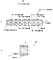
図1は、本発明の第1の実施の形態に係るプリント配線基板を示し、(a)は、全体を示す断面図、(b)は、側部の詳細を示す断面図である。
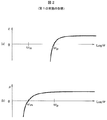
図2は、本発明の第1の実施の形態に係るプリント配線基板における電磁放射抑制部材の周波数特性を示し、(a)は誘電率の周波数特性図、(b)は透磁率の周波数特性図である。図2(a)に示すように、電磁放射抑制部材20の薄膜層10の誘電率εは、プラズモン共鳴が生じる周波数ωp(例えば、100GHz)を境にして、ωpより低い周波数域では誘電率εが負になり、ωpより高い周波数域では誘電率εが正になる。これは、ωpより高い周波数域では、薄膜層10が誘電体として機能することを示している。
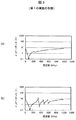
図3(a)は、図1に示したプリント配線基板のインピーダンス特性図、図3(b)は、図1に示したプリント配線基板から電磁放射抑制部材を除去したプリント配線基板のインピーダンス特性図である。図3(b)に示すように、プリント配線基板100に電磁放射抑制部材20を設けないプリント配線基板(従来構成)は、複数の周波数で共振が生じている。これに対し、図3(a)に示す本実施の形態に係るプリント配線基板100は、共振は1つで、VHF帯以上では安定している。このことから、電源層3とグランド層4との間のインピーダンス(電源系インピーダンス)に影響を与えないことがわかる。
図4は、本発明の第1の実施の形態に係るプリント配線基板における等価磁流と電界の生成を説明する図である。電源層3とグランド層4が平行平板共振器を形成して共振周波数にあるとき、電源層3とグランド層4との間の電界Eは、図4に示すように、両端部(図4の左右両端)100a,100bにおいて電位差が最大になる。また、電界Eが発生している両端部100a,100bに電界Eに直交する等価磁流Iemが生じ、この等価磁流Iemに基づいたTEM(transverse Electromagnetic Mode:伝搬方向に電場の成分と磁場の成分がゼロである導波路のモード。)波が空間に電磁波として放射される。この電磁波は、電磁放射抑制部材20の薄膜層10に導電性を誘起し、薄膜層10が導電体となることにより、共振エネルギーが電源層3とグランド層4との間で消費される。この結果、電源層3とグランド層4との間の共振電流が抑制され、同時に、基板端部からの電磁放射が低減する。
図5は、本発明の第1の実施の形態に係るプリント配線基板のS11(入力反射係数)パラメータにおけるリターンロス(反射損失)特性を示し、図5(a)は、図1に示したプリント配線基板のリターンロス特性図、図5(b)は、図1に示したプリント配線基板から電磁放射抑制部材を除去したプリント配線基板のリターンロス特性図である。図5(b)に示すように、プリント配線基板100に電磁放射抑制部材20を設けないプリント配線基板(従来構成)は、複数の共振周波数でリターンロスが発生している。これに対し、図5(a)に示す本実施の形態に係るプリント配線基板100は、共振は発生せず、リターンロスは僅かである。
図6は、EMI(Electromagnetic Interference:電磁妨害)の抑制効果を示し、図6(a)は、図1に示したプリント配線基板の電磁放射特性図、図6(b)は、図1に示したプリント配線基板から電磁放射抑制部材を除去したプリント配線基板の電磁放射特性図である。これらの特性は、10MHzのクロック信号を電源層3とグランド層4との間に印加し、その際の放射ノイズを水平アンテナで受信して観測したものである。
図7は、本発明の第2の実施の形態に係るプリント配線基板を示し、(a)は主要部の断面図、(b)は要部の平面図である。なお、図7(b)においては、電磁放射抑制部材20の図示を省略している。
図8は、本発明の第3の実施の形態に係るプリント配線基板の主要部を示す断面図である。本実施の形態は、第1の実施の形態において、第1,第2の絶縁基板層5,7を絶縁層2と同一サイズにして電源層3及びグランド層4の端部が第1,第2の絶縁基板層5,7のプリプレグで覆われるようにし、更に、第1,第2の絶縁基板層5,7の表面の所定部分が、電磁放射抑制部材20の絶縁シート9及び薄膜層10の両端部で覆われる構成にしたものであり、その他の構成は、第1の実施の形態と同様である。
図9は、本発明の第4の実施の形態に係るプリント配線基板の主要部を示す断面図である。本実施の形態は、第1の実施の形態において、絶縁層2から第1の信号配線層1及び第1,第2の絶縁基板層5,7を除去し、電源層3及びグランド層4に割り込むようにして絶縁層2上に各1つの第2,第3の信号配線層6,8を設けて2層基板としたものであり、その他の構成は、第1の実施の形態と同様である。
なお、本発明は、上記各実施の形態に限定されず、その要旨を変更しない範囲内で種々な変形が可能である。例えば、各実施の形態間の構成要素の組合せは任意に行うことができる。
Claims (4)
- グランド層と、
前記グランド層に対向して設けられた電源層と、
所定の周波数領域で信号を伝送する信号配線層と、
前記グランド層、前記電源層及び前記信号配線層を絶縁する絶縁層と、
前記絶縁層の周縁を被うように設けられ、前記所定の周波数領域を含む周波数領域で誘電率が負であり、かつ、透磁率が正の特性を有する電磁放射抑制部材とを備えたプリント配線基板。 - 前記電磁放射抑制部材は、ナノサイズの金属又は半導体の微粒子を所定の密度で分散させた薄膜層を有する請求項1に記載のプリント配線基板。
- 前記微粒子は、Fe、Al、Ni、Ag,Mg、Cu、Si及びCのうち少なくとも1つからなる合金または共析物である請求項2に記載のプリント配線基板。
- 前記電磁放射抑制部材は、前記薄膜層が被着される絶縁シートを有する請求項2に記載のプリント配線基板。
Priority Applications (2)
| Application Number | Priority Date | Filing Date | Title |
|---|---|---|---|
| JP2008184050A JP5176736B2 (ja) | 2008-07-15 | 2008-07-15 | プリント配線基板 |
| US12/501,931 US8373072B2 (en) | 2008-07-15 | 2009-07-13 | Printed circuit board |
Applications Claiming Priority (1)
| Application Number | Priority Date | Filing Date | Title |
|---|---|---|---|
| JP2008184050A JP5176736B2 (ja) | 2008-07-15 | 2008-07-15 | プリント配線基板 |
Publications (2)
| Publication Number | Publication Date |
|---|---|
| JP2010027684A true JP2010027684A (ja) | 2010-02-04 |
| JP5176736B2 JP5176736B2 (ja) | 2013-04-03 |
Family
ID=41529688
Family Applications (1)
| Application Number | Title | Priority Date | Filing Date |
|---|---|---|---|
| JP2008184050A Active JP5176736B2 (ja) | 2008-07-15 | 2008-07-15 | プリント配線基板 |
Country Status (2)
| Country | Link |
|---|---|
| US (1) | US8373072B2 (ja) |
| JP (1) | JP5176736B2 (ja) |
Cited By (1)
| Publication number | Priority date | Publication date | Assignee | Title |
|---|---|---|---|---|
| JP2015046571A (ja) * | 2013-08-02 | 2015-03-12 | 日本特殊陶業株式会社 | 配線基板およびその製造方法 |
Families Citing this family (7)
| Publication number | Priority date | Publication date | Assignee | Title |
|---|---|---|---|---|
| CN206040982U (zh) | 2013-10-29 | 2017-03-22 | 基马医疗科技有限公司 | 印刷电路板和医疗装置 |
| EP3102100B1 (en) | 2014-02-05 | 2023-08-09 | ZOLL Medical Israel Ltd. | Apparatuses for determining blood pressure |
| WO2016040337A1 (en) | 2014-09-08 | 2016-03-17 | KYMA Medical Technologies, Inc. | Monitoring and diagnostics systems and methods |
| WO2016115175A1 (en) | 2015-01-12 | 2016-07-21 | KYMA Medical Technologies, Inc. | Systems, apparatuses and methods for radio frequency-based attachment sensing |
| US11020002B2 (en) | 2017-08-10 | 2021-06-01 | Zoll Medical Israel Ltd. | Systems, devices and methods for physiological monitoring of patients |
| US11005167B2 (en) * | 2017-11-03 | 2021-05-11 | Antenum Llc | Low profile antenna-conformal one dimensional |
| US10373901B1 (en) * | 2018-09-26 | 2019-08-06 | Taiwan Semiconductor Manufacturing Company Ltd. | Semiconductor structure and manufacturing method thereof |
Citations (5)
| Publication number | Priority date | Publication date | Assignee | Title |
|---|---|---|---|---|
| JPH11177273A (ja) * | 1997-12-08 | 1999-07-02 | Nippon Paint Co Ltd | 電子機器筐体及び不要輻射波低減方法 |
| JP2003218541A (ja) * | 2002-01-24 | 2003-07-31 | Oki Electric Ind Co Ltd | Emi低減構造基板 |
| JP2004327687A (ja) * | 2003-04-24 | 2004-11-18 | Daiwa Fine Chemicals Co Ltd (Laboratory) | 電磁波障害防止用材料 |
| JP2004363347A (ja) * | 2003-06-05 | 2004-12-24 | Oki Electric Ind Co Ltd | 多層プリント基板 |
| US20060237223A1 (en) * | 2005-04-26 | 2006-10-26 | Houfei Chen | Absorbing boundary for a multi-layer circuit board structure |
Family Cites Families (3)
| Publication number | Priority date | Publication date | Assignee | Title |
|---|---|---|---|---|
| JPH0831705B2 (ja) | 1990-08-02 | 1996-03-27 | インターナショナル・ビジネス・マシーンズ・コーポレイション | Emi抑制回路カード |
| JP3036629B2 (ja) | 1996-10-07 | 2000-04-24 | 富士ゼロックス株式会社 | プリント配線基板装置 |
| JP4429961B2 (ja) | 2005-04-13 | 2010-03-10 | 信越ポリマー株式会社 | プリント配線基板およびその製造方法 |
-
2008
- 2008-07-15 JP JP2008184050A patent/JP5176736B2/ja active Active
-
2009
- 2009-07-13 US US12/501,931 patent/US8373072B2/en not_active Expired - Fee Related
Patent Citations (5)
| Publication number | Priority date | Publication date | Assignee | Title |
|---|---|---|---|---|
| JPH11177273A (ja) * | 1997-12-08 | 1999-07-02 | Nippon Paint Co Ltd | 電子機器筐体及び不要輻射波低減方法 |
| JP2003218541A (ja) * | 2002-01-24 | 2003-07-31 | Oki Electric Ind Co Ltd | Emi低減構造基板 |
| JP2004327687A (ja) * | 2003-04-24 | 2004-11-18 | Daiwa Fine Chemicals Co Ltd (Laboratory) | 電磁波障害防止用材料 |
| JP2004363347A (ja) * | 2003-06-05 | 2004-12-24 | Oki Electric Ind Co Ltd | 多層プリント基板 |
| US20060237223A1 (en) * | 2005-04-26 | 2006-10-26 | Houfei Chen | Absorbing boundary for a multi-layer circuit board structure |
Cited By (1)
| Publication number | Priority date | Publication date | Assignee | Title |
|---|---|---|---|---|
| JP2015046571A (ja) * | 2013-08-02 | 2015-03-12 | 日本特殊陶業株式会社 | 配線基板およびその製造方法 |
Also Published As
| Publication number | Publication date |
|---|---|
| US8373072B2 (en) | 2013-02-12 |
| JP5176736B2 (ja) | 2013-04-03 |
| US20100013318A1 (en) | 2010-01-21 |
Similar Documents
| Publication | Publication Date | Title |
|---|---|---|
| JP5176736B2 (ja) | プリント配線基板 | |
| JP2867985B2 (ja) | プリント回路基板 | |
| JP6156610B2 (ja) | 電子機器、およびアンテナ素子 | |
| US6603668B2 (en) | Interlayer structure with multiple insulative layers with different frequency characteristics | |
| JPH09289378A (ja) | プリント配線板及びその製造方法 | |
| WO2002091515A1 (fr) | Composantes de type ligne de transmission | |
| JP6187606B2 (ja) | プリント基板 | |
| JP2011054672A (ja) | 電気磁気素子およびその製造方法 | |
| JP2009283901A (ja) | カバーレイフィルムおよびフレキシブルプリント配線板 | |
| JP6169395B2 (ja) | 共振器 | |
| US10178758B2 (en) | Printed wiring board and method of producing the same | |
| CN103929933A (zh) | 抑制电磁波干扰结构及具有该结构的软性印刷电路板 | |
| CN204333194U (zh) | 高频信号线路 | |
| JPWO2003081973A1 (ja) | 電磁波遮蔽用シート、電磁波遮蔽伝送用ケーブル及び電磁波遮蔽lsi | |
| JP4494714B2 (ja) | プリント配線板 | |
| JP4670853B2 (ja) | 送受信モジュール | |
| JP4968033B2 (ja) | アンテナ装置 | |
| US10111318B2 (en) | Circuit substrate, and noise reduction method for circuit substrate | |
| JP2003218541A (ja) | Emi低減構造基板 | |
| JP4910335B2 (ja) | 印刷配線板及び半導体集積回路装置 | |
| JP2006294769A (ja) | 多層プリント配線基板 | |
| CN204257793U (zh) | 高频信号线路 | |
| JP4540493B2 (ja) | プリント配線基板 | |
| JP2010041555A (ja) | 伝送線路 | |
| JP2001326468A (ja) | 多層プリント配線板及び電子機器 |
Legal Events
| Date | Code | Title | Description |
|---|---|---|---|
| A621 | Written request for application examination |
Free format text: JAPANESE INTERMEDIATE CODE: A621 Effective date: 20110621 |
|
| A977 | Report on retrieval |
Free format text: JAPANESE INTERMEDIATE CODE: A971007 Effective date: 20120614 |
|
| A131 | Notification of reasons for refusal |
Free format text: JAPANESE INTERMEDIATE CODE: A131 Effective date: 20120710 |
|
| RD03 | Notification of appointment of power of attorney |
Free format text: JAPANESE INTERMEDIATE CODE: A7423 Effective date: 20120806 |
|
| A521 | Written amendment |
Free format text: JAPANESE INTERMEDIATE CODE: A523 Effective date: 20120910 |
|
| TRDD | Decision of grant or rejection written | ||
| A01 | Written decision to grant a patent or to grant a registration (utility model) |
Free format text: JAPANESE INTERMEDIATE CODE: A01 Effective date: 20121211 |
|
| A61 | First payment of annual fees (during grant procedure) |
Free format text: JAPANESE INTERMEDIATE CODE: A61 Effective date: 20121224 |
|
| R150 | Certificate of patent or registration of utility model |
Ref document number: 5176736 Country of ref document: JP Free format text: JAPANESE INTERMEDIATE CODE: R150 |
|
| S533 | Written request for registration of change of name |
Free format text: JAPANESE INTERMEDIATE CODE: R313533 |
|
| R350 | Written notification of registration of transfer |
Free format text: JAPANESE INTERMEDIATE CODE: R350 |