JP2010010440A - 成膜方法 - Google Patents
成膜方法 Download PDFInfo
- Publication number
- JP2010010440A JP2010010440A JP2008168597A JP2008168597A JP2010010440A JP 2010010440 A JP2010010440 A JP 2010010440A JP 2008168597 A JP2008168597 A JP 2008168597A JP 2008168597 A JP2008168597 A JP 2008168597A JP 2010010440 A JP2010010440 A JP 2010010440A
- Authority
- JP
- Japan
- Prior art keywords
- substrate
- main surface
- lattice constant
- thin film
- film
- Prior art date
- Legal status (The legal status is an assumption and is not a legal conclusion. Google has not performed a legal analysis and makes no representation as to the accuracy of the status listed.)
- Granted
Links
Images


Classifications
-
- C—CHEMISTRY; METALLURGY
- C23—COATING METALLIC MATERIAL; COATING MATERIAL WITH METALLIC MATERIAL; CHEMICAL SURFACE TREATMENT; DIFFUSION TREATMENT OF METALLIC MATERIAL; COATING BY VACUUM EVAPORATION, BY SPUTTERING, BY ION IMPLANTATION OR BY CHEMICAL VAPOUR DEPOSITION, IN GENERAL; INHIBITING CORROSION OF METALLIC MATERIAL OR INCRUSTATION IN GENERAL
- C23C—COATING METALLIC MATERIAL; COATING MATERIAL WITH METALLIC MATERIAL; SURFACE TREATMENT OF METALLIC MATERIAL BY DIFFUSION INTO THE SURFACE, BY CHEMICAL CONVERSION OR SUBSTITUTION; COATING BY VACUUM EVAPORATION, BY SPUTTERING, BY ION IMPLANTATION OR BY CHEMICAL VAPOUR DEPOSITION, IN GENERAL
- C23C16/00—Chemical coating by decomposition of gaseous compounds, without leaving reaction products of surface material in the coating, i.e. chemical vapour deposition [CVD] processes
- C23C16/22—Chemical coating by decomposition of gaseous compounds, without leaving reaction products of surface material in the coating, i.e. chemical vapour deposition [CVD] processes characterised by the deposition of inorganic material, other than metallic material
- C23C16/30—Deposition of compounds, mixtures or solid solutions, e.g. borides, carbides, nitrides
- C23C16/301—AIII BV compounds, where A is Al, Ga, In or Tl and B is N, P, As, Sb or Bi
- C23C16/303—Nitrides
-
- H—ELECTRICITY
- H10—SEMICONDUCTOR DEVICES; ELECTRIC SOLID-STATE DEVICES NOT OTHERWISE PROVIDED FOR
- H10P—GENERIC PROCESSES OR APPARATUS FOR THE MANUFACTURE OR TREATMENT OF DEVICES COVERED BY CLASS H10
- H10P14/00—Formation of materials, e.g. in the shape of layers or pillars
- H10P14/20—Formation of materials, e.g. in the shape of layers or pillars of semiconductor materials
-
- C—CHEMISTRY; METALLURGY
- C30—CRYSTAL GROWTH
- C30B—SINGLE-CRYSTAL GROWTH; UNIDIRECTIONAL SOLIDIFICATION OF EUTECTIC MATERIAL OR UNIDIRECTIONAL DEMIXING OF EUTECTOID MATERIAL; REFINING BY ZONE-MELTING OF MATERIAL; PRODUCTION OF A HOMOGENEOUS POLYCRYSTALLINE MATERIAL WITH DEFINED STRUCTURE; SINGLE CRYSTALS OR HOMOGENEOUS POLYCRYSTALLINE MATERIAL WITH DEFINED STRUCTURE; AFTER-TREATMENT OF SINGLE CRYSTALS OR A HOMOGENEOUS POLYCRYSTALLINE MATERIAL WITH DEFINED STRUCTURE; APPARATUS THEREFOR
- C30B25/00—Single-crystal growth by chemical reaction of reactive gases, e.g. chemical vapour-deposition growth
- C30B25/02—Epitaxial-layer growth
-
- C—CHEMISTRY; METALLURGY
- C30—CRYSTAL GROWTH
- C30B—SINGLE-CRYSTAL GROWTH; UNIDIRECTIONAL SOLIDIFICATION OF EUTECTIC MATERIAL OR UNIDIRECTIONAL DEMIXING OF EUTECTOID MATERIAL; REFINING BY ZONE-MELTING OF MATERIAL; PRODUCTION OF A HOMOGENEOUS POLYCRYSTALLINE MATERIAL WITH DEFINED STRUCTURE; SINGLE CRYSTALS OR HOMOGENEOUS POLYCRYSTALLINE MATERIAL WITH DEFINED STRUCTURE; AFTER-TREATMENT OF SINGLE CRYSTALS OR A HOMOGENEOUS POLYCRYSTALLINE MATERIAL WITH DEFINED STRUCTURE; APPARATUS THEREFOR
- C30B29/00—Single crystals or homogeneous polycrystalline material with defined structure characterised by the material or by their shape
- C30B29/10—Inorganic compounds or compositions
- C30B29/40—AIIIBV compounds wherein A is B, Al, Ga, In or Tl and B is N, P, As, Sb or Bi
- C30B29/403—AIII-nitrides
-
- H—ELECTRICITY
- H10—SEMICONDUCTOR DEVICES; ELECTRIC SOLID-STATE DEVICES NOT OTHERWISE PROVIDED FOR
- H10P—GENERIC PROCESSES OR APPARATUS FOR THE MANUFACTURE OR TREATMENT OF DEVICES COVERED BY CLASS H10
- H10P14/00—Formation of materials, e.g. in the shape of layers or pillars
- H10P14/20—Formation of materials, e.g. in the shape of layers or pillars of semiconductor materials
- H10P14/29—Formation of materials, e.g. in the shape of layers or pillars of semiconductor materials characterised by the substrates
- H10P14/2901—Materials
- H10P14/2921—Materials being crystalline insulating materials
-
- H—ELECTRICITY
- H10—SEMICONDUCTOR DEVICES; ELECTRIC SOLID-STATE DEVICES NOT OTHERWISE PROVIDED FOR
- H10P—GENERIC PROCESSES OR APPARATUS FOR THE MANUFACTURE OR TREATMENT OF DEVICES COVERED BY CLASS H10
- H10P14/00—Formation of materials, e.g. in the shape of layers or pillars
- H10P14/20—Formation of materials, e.g. in the shape of layers or pillars of semiconductor materials
- H10P14/32—Formation of materials, e.g. in the shape of layers or pillars of semiconductor materials characterised by intermediate layers between substrates and deposited layers
- H10P14/3202—Materials thereof
- H10P14/3214—Materials thereof being Group IIIA-VA semiconductors
- H10P14/3216—Nitrides
-
- H—ELECTRICITY
- H10—SEMICONDUCTOR DEVICES; ELECTRIC SOLID-STATE DEVICES NOT OTHERWISE PROVIDED FOR
- H10P—GENERIC PROCESSES OR APPARATUS FOR THE MANUFACTURE OR TREATMENT OF DEVICES COVERED BY CLASS H10
- H10P14/00—Formation of materials, e.g. in the shape of layers or pillars
- H10P14/20—Formation of materials, e.g. in the shape of layers or pillars of semiconductor materials
- H10P14/34—Deposited materials, e.g. layers
- H10P14/3402—Deposited materials, e.g. layers characterised by the chemical composition
- H10P14/3414—Deposited materials, e.g. layers characterised by the chemical composition being group IIIA-VIA materials
- H10P14/3416—Nitrides
-
- H—ELECTRICITY
- H10—SEMICONDUCTOR DEVICES; ELECTRIC SOLID-STATE DEVICES NOT OTHERWISE PROVIDED FOR
- H10P—GENERIC PROCESSES OR APPARATUS FOR THE MANUFACTURE OR TREATMENT OF DEVICES COVERED BY CLASS H10
- H10P14/00—Formation of materials, e.g. in the shape of layers or pillars
- H10P14/20—Formation of materials, e.g. in the shape of layers or pillars of semiconductor materials
- H10P14/36—Formation of materials, e.g. in the shape of layers or pillars of semiconductor materials characterised by treatments done before the formation of the materials
Landscapes
- Chemical & Material Sciences (AREA)
- Materials Engineering (AREA)
- Organic Chemistry (AREA)
- Metallurgy (AREA)
- Engineering & Computer Science (AREA)
- Crystallography & Structural Chemistry (AREA)
- Chemical Kinetics & Catalysis (AREA)
- General Chemical & Material Sciences (AREA)
- Inorganic Chemistry (AREA)
- Mechanical Engineering (AREA)
- Chemical Vapour Deposition (AREA)
- Crystals, And After-Treatments Of Crystals (AREA)
- Recrystallisation Techniques (AREA)
Abstract
【解決手段】成膜させたい薄膜を構成する材料の格子定数と、薄膜が成膜される基板の一方の主表面を構成する材料の格子定数とに応じて、主表面に沿った方向に対して基板を湾曲させる。そして、基板を湾曲させた状態で、その基板の一方の主表面上に薄膜を成膜させる。
【選択図】図9
Description
赤崎勇編書、「III族窒化物半導体」12章、培風館、1999年、p.230−235 赤崎勇編書、「III族窒化物半導体」8章、培風館、1999年、p.147−165
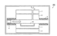
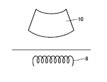
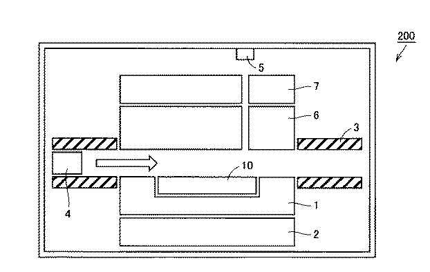
まず、本発明の成膜方法の原理について説明する。図2は、本発明の実施の形態における気相成長による成膜装置の内部の概要を示す概略断面図である。図2に示すように、本発明の実施の形態における気相成長による成膜装置200は基板10をセットするためのサセプタ1の上側に、加熱治具6を介して、サセプタ1の上側の主表面に対向するように配置された第1の加熱部材としてのヒータ7を備えている。また、図2に示すように、サセプタ1の下側にも、第2の加熱部材としてのヒータ2が配置されている。なお、ここで主表面とは、たとえば基板10やサセプタ1などの表面のうち最も面積の大きい、水平方向に沿った方向にセットされている表面をいう。また、ここでいう対向とは、たとえばサセプタ1の上側に、加熱治具6を介して配置されたヒータ7のように、両者間に別の部材が介在する場合も含むこととする。
Claims (10)
- 基板の一方の主表面上に薄膜を成膜させる成膜方法であり、
基板を準備する工程と、
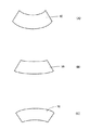
前記主表面に沿った方向に対して前記基板を湾曲させる工程と、
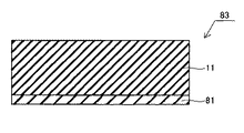
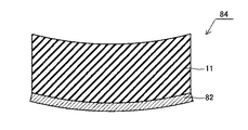
前記基板を湾曲させた状態で、前記基板の一方の主表面上に薄膜を成膜させる工程とを備えている成膜方法。 - 前記基板を湾曲させる工程において前記基板を湾曲させた方向と、前記主表面に沿った方向に対して反対方向に、前記基板を湾曲させる工程と、
前記反対方向に前記基板を湾曲させた状態で、前記基板の一方の主表面上に薄膜を成膜させる工程とをさらに備えている、請求項1に記載の成膜方法。 - 前記基板を湾曲させる工程においては、
成膜させたい前記薄膜を構成する材料の格子定数である第1の格子定数と、前記薄膜が成膜される前記基板の一方の主表面を構成する材料の格子定数である第2の格子定数と、に応じて、前記主表面に沿った方向に対して前記基板を湾曲させる、請求項1または2に記載の成膜方法。 - 前記基板を湾曲させる工程においては、
前記第1の格子定数が、前記第2の格子定数よりも大きければ、前記基板を、前記基板を湾曲させる工程を行なう前の形状よりも、前記一方の主表面側に凸向きの方向に湾曲させ、前記第1の格子定数が、前記第2の格子定数よりも小さければ、前記基板を、前記基板を湾曲させる工程を行なう前の形状よりも、前記一方の主表面側に凹向きの方向に湾曲させる、請求項1〜3のいずれか1項に記載の成膜方法。 - 前記基板を湾曲させる工程においては、
前記第1の格子定数が、前記第2の格子定数よりも大きければ、前記基板を、前記一方の主表面側に凸形状となるように湾曲させ、前記第1の格子定数が、前記第2の格子定数よりも小さければ、前記基板を、前記一方の主表面側に凹形状となるように湾曲させる、請求項1〜3のいずれか1項に記載の成膜方法。 - 前記基板を湾曲させる工程においては、前記基板の一方の主表面に対向するように配置された第1の加熱部材と、前記一方の主表面と反対側に位置する前記基板の他方の主表面に対向するように配置された第2の加熱部材との加熱温度を独立に制御して、前記基板を湾曲させる、請求項1〜5のいずれか1項に記載の成膜方法。
- 前記基板を準備する工程においては、互いに熱膨張係数の異なる材料からなる複数の層が積層した基板を準備する、請求項1〜6のいずれか1項に記載の成膜方法。
- 前記薄膜を成膜させる工程においては、加熱させた前記基板の一方の主表面上に、成膜させたい薄膜を構成する成分の原料ガスを供給する、請求項1〜7のいずれか1項に記載の成膜方法。
- 前記原料ガスは有機金属化合物の蒸気を含む、請求項8に記載の成膜方法。
- 前記原料ガスはIII族元素の化合物の蒸気を含む、請求項8または9に記載の成膜方法。
Priority Applications (7)
| Application Number | Priority Date | Filing Date | Title |
|---|---|---|---|
| JP2008168597A JP5343419B2 (ja) | 2008-06-27 | 2008-06-27 | 成膜方法 |
| CN2009801245094A CN102077319B (zh) | 2008-06-27 | 2009-06-25 | 膜淀积方法 |
| US13/000,835 US8404571B2 (en) | 2008-06-27 | 2009-06-25 | Film deposition method |
| KR1020117000250A KR20110022041A (ko) | 2008-06-27 | 2009-06-25 | 성막 방법 |
| PCT/JP2009/061633 WO2009157514A1 (ja) | 2008-06-27 | 2009-06-25 | 成膜方法 |
| EP09770224.5A EP2312616B1 (en) | 2008-06-27 | 2009-06-25 | Film deposition method |
| TW098121674A TW201009898A (en) | 2008-06-27 | 2009-06-26 | Film deposition method |
Applications Claiming Priority (1)
| Application Number | Priority Date | Filing Date | Title |
|---|---|---|---|
| JP2008168597A JP5343419B2 (ja) | 2008-06-27 | 2008-06-27 | 成膜方法 |
Publications (2)
| Publication Number | Publication Date |
|---|---|
| JP2010010440A true JP2010010440A (ja) | 2010-01-14 |
| JP5343419B2 JP5343419B2 (ja) | 2013-11-13 |
Family
ID=41444577
Family Applications (1)
| Application Number | Title | Priority Date | Filing Date |
|---|---|---|---|
| JP2008168597A Expired - Fee Related JP5343419B2 (ja) | 2008-06-27 | 2008-06-27 | 成膜方法 |
Country Status (7)
| Country | Link |
|---|---|
| US (1) | US8404571B2 (ja) |
| EP (1) | EP2312616B1 (ja) |
| JP (1) | JP5343419B2 (ja) |
| KR (1) | KR20110022041A (ja) |
| CN (1) | CN102077319B (ja) |
| TW (1) | TW201009898A (ja) |
| WO (1) | WO2009157514A1 (ja) |
Cited By (5)
| Publication number | Priority date | Publication date | Assignee | Title |
|---|---|---|---|---|
| JP2013131646A (ja) * | 2011-12-21 | 2013-07-04 | Sharp Corp | 結晶成長装置及び結晶成長方法 |
| JP2016160164A (ja) * | 2015-03-05 | 2016-09-05 | 日本電信電話株式会社 | 結晶成長方法 |
| US9910319B2 (en) | 2014-09-03 | 2018-03-06 | Samsung Display Co., Ltd. | Method of manufacturing curved liquid crystal display panel and apparatus for manufacturing curved liquid crystal display panel |
| JP2018117005A (ja) * | 2017-01-17 | 2018-07-26 | 国立大学法人名古屋大学 | 気相成長装置 |
| JP2022528476A (ja) * | 2019-04-12 | 2022-06-10 | エピルバック エービー | 成長中にウェハの平面性を提供する装置および方法 |
Families Citing this family (2)
| Publication number | Priority date | Publication date | Assignee | Title |
|---|---|---|---|---|
| TWI463194B (zh) * | 2012-03-30 | 2014-12-01 | Sintai Optical Shenzhen Co Ltd | Infrared cutoff filter structure |
| WO2020027993A1 (en) | 2018-08-03 | 2020-02-06 | Applied Materials, Inc. | Multizone lamp control and individual lamp control in a lamphead |
Citations (5)
| Publication number | Priority date | Publication date | Assignee | Title |
|---|---|---|---|---|
| JPH05251427A (ja) * | 1992-03-05 | 1993-09-28 | Nippon Steel Corp | 薄膜の形成方法 |
| JP2003197535A (ja) * | 2001-12-21 | 2003-07-11 | Sumitomo Mitsubishi Silicon Corp | 気相成長装置および気相成長装置の温度検出方法ならびに温度制御方法 |
| JP2004349402A (ja) * | 2003-05-21 | 2004-12-09 | Sharp Corp | 半導体の結晶成長方法、結晶成長装置及びそれらを用いて形成された半導体基板 |
| JP2007214344A (ja) * | 2006-02-09 | 2007-08-23 | Sanyo Electric Co Ltd | 化合物半導体膜の形成方法 |
| JP2007273814A (ja) * | 2006-03-31 | 2007-10-18 | Furukawa Electric Co Ltd:The | シリコン基板及びその製造方法 |
Family Cites Families (10)
| Publication number | Priority date | Publication date | Assignee | Title |
|---|---|---|---|---|
| US3808674A (en) * | 1972-08-10 | 1974-05-07 | Westinghouse Electric Corp | Epitaxial growth of thermically expandable films and particularly anisotropic ferro-electric films |
| US4830984A (en) * | 1987-08-19 | 1989-05-16 | Texas Instruments Incorporated | Method for heteroepitaxial growth using tensioning layer on rear substrate surface |
| DE68923890T2 (de) * | 1988-02-25 | 1996-02-22 | Japan Res Dev Corp | Strahlenoptische Elemente mit Graphit-Schichten. |
| US5044943A (en) * | 1990-08-16 | 1991-09-03 | Applied Materials, Inc. | Spoked susceptor support for enhanced thermal uniformity of susceptor in semiconductor wafer processing apparatus |
| JP3274190B2 (ja) * | 1992-09-26 | 2002-04-15 | 株式会社東芝 | 半導体エピタキシャル基板の製造方法 |
| DE69503285T2 (de) * | 1994-04-07 | 1998-11-05 | Sumitomo Electric Industries | Diamantwafer und Verfahren zur Herstellung eines Diamantwafers |
| US7198671B2 (en) * | 2001-07-11 | 2007-04-03 | Matsushita Electric Industrial Co., Ltd. | Layered substrates for epitaxial processing, and device |
| KR100698014B1 (ko) * | 2004-11-04 | 2007-03-23 | 한국전자통신연구원 | 발광 소자용 실리콘 질화막, 이를 이용한 발광 소자 및발광 소자용 실리콘 질화막의 제조방법 |
| US7262112B2 (en) * | 2005-06-27 | 2007-08-28 | The Regents Of The University Of California | Method for producing dislocation-free strained crystalline films |
| WO2009155122A2 (en) * | 2008-05-30 | 2009-12-23 | Alta Devices, Inc. | Epitaxial lift off stacks and methods |
-
2008
- 2008-06-27 JP JP2008168597A patent/JP5343419B2/ja not_active Expired - Fee Related
-
2009
- 2009-06-25 EP EP09770224.5A patent/EP2312616B1/en not_active Not-in-force
- 2009-06-25 CN CN2009801245094A patent/CN102077319B/zh not_active Expired - Fee Related
- 2009-06-25 WO PCT/JP2009/061633 patent/WO2009157514A1/ja not_active Ceased
- 2009-06-25 US US13/000,835 patent/US8404571B2/en not_active Expired - Fee Related
- 2009-06-25 KR KR1020117000250A patent/KR20110022041A/ko not_active Withdrawn
- 2009-06-26 TW TW098121674A patent/TW201009898A/zh unknown
Patent Citations (5)
| Publication number | Priority date | Publication date | Assignee | Title |
|---|---|---|---|---|
| JPH05251427A (ja) * | 1992-03-05 | 1993-09-28 | Nippon Steel Corp | 薄膜の形成方法 |
| JP2003197535A (ja) * | 2001-12-21 | 2003-07-11 | Sumitomo Mitsubishi Silicon Corp | 気相成長装置および気相成長装置の温度検出方法ならびに温度制御方法 |
| JP2004349402A (ja) * | 2003-05-21 | 2004-12-09 | Sharp Corp | 半導体の結晶成長方法、結晶成長装置及びそれらを用いて形成された半導体基板 |
| JP2007214344A (ja) * | 2006-02-09 | 2007-08-23 | Sanyo Electric Co Ltd | 化合物半導体膜の形成方法 |
| JP2007273814A (ja) * | 2006-03-31 | 2007-10-18 | Furukawa Electric Co Ltd:The | シリコン基板及びその製造方法 |
Cited By (7)
| Publication number | Priority date | Publication date | Assignee | Title |
|---|---|---|---|---|
| JP2013131646A (ja) * | 2011-12-21 | 2013-07-04 | Sharp Corp | 結晶成長装置及び結晶成長方法 |
| US9910319B2 (en) | 2014-09-03 | 2018-03-06 | Samsung Display Co., Ltd. | Method of manufacturing curved liquid crystal display panel and apparatus for manufacturing curved liquid crystal display panel |
| JP2016160164A (ja) * | 2015-03-05 | 2016-09-05 | 日本電信電話株式会社 | 結晶成長方法 |
| JP2018117005A (ja) * | 2017-01-17 | 2018-07-26 | 国立大学法人名古屋大学 | 気相成長装置 |
| WO2018135422A1 (ja) * | 2017-01-17 | 2018-07-26 | 国立大学法人名古屋大学 | 気相成長装置 |
| JP2022528476A (ja) * | 2019-04-12 | 2022-06-10 | エピルバック エービー | 成長中にウェハの平面性を提供する装置および方法 |
| JP7581608B2 (ja) | 2019-04-12 | 2024-11-13 | ヴェエコ エスアイシー シーブイディ システムズ エービー | 成長中にウェハの平面性を提供する装置および方法 |
Also Published As
| Publication number | Publication date |
|---|---|
| CN102077319A (zh) | 2011-05-25 |
| EP2312616A1 (en) | 2011-04-20 |
| EP2312616B1 (en) | 2013-08-07 |
| US8404571B2 (en) | 2013-03-26 |
| WO2009157514A1 (ja) | 2009-12-30 |
| EP2312616A4 (en) | 2011-09-07 |
| KR20110022041A (ko) | 2011-03-04 |
| JP5343419B2 (ja) | 2013-11-13 |
| US20110097880A1 (en) | 2011-04-28 |
| CN102077319B (zh) | 2012-11-28 |
| TW201009898A (en) | 2010-03-01 |
Similar Documents
| Publication | Publication Date | Title |
|---|---|---|
| JP5343419B2 (ja) | 成膜方法 | |
| JP5274785B2 (ja) | AlGaN結晶層の形成方法 | |
| JP5697246B2 (ja) | エピタキシャル成長用サセプタ、これを用いたエピタキシャル成長装置およびこれを用いたエピタキシャル成長方法 | |
| JP5244487B2 (ja) | 窒化ガリウム成長用基板及び窒化ガリウム基板の製造方法 | |
| US20060226414A1 (en) | Group III-V nitride-based semiconductor substrate and method of making same | |
| JP4769905B2 (ja) | p型AlGaN層の製造方法およびIII族窒化物半導体発光素子 | |
| KR101672213B1 (ko) | 반도체장치의 제조방법 | |
| JP4907476B2 (ja) | 窒化物半導体単結晶 | |
| JP4467615B2 (ja) | 窒化物半導体結晶の成長方法、成長装置、および、プログラム | |
| JP2005536883A (ja) | AlGaN単層またはAlGaN多層構造のMBE成長 | |
| JP2006278477A (ja) | 半導体成長用基板、エピタキシャル基板とそれを用いた半導体装置、および、エピタキシャル基板の製造方法 | |
| US20030070610A1 (en) | Method and device for producing group III-N, group III-V-N and metal-nitrogen component structures on Si substrates | |
| JP2009295685A (ja) | 成膜装置 | |
| JP2014003056A (ja) | 半導体積層構造およびこれを用いた半導体素子 | |
| JP2005353680A (ja) | エピタキシャル基板、半導体積層構造、およびエピタキシャル基板の製造方法 | |
| KR20090077471A (ko) | 질화갈륨 성장용 서셉터 및 질화갈륨 성장 방법 | |
| JP5015480B2 (ja) | 半導体単結晶基板の製造方法 | |
| JP2010123818A (ja) | 窒化物半導体多層構造体及びその製造方法 | |
| JP4578282B2 (ja) | アルミニウム系iii族窒化物結晶の製造方法 | |
| JP5898347B2 (ja) | 発光素子の製造方法 | |
| JP2012101977A (ja) | 窒化物半導体基板の製造方法及び窒化物半導体自立基板の製造方法 | |
| JP2011151422A (ja) | p型AlGaN層およびIII族窒化物半導体発光素子 | |
| JP2008044842A (ja) | Iii−v族窒化物系半導体基板 | |
| JP2004111865A (ja) | 半導体基板及びその製造方法 | |
| JP2007227494A (ja) | 発光素子形成用の積層構造体、発光素子、および発光素子の製造方法 |
Legal Events
| Date | Code | Title | Description |
|---|---|---|---|
| A621 | Written request for application examination |
Free format text: JAPANESE INTERMEDIATE CODE: A621 Effective date: 20101214 |
|
| A131 | Notification of reasons for refusal |
Free format text: JAPANESE INTERMEDIATE CODE: A131 Effective date: 20130416 |
|
| A521 | Request for written amendment filed |
Free format text: JAPANESE INTERMEDIATE CODE: A523 Effective date: 20130605 |
|
| TRDD | Decision of grant or rejection written | ||
| A01 | Written decision to grant a patent or to grant a registration (utility model) |
Free format text: JAPANESE INTERMEDIATE CODE: A01 Effective date: 20130716 |
|
| A61 | First payment of annual fees (during grant procedure) |
Free format text: JAPANESE INTERMEDIATE CODE: A61 Effective date: 20130729 |
|
| R150 | Certificate of patent or registration of utility model |
Free format text: JAPANESE INTERMEDIATE CODE: R150 |
|
| LAPS | Cancellation because of no payment of annual fees |