JP2010009002A - 最小面積の液晶表示素子 - Google Patents
最小面積の液晶表示素子 Download PDFInfo
- Publication number
- JP2010009002A JP2010009002A JP2008333285A JP2008333285A JP2010009002A JP 2010009002 A JP2010009002 A JP 2010009002A JP 2008333285 A JP2008333285 A JP 2008333285A JP 2008333285 A JP2008333285 A JP 2008333285A JP 2010009002 A JP2010009002 A JP 2010009002A
- Authority
- JP
- Japan
- Prior art keywords
- region
- liquid crystal
- substrate
- crystal display
- area
- Prior art date
- Legal status (The legal status is an assumption and is not a legal conclusion. Google has not performed a legal analysis and makes no representation as to the accuracy of the status listed.)
- Granted
Links
Images


Classifications
-
- G—PHYSICS
- G02—OPTICS
- G02F—OPTICAL DEVICES OR ARRANGEMENTS FOR THE CONTROL OF LIGHT BY MODIFICATION OF THE OPTICAL PROPERTIES OF THE MEDIA OF THE ELEMENTS INVOLVED THEREIN; NON-LINEAR OPTICS; FREQUENCY-CHANGING OF LIGHT; OPTICAL LOGIC ELEMENTS; OPTICAL ANALOGUE/DIGITAL CONVERTERS
- G02F1/00—Devices or arrangements for the control of the intensity, colour, phase, polarisation or direction of light arriving from an independent light source, e.g. switching, gating or modulating; Non-linear optics
- G02F1/01—Devices or arrangements for the control of the intensity, colour, phase, polarisation or direction of light arriving from an independent light source, e.g. switching, gating or modulating; Non-linear optics for the control of the intensity, phase, polarisation or colour
- G02F1/13—Devices or arrangements for the control of the intensity, colour, phase, polarisation or direction of light arriving from an independent light source, e.g. switching, gating or modulating; Non-linear optics for the control of the intensity, phase, polarisation or colour based on liquid crystals, e.g. single liquid crystal display cells
- G02F1/133—Constructional arrangements; Operation of liquid crystal cells; Circuit arrangements
- G02F1/1333—Constructional arrangements; Manufacturing methods
- G02F1/1345—Conductors connecting electrodes to cell terminals
-
- G—PHYSICS
- G02—OPTICS
- G02F—OPTICAL DEVICES OR ARRANGEMENTS FOR THE CONTROL OF LIGHT BY MODIFICATION OF THE OPTICAL PROPERTIES OF THE MEDIA OF THE ELEMENTS INVOLVED THEREIN; NON-LINEAR OPTICS; FREQUENCY-CHANGING OF LIGHT; OPTICAL LOGIC ELEMENTS; OPTICAL ANALOGUE/DIGITAL CONVERTERS
- G02F1/00—Devices or arrangements for the control of the intensity, colour, phase, polarisation or direction of light arriving from an independent light source, e.g. switching, gating or modulating; Non-linear optics
- G02F1/01—Devices or arrangements for the control of the intensity, colour, phase, polarisation or direction of light arriving from an independent light source, e.g. switching, gating or modulating; Non-linear optics for the control of the intensity, phase, polarisation or colour
- G02F1/13—Devices or arrangements for the control of the intensity, colour, phase, polarisation or direction of light arriving from an independent light source, e.g. switching, gating or modulating; Non-linear optics for the control of the intensity, phase, polarisation or colour based on liquid crystals, e.g. single liquid crystal display cells
- G02F1/133—Constructional arrangements; Operation of liquid crystal cells; Circuit arrangements
- G02F1/1333—Constructional arrangements; Manufacturing methods
- G02F1/133388—Constructional arrangements; Manufacturing methods with constructional differences between the display region and the peripheral region
-
- H—ELECTRICITY
- H10—SEMICONDUCTOR DEVICES; ELECTRIC SOLID-STATE DEVICES NOT OTHERWISE PROVIDED FOR
- H10D—INORGANIC ELECTRIC SEMICONDUCTOR DEVICES
- H10D86/00—Integrated devices formed in or on insulating or conducting substrates, e.g. formed in silicon-on-insulator [SOI] substrates or on stainless steel or glass substrates
- H10D86/40—Integrated devices formed in or on insulating or conducting substrates, e.g. formed in silicon-on-insulator [SOI] substrates or on stainless steel or glass substrates characterised by multiple TFTs
- H10D86/60—Integrated devices formed in or on insulating or conducting substrates, e.g. formed in silicon-on-insulator [SOI] substrates or on stainless steel or glass substrates characterised by multiple TFTs wherein the TFTs are in active matrices
Landscapes
- Physics & Mathematics (AREA)
- Nonlinear Science (AREA)
- Mathematical Physics (AREA)
- Chemical & Material Sciences (AREA)
- Crystallography & Structural Chemistry (AREA)
- General Physics & Mathematics (AREA)
- Optics & Photonics (AREA)
- Liquid Crystal (AREA)
- Devices For Indicating Variable Information By Combining Individual Elements (AREA)
Abstract
【解決手段】前記液晶表示素子は、複数のゲートライン及びデータラインにより定義され、複数の薄膜トランジスタを備えて画像を実現する表示領域と、反射層が備えられて入力される光を反射する反射モードで色を実現する第1領域、並びに入力される光を遮断して駆動回路パターン及び駆動回路を備える第2領域からなり、前記表示領域の外縁部に形成されて設定された輝度の色を実現する周縁領域と、前記周縁領域の外縁部に形成されて駆動回路を備える外郭領域とからなる。
【選択図】図3
Description
このような必要性から、最近は、ゲート駆動回路基板及びデータ駆動回路基板を1つに統合して液晶パネルの一面に実装するGIP(Gate In Panel)構造の液晶表示素子が提案されている。
図4に示すように、従来の液晶表示素子10は、実際に画像が実現される表示領域20と、表示領域20の外縁部に形成され、設定された輝度の色を表示して表示領域20の額縁効果を発揮する周縁領域30と、周縁領域30の外縁部に設置され、ゲート駆動回路及びデータ駆動回路などの駆動回路が形成されて表示領域20内に信号を印加する外郭領域40とからなる。
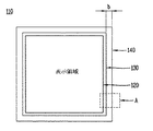
図1は、本発明による液晶表示素子の構造を示す平面図である。図1に示すように、本発明による液晶表示素子110は、実際に画像が実現される表示領域120と、表示領域120の外縁部に形成され、設定された輝度の色を画面の周縁部に表示して額縁効果を発揮する周縁領域130と、周縁領域130の外縁部に設置され、ゲート駆動回路及びデータ駆動回路などの駆動回路が形成されて表示領域120内に信号を印加する外郭領域140とからなる。
図3に示すように、本発明による液晶表示素子は、透明なガラスなどで形成された第1基板210及び第2基板250と、第1基板210と第2基板250との間に形成された液晶層270とからなる。ここで、前記液晶表示素子は、表示領域と周縁領域及び外郭領域とからなり、前記周縁領域は、第1領域及び第2領域とからなる。
前記周縁領域は、多様な形態の動画像が実現される領域でなく、設定された輝度の色を画面の周縁部に実現することにより、表示領域の表示品質を向上させる役割を果たす。実際に、周縁領域に実現される色の輝度は、前記表示領域に実現される画像の品質を向上させるために、前記表示領域の輝度より非常に低く実現される必要があるので、高くなくてもよい。従って、電力消費が多い透過モードではなく、反射モードで前記周縁領域の色を実現しても所望の輝度が得られる。
前述したように、前記周縁領域は、設定された輝度の色を実現するが、実際に画像が実現される画像表示領域である。しかしながら、前記周縁領域に実現される画像は、前記表示領域と前記外郭領域とを区分し、前記表示領域に表示される画像をより高品質に表示するためのものである。よって、前記周縁領域に表示される画像又は色の輝度が前記表示領域に表示される画像又は色の輝度より高い場合、前記周縁領域の画像が表示領域に実現される実際の画像の鑑賞の妨げとなる。従って、前記周縁領域に実現される画像は、低い輝度を有する必要があるため、前記周縁領域の第2領域にブラックマトリクス252を形成する。前記第2領域にブラックマトリクス252を形成することにより、外部から前記第2領域に入射する光の一部を遮断することができ、前記第1領域に入射して反射層234で反射する光のみが液晶層270を透過するので、輝度を低く形成することができる。
ここで、前記薄膜トランジスタは、非晶質半導体で形成することもでき、結晶質半導体で形成することもできるが、ゲート駆動回路262の薄膜トランジスタは非晶質半導体で形成し、データ駆動回路264の薄膜トランジスタは結晶質半導体で形成することが好ましい。
Claims (10)
- 複数のゲートライン及びデータラインにより定義される複数の画素、及び複数の薄膜トランジスタを備えて画像を実現する表示領域と、
反射層が備えられて入力される光を反射する反射モードで色を実現する第1領域、並びに入力される光を遮断して駆動回路パターン及び駆動回路を備える第2領域からなり、前記表示領域の外縁部に形成されて設定された輝度の色を実現する周縁領域と、
前記周縁領域の外縁部に形成されて駆動回路を備える外郭領域と
とから構成される液晶表示素子。 - 前記表示領域は、
第1基板及び第2基板と、
第1基板に形成されたゲート電極、前記ゲート電極上に形成されたゲート絶縁層、前記ゲート絶縁層上に形成された半導体層、前記半導体層上に形成されたソース電極及びドレイン電極からなる薄膜トランジスタと、
前記薄膜トランジスタが形成された第1基板の全体に形成された第1保護膜と、
前記第1保護膜に形成されて薄膜トランジスタのドレイン電極と電気的に接続される画素電極と、
第2基板に形成されたブラックマトリクス及びカラーフィルタ層と、
前記第1基板と第2基板間に形成された液晶層とからなることを特徴とする請求項1に記載の液晶表示素子。 - 前記第1保護膜は、無機物質又は有機物質で形成されることを特徴とする請求項2に記載の液晶表示素子。
- 前記周縁領域は、
第1基板の第2領域に形成された駆動回路パターンと、
第1基板の第1領域及び第2領域に形成された第1保護膜と、
第1領域の第1保護膜に形成された第2保護膜と、
前記第2保護膜に形成された反射層と、
前記反射層に形成された画素電極と、
第2領域の第1保護膜に形成されて前記駆動回路パターンと電気的に接続される接続パターンと、
第2基板に形成されたカラーフィルタ及び前記第2基板の第2領域に形成されたブラックマトリクスと、
前記第1基板と第2基板間に形成された液晶層とからなることを特徴とする請求項1に記載の液晶表示素子。 - 前記画素電極及び前記接続パターンは、同時に形成されることを特徴とする請求項4に記載の液晶表示素子。
- 前記駆動回路パターンは、ゲートパターン及びデータパターンの少なくとも1つを含むことを特徴とする請求項4に記載の液晶表示素子。
- 前記周縁領域は、前記第2領域に形成された駆動回路をさらに含むことを特徴とする請求項4に記載の液晶表示素子。
- 前記第2保護膜は、有機物質で形成されることを特徴とする請求項3に記載の液晶表示素子。
- 前記外郭領域は、第1基板に形成された駆動回路を含むことを特徴とする請求項1に記載の液晶表示素子。
- 前記駆動回路は、ゲート駆動回路及びデータ駆動回路の少なくとも1つを含むことを特徴とする請求項9に記載の液晶表示素子。
Applications Claiming Priority (2)
| Application Number | Priority Date | Filing Date | Title |
|---|---|---|---|
| KR1020080060427A KR101386577B1 (ko) | 2008-06-25 | 2008-06-25 | 면적이 최소화된 액정표시소자 |
| KR10-2008-0060427 | 2008-06-25 |
Publications (2)
| Publication Number | Publication Date |
|---|---|
| JP2010009002A true JP2010009002A (ja) | 2010-01-14 |
| JP5627179B2 JP5627179B2 (ja) | 2014-11-19 |
Family
ID=41446966
Family Applications (1)
| Application Number | Title | Priority Date | Filing Date |
|---|---|---|---|
| JP2008333285A Active JP5627179B2 (ja) | 2008-06-25 | 2008-12-26 | 最小面積の液晶表示素子 |
Country Status (5)
| Country | Link |
|---|---|
| US (1) | US7973888B2 (ja) |
| JP (1) | JP5627179B2 (ja) |
| KR (1) | KR101386577B1 (ja) |
| CN (1) | CN101614892B (ja) |
| TW (1) | TWI414850B (ja) |
Cited By (1)
| Publication number | Priority date | Publication date | Assignee | Title |
|---|---|---|---|---|
| JP2022166948A (ja) * | 2021-04-22 | 2022-11-04 | セイコーエプソン株式会社 | 電気光学装置および電子機器 |
Families Citing this family (12)
| Publication number | Priority date | Publication date | Assignee | Title |
|---|---|---|---|---|
| TWI491303B (zh) * | 2009-06-29 | 2015-07-01 | 群創光電股份有限公司 | 影像顯示系統 |
| KR101609033B1 (ko) * | 2010-08-07 | 2016-04-04 | 샤프 가부시키가이샤 | 박막 트랜지스터 기판 및 이를 구비한 액정표시장치 |
| TWI450144B (zh) * | 2011-04-29 | 2014-08-21 | Wintek Corp | 觸控顯示面板 |
| CN106873231B (zh) * | 2011-07-11 | 2020-10-16 | 大日本印刷株式会社 | 彩色滤光片形成基板及其制作方法以及显示装置 |
| TWI476480B (zh) * | 2011-12-26 | 2015-03-11 | Innolux Corp | 顯示面板及其製造方法與應用之觸控顯示系統 |
| KR101879831B1 (ko) * | 2012-03-21 | 2018-07-20 | 삼성디스플레이 주식회사 | 플렉시블 표시 장치, 유기 발광 표시 장치 및 플렉시블 표시 장치용 원장 기판 |
| KR101969319B1 (ko) * | 2012-06-29 | 2019-04-16 | 엘지디스플레이 주식회사 | 베젤 경계가 투명한 표시소자 |
| KR101695296B1 (ko) * | 2012-12-27 | 2017-01-13 | 엘지디스플레이 주식회사 | 박막트랜지스터 어레이 기판 및 그의 제조방법 |
| CN103943637B (zh) * | 2014-04-10 | 2016-08-31 | 京东方科技集团股份有限公司 | 一种阵列基板、其制作方法及显示装置 |
| KR102343277B1 (ko) * | 2015-03-26 | 2021-12-24 | 삼성디스플레이 주식회사 | 반사층을 포함하는 표시 장치 |
| KR102426498B1 (ko) * | 2015-12-24 | 2022-07-27 | 엘지디스플레이 주식회사 | 터치 표시장치용 어레이기판 및 그 제조방법 |
| KR102494467B1 (ko) * | 2017-12-29 | 2023-01-31 | 엘지디스플레이 주식회사 | 표시 장치 |
Citations (7)
| Publication number | Priority date | Publication date | Assignee | Title |
|---|---|---|---|---|
| JP2001222017A (ja) * | 1999-05-24 | 2001-08-17 | Fujitsu Ltd | 液晶表示装置及びその製造方法 |
| JP2005165051A (ja) * | 2003-12-03 | 2005-06-23 | Seiko Epson Corp | 電気光学装置及び電子機器 |
| JP2006514320A (ja) * | 2003-01-30 | 2006-04-27 | サムスン エレクトロニクス カンパニー リミテッド | 液晶表示装置 |
| JP2007334023A (ja) * | 2006-06-15 | 2007-12-27 | Epson Imaging Devices Corp | 液晶表示パネル |
| JP2008020772A (ja) * | 2006-07-14 | 2008-01-31 | Epson Imaging Devices Corp | 液晶表示パネル |
| JP2008083490A (ja) * | 2006-09-28 | 2008-04-10 | Epson Imaging Devices Corp | 液晶装置及び電子機器 |
| JP2009244300A (ja) * | 2008-03-28 | 2009-10-22 | Hitachi Displays Ltd | 液晶表示装置 |
Family Cites Families (7)
| Publication number | Priority date | Publication date | Assignee | Title |
|---|---|---|---|---|
| US5220442A (en) * | 1991-09-06 | 1993-06-15 | Xerox Corporation | Method of making color liquid crystal display with dead front appearance |
| US6806938B2 (en) * | 2001-08-30 | 2004-10-19 | Kyocera Corporation | Liquid crystal display device with particular on substrate wiring, portable terminal and display equipment provided with the liquid crystal display device |
| JP2003172946A (ja) * | 2001-09-28 | 2003-06-20 | Fujitsu Display Technologies Corp | 液晶表示装置用基板及びそれを用いた液晶表示装置 |
| US7436473B2 (en) * | 2002-11-27 | 2008-10-14 | Samsung Electronics Co., Ltd. | Liquid crystal display and manufacturing method thereof |
| KR20070015697A (ko) * | 2005-08-01 | 2007-02-06 | 삼성전자주식회사 | 액정 표시 패널과 이의 제조방법 |
| JP2008096966A (ja) * | 2006-09-12 | 2008-04-24 | Seiko Epson Corp | 電気光学装置、電子機器 |
| US7800718B2 (en) * | 2007-08-02 | 2010-09-21 | Seiko Epson Corporation | Electro-optical device and electronic apparatus having a light-shielding film at least partially overlapping with a transistor in plan view and having a plurality of openings overlapping with the transistor |
-
2008
- 2008-06-25 KR KR1020080060427A patent/KR101386577B1/ko active Active
- 2008-12-15 TW TW097148766A patent/TWI414850B/zh active
- 2008-12-18 CN CN2008101837944A patent/CN101614892B/zh active Active
- 2008-12-26 JP JP2008333285A patent/JP5627179B2/ja active Active
- 2008-12-30 US US12/318,528 patent/US7973888B2/en active Active
Patent Citations (7)
| Publication number | Priority date | Publication date | Assignee | Title |
|---|---|---|---|---|
| JP2001222017A (ja) * | 1999-05-24 | 2001-08-17 | Fujitsu Ltd | 液晶表示装置及びその製造方法 |
| JP2006514320A (ja) * | 2003-01-30 | 2006-04-27 | サムスン エレクトロニクス カンパニー リミテッド | 液晶表示装置 |
| JP2005165051A (ja) * | 2003-12-03 | 2005-06-23 | Seiko Epson Corp | 電気光学装置及び電子機器 |
| JP2007334023A (ja) * | 2006-06-15 | 2007-12-27 | Epson Imaging Devices Corp | 液晶表示パネル |
| JP2008020772A (ja) * | 2006-07-14 | 2008-01-31 | Epson Imaging Devices Corp | 液晶表示パネル |
| JP2008083490A (ja) * | 2006-09-28 | 2008-04-10 | Epson Imaging Devices Corp | 液晶装置及び電子機器 |
| JP2009244300A (ja) * | 2008-03-28 | 2009-10-22 | Hitachi Displays Ltd | 液晶表示装置 |
Cited By (2)
| Publication number | Priority date | Publication date | Assignee | Title |
|---|---|---|---|---|
| JP2022166948A (ja) * | 2021-04-22 | 2022-11-04 | セイコーエプソン株式会社 | 電気光学装置および電子機器 |
| JP7703884B2 (ja) | 2021-04-22 | 2025-07-08 | セイコーエプソン株式会社 | 電気光学装置および電子機器 |
Also Published As
| Publication number | Publication date |
|---|---|
| KR20100000798A (ko) | 2010-01-06 |
| CN101614892A (zh) | 2009-12-30 |
| CN101614892B (zh) | 2012-10-17 |
| US7973888B2 (en) | 2011-07-05 |
| TWI414850B (zh) | 2013-11-11 |
| US20090322998A1 (en) | 2009-12-31 |
| KR101386577B1 (ko) | 2014-04-18 |
| TW201001000A (en) | 2010-01-01 |
| JP5627179B2 (ja) | 2014-11-19 |
Similar Documents
| Publication | Publication Date | Title |
|---|---|---|
| JP5627179B2 (ja) | 最小面積の液晶表示素子 | |
| CN103163702B (zh) | 窄边框型液晶显示装置 | |
| KR101896377B1 (ko) | 베젤이 최소화된 액정표시소자 | |
| JP5536986B2 (ja) | 液晶表示装置 | |
| US6992738B2 (en) | Liquid crystal display device including an electrode constituting pixel electrode connected to another electrode through opening formed in color filter | |
| US8400590B2 (en) | Liquid crystal display device | |
| KR20150078248A (ko) | 표시소자 | |
| JP4167085B2 (ja) | 液晶表示装置 | |
| US8035108B2 (en) | Thin film transistor substrate, liquid crystal display panel including the same, and method of manufacturing liquid crystal display panel | |
| US20180329248A1 (en) | Flat display panel and method of manufacturing the same | |
| JP2004145332A (ja) | デュアル・ディスプレイの液晶ディスプレイの構造 | |
| KR101298610B1 (ko) | 액정표시장치 및 그 제조방법 | |
| JP2004317726A (ja) | 電気光学装置、およびそれを用いた電子機器 | |
| WO2011104941A1 (ja) | 表示パネルおよび表示装置 | |
| JP2007017935A (ja) | 表示基板、その製造方法、及びこれを有する表示装置 | |
| CN119335771A (zh) | 具有可切换视角的显示装置 | |
| KR100511353B1 (ko) | 액정표시소자의 제조방법 및 이 방법에 의한 액정표시소자 | |
| KR101818453B1 (ko) | 액정 표시 장치 및 이의 제조 방법 | |
| JP2008216858A (ja) | 電気光学装置、及び電子機器 | |
| KR101188638B1 (ko) | 액정표시소자 및 그 제조방법 | |
| KR20080003085A (ko) | 횡전계모드 액정표시소자 및 그 제조방법 | |
| KR20080001513A (ko) | 반사투과형 액정표시소자 및 그 제조방법 | |
| KR20120037847A (ko) | 액정표시장치 및 그의 제조방법 | |
| KR20050116307A (ko) | 횡전계모드 액정표시소자 및 그 제조방법 | |
| KR20070063680A (ko) | 액정표시장치 및 이의 제조방법 |
Legal Events
| Date | Code | Title | Description |
|---|---|---|---|
| A977 | Report on retrieval |
Free format text: JAPANESE INTERMEDIATE CODE: A971007 Effective date: 20111031 |
|
| A131 | Notification of reasons for refusal |
Free format text: JAPANESE INTERMEDIATE CODE: A131 Effective date: 20111114 |
|
| A601 | Written request for extension of time |
Free format text: JAPANESE INTERMEDIATE CODE: A601 Effective date: 20120214 |
|
| A602 | Written permission of extension of time |
Free format text: JAPANESE INTERMEDIATE CODE: A602 Effective date: 20120217 |
|
| A521 | Request for written amendment filed |
Free format text: JAPANESE INTERMEDIATE CODE: A523 Effective date: 20120314 |
|
| A131 | Notification of reasons for refusal |
Free format text: JAPANESE INTERMEDIATE CODE: A131 Effective date: 20121025 |
|
| A601 | Written request for extension of time |
Free format text: JAPANESE INTERMEDIATE CODE: A601 Effective date: 20130125 |
|
| A602 | Written permission of extension of time |
Free format text: JAPANESE INTERMEDIATE CODE: A602 Effective date: 20130130 |
|
| A521 | Request for written amendment filed |
Free format text: JAPANESE INTERMEDIATE CODE: A523 Effective date: 20130225 |
|
| A02 | Decision of refusal |
Free format text: JAPANESE INTERMEDIATE CODE: A02 Effective date: 20130903 |
|
| A521 | Request for written amendment filed |
Free format text: JAPANESE INTERMEDIATE CODE: A523 Effective date: 20140106 |
|
| A911 | Transfer to examiner for re-examination before appeal (zenchi) |
Free format text: JAPANESE INTERMEDIATE CODE: A911 Effective date: 20140220 |
|
| A912 | Re-examination (zenchi) completed and case transferred to appeal board |
Free format text: JAPANESE INTERMEDIATE CODE: A912 Effective date: 20140314 |
|
| A61 | First payment of annual fees (during grant procedure) |
Free format text: JAPANESE INTERMEDIATE CODE: A61 Effective date: 20140930 |
|
| R150 | Certificate of patent or registration of utility model |
Ref document number: 5627179 Country of ref document: JP Free format text: JAPANESE INTERMEDIATE CODE: R150 |
|
| R250 | Receipt of annual fees |
Free format text: JAPANESE INTERMEDIATE CODE: R250 |
|
| R250 | Receipt of annual fees |
Free format text: JAPANESE INTERMEDIATE CODE: R250 |
|
| R250 | Receipt of annual fees |
Free format text: JAPANESE INTERMEDIATE CODE: R250 |
|
| R250 | Receipt of annual fees |
Free format text: JAPANESE INTERMEDIATE CODE: R250 |
|
| R250 | Receipt of annual fees |
Free format text: JAPANESE INTERMEDIATE CODE: R250 |
|
| R250 | Receipt of annual fees |
Free format text: JAPANESE INTERMEDIATE CODE: R250 |
|
| R250 | Receipt of annual fees |
Free format text: JAPANESE INTERMEDIATE CODE: R250 |
|
| R250 | Receipt of annual fees |
Free format text: JAPANESE INTERMEDIATE CODE: R250 |
|
| R250 | Receipt of annual fees |
Free format text: JAPANESE INTERMEDIATE CODE: R250 |