JP2009512207A - パワー半導体デバイス - Google Patents
パワー半導体デバイス Download PDFInfo
- Publication number
- JP2009512207A JP2009512207A JP2008535104A JP2008535104A JP2009512207A JP 2009512207 A JP2009512207 A JP 2009512207A JP 2008535104 A JP2008535104 A JP 2008535104A JP 2008535104 A JP2008535104 A JP 2008535104A JP 2009512207 A JP2009512207 A JP 2009512207A
- Authority
- JP
- Japan
- Prior art keywords
- region
- power
- integrated circuit
- devices
- trench
- Prior art date
- Legal status (The legal status is an assumption and is not a legal conclusion. Google has not performed a legal analysis and makes no representation as to the accuracy of the status listed.)
- Pending
Links
- 239000004065 semiconductor Substances 0.000 title claims abstract description 75
- 239000000758 substrate Substances 0.000 claims abstract description 127
- 239000000463 material Substances 0.000 claims description 25
- 238000000926 separation method Methods 0.000 claims description 9
- 230000001681 protective effect Effects 0.000 claims description 8
- 239000011810 insulating material Substances 0.000 claims description 6
- 230000001590 oxidative effect Effects 0.000 claims description 6
- 229910021420 polycrystalline silicon Inorganic materials 0.000 claims description 5
- 230000002093 peripheral effect Effects 0.000 claims description 4
- 230000001419 dependent effect Effects 0.000 claims 2
- 230000003915 cell function Effects 0.000 claims 1
- 238000002955 isolation Methods 0.000 description 36
- 238000005516 engineering process Methods 0.000 description 33
- 238000000034 method Methods 0.000 description 11
- 230000000694 effects Effects 0.000 description 10
- 239000000969 carrier Substances 0.000 description 6
- 238000007667 floating Methods 0.000 description 6
- 238000002513 implantation Methods 0.000 description 6
- 230000004048 modification Effects 0.000 description 6
- 238000012986 modification Methods 0.000 description 6
- 230000008901 benefit Effects 0.000 description 4
- 238000005530 etching Methods 0.000 description 4
- 238000002347 injection Methods 0.000 description 4
- 239000007924 injection Substances 0.000 description 4
- 239000012528 membrane Substances 0.000 description 4
- 229910052751 metal Inorganic materials 0.000 description 4
- 239000002184 metal Substances 0.000 description 4
- 230000015556 catabolic process Effects 0.000 description 3
- 238000000407 epitaxy Methods 0.000 description 3
- 238000004519 manufacturing process Methods 0.000 description 3
- 229910002601 GaN Inorganic materials 0.000 description 2
- JMASRVWKEDWRBT-UHFFFAOYSA-N Gallium nitride Chemical compound [Ga]#N JMASRVWKEDWRBT-UHFFFAOYSA-N 0.000 description 2
- VYPSYNLAJGMNEJ-UHFFFAOYSA-N Silicium dioxide Chemical compound O=[Si]=O VYPSYNLAJGMNEJ-UHFFFAOYSA-N 0.000 description 2
- XUIMIQQOPSSXEZ-UHFFFAOYSA-N Silicon Chemical compound [Si] XUIMIQQOPSSXEZ-UHFFFAOYSA-N 0.000 description 2
- 230000000903 blocking effect Effects 0.000 description 2
- 230000005684 electric field Effects 0.000 description 2
- 230000005669 field effect Effects 0.000 description 2
- 239000012212 insulator Substances 0.000 description 2
- 239000007800 oxidant agent Substances 0.000 description 2
- 229920006395 saturated elastomer Polymers 0.000 description 2
- 229910052710 silicon Inorganic materials 0.000 description 2
- 239000010703 silicon Substances 0.000 description 2
- HBMJWWWQQXIZIP-UHFFFAOYSA-N silicon carbide Chemical compound [Si+]#[C-] HBMJWWWQQXIZIP-UHFFFAOYSA-N 0.000 description 2
- 229910010271 silicon carbide Inorganic materials 0.000 description 2
- 238000004891 communication Methods 0.000 description 1
- 230000008878 coupling Effects 0.000 description 1
- 238000010168 coupling process Methods 0.000 description 1
- 238000005859 coupling reaction Methods 0.000 description 1
- 238000010586 diagram Methods 0.000 description 1
- 238000004377 microelectronic Methods 0.000 description 1
- 230000035515 penetration Effects 0.000 description 1
- 238000003672 processing method Methods 0.000 description 1
- 235000012239 silicon dioxide Nutrition 0.000 description 1
- 239000000377 silicon dioxide Substances 0.000 description 1
Images


Classifications
-
- H—ELECTRICITY
- H01—ELECTRIC ELEMENTS
- H01L—SEMICONDUCTOR DEVICES NOT COVERED BY CLASS H10
- H01L29/00—Semiconductor devices adapted for rectifying, amplifying, oscillating or switching, or capacitors or resistors with at least one potential-jump barrier or surface barrier, e.g. PN junction depletion layer or carrier concentration layer; Details of semiconductor bodies or of electrodes thereof ; Multistep manufacturing processes therefor
- H01L29/66—Types of semiconductor device ; Multistep manufacturing processes therefor
- H01L29/68—Types of semiconductor device ; Multistep manufacturing processes therefor controllable by only the electric current supplied, or only the electric potential applied, to an electrode which does not carry the current to be rectified, amplified or switched
- H01L29/76—Unipolar devices, e.g. field effect transistors
- H01L29/772—Field effect transistors
- H01L29/78—Field effect transistors with field effect produced by an insulated gate
- H01L29/7801—DMOS transistors, i.e. MISFETs with a channel accommodating body or base region adjoining a drain drift region
- H01L29/7816—Lateral DMOS transistors, i.e. LDMOS transistors
-
- H—ELECTRICITY
- H01—ELECTRIC ELEMENTS
- H01L—SEMICONDUCTOR DEVICES NOT COVERED BY CLASS H10
- H01L27/00—Devices consisting of a plurality of semiconductor or other solid-state components formed in or on a common substrate
- H01L27/02—Devices consisting of a plurality of semiconductor or other solid-state components formed in or on a common substrate including semiconductor components specially adapted for rectifying, oscillating, amplifying or switching and having at least one potential-jump barrier or surface barrier; including integrated passive circuit elements with at least one potential-jump barrier or surface barrier
- H01L27/04—Devices consisting of a plurality of semiconductor or other solid-state components formed in or on a common substrate including semiconductor components specially adapted for rectifying, oscillating, amplifying or switching and having at least one potential-jump barrier or surface barrier; including integrated passive circuit elements with at least one potential-jump barrier or surface barrier the substrate being a semiconductor body
- H01L27/06—Devices consisting of a plurality of semiconductor or other solid-state components formed in or on a common substrate including semiconductor components specially adapted for rectifying, oscillating, amplifying or switching and having at least one potential-jump barrier or surface barrier; including integrated passive circuit elements with at least one potential-jump barrier or surface barrier the substrate being a semiconductor body including a plurality of individual components in a non-repetitive configuration
- H01L27/0688—Integrated circuits having a three-dimensional layout
- H01L27/0694—Integrated circuits having a three-dimensional layout comprising components formed on opposite sides of a semiconductor substrate
-
- H—ELECTRICITY
- H01—ELECTRIC ELEMENTS
- H01L—SEMICONDUCTOR DEVICES NOT COVERED BY CLASS H10
- H01L29/00—Semiconductor devices adapted for rectifying, amplifying, oscillating or switching, or capacitors or resistors with at least one potential-jump barrier or surface barrier, e.g. PN junction depletion layer or carrier concentration layer; Details of semiconductor bodies or of electrodes thereof ; Multistep manufacturing processes therefor
- H01L29/66—Types of semiconductor device ; Multistep manufacturing processes therefor
- H01L29/68—Types of semiconductor device ; Multistep manufacturing processes therefor controllable by only the electric current supplied, or only the electric potential applied, to an electrode which does not carry the current to be rectified, amplified or switched
- H01L29/70—Bipolar devices
- H01L29/72—Transistor-type devices, i.e. able to continuously respond to applied control signals
- H01L29/739—Transistor-type devices, i.e. able to continuously respond to applied control signals controlled by field-effect, e.g. bipolar static induction transistors [BSIT]
- H01L29/7393—Insulated gate bipolar mode transistors, i.e. IGBT; IGT; COMFET
-
- H—ELECTRICITY
- H01—ELECTRIC ELEMENTS
- H01L—SEMICONDUCTOR DEVICES NOT COVERED BY CLASS H10
- H01L29/00—Semiconductor devices adapted for rectifying, amplifying, oscillating or switching, or capacitors or resistors with at least one potential-jump barrier or surface barrier, e.g. PN junction depletion layer or carrier concentration layer; Details of semiconductor bodies or of electrodes thereof ; Multistep manufacturing processes therefor
- H01L29/66—Types of semiconductor device ; Multistep manufacturing processes therefor
- H01L29/68—Types of semiconductor device ; Multistep manufacturing processes therefor controllable by only the electric current supplied, or only the electric potential applied, to an electrode which does not carry the current to be rectified, amplified or switched
- H01L29/76—Unipolar devices, e.g. field effect transistors
- H01L29/772—Field effect transistors
- H01L29/78—Field effect transistors with field effect produced by an insulated gate
- H01L29/7801—DMOS transistors, i.e. MISFETs with a channel accommodating body or base region adjoining a drain drift region
Abstract
【選択図】 図1
Description
オン状態前は、N形ドリフト領域14とP形基板領域24とは逆バイアスとなっている。ゲート18の電圧がMOS領域のしきい値電圧より大きくなると、N形ドリフト領域14は接地電位となる。アノード電位がバイポーラのオン電圧より大きいときは、アノードから正孔(ホール)が注入され、カソード接点10から電子が供給される。しかし正孔の注入時に、P+アノード22とN−ドリフト領域14とP形基板24とで構成された縦型トランジスタが非常に低いアノード電圧で飽和状態となり、接合部がもはや逆バイアスではなくなる。接合部を横断する電界が消滅し、キャリアが基板24の深部に移動する。特定の理論によるものではないが、この現象はカーク効果(Kirk effect)によるものと考えられ、電流誘起性ベース拡大効果として定義される。この状態では、N形ドリフト領域14とP形基板領域24との電位差はほとんどゼロとなり、この領域は、通常の動作状態下でキャリアが基板24の深部へ可能な限り進入するに応じてアノード電位に追従するようになる。オン状態において、キャリアの進入する深さは電流密度、基板のドーピング、及びドリフトの長さに依存する。
オン状態前は、N形ドリフト領域14とP形基板領域24とは逆バイアスとなっている。頂部セルのゲート18がMOS領域のしきい値電圧より大きくなると、N形ドリフト領域14は接地電位となる。アノード電位がバイポーラのオン電圧より大きいときは、アノードから正孔が注入され、カソード接点から電子が供給される。この場合にフローティング状態である基板はアノード電位に追従する。
オン状態前は、N形ドリフト領域14とP形基板領域24とは逆バイアスとなっている。頂部セルのゲート電圧がMOS領域のしきい値電圧より大きくなると、N形ドリフト領域は接地電位となる。アノード電位がバイポーラのオン電圧より大きいときは、アノードから正孔が注入され、カソード接点から電子が供給される。しかし正孔の注入時に、P+アノード22とN−ドリフト領域14とP形基板24とで構成された縦型トランジスタが非常に低いアノード電圧で飽和状態となり、接合部がもはや逆バイアスではなくなる。接合部を横断する電界が消滅し、キャリアが基板の深部に移動する。特定の理論によるものではないが、上述したようにこの現象はカーク効果(Kirk effect)によるものと考えられ、電流誘起性ベース拡大効果として定義される。この状態では、N形ドリフト領域14とP形基板領域24との電位降下はほとんどゼロとなり、通常の動作状態下でキャリアが基板24の深部へ進入する。オン状態において、キャリアの進入する深さは電流密度に依存する。
14…N−ドリフト領域 16…N+ソース小区域(サブ領域)
18…ゲート 20…ドレイン接点
22…P+ドレイン領域 24…P型基板
26…N形領域 28…MOSFETセル
30…第一N+セル 32…第二N+セル
34…P+セル 36…P+ウェル
38…ゲート構造 40…カソード構造
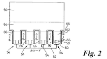
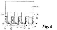
50…P形基板 52…カソード構造
54…MOSFETセル 56…第一N+セル
58…P+セル 60…第二N+セル
62…P形ウェル 64…N形層(レイヤー)
66…トレンチゲート 68…N+セル
70…接点 72…P形ウェル
74…プラーナゲート 76…N形ウェル
78…チャネル 80…P+セル
110…パワーデバイス 112…パワーデバイス
114…トレンチ 116…P形基板
118…N−ドリフト領域 120…アノード接点
122…P+アノード領域 124…カソード接点
126…P+カソードウェル 128…カソード小区域(サブ領域)
130…ゲート 132…N−サンドイッチ領域
140…カソード接点 142…P+ウェル
144…N−ドリフト領域 146…N+カソード小区域(サブ領域)
148…ゲート 150…アノード接点
152…P+アノード領域 154…P形基板
156…底部カソード接点 158…底部P+ウェル
160…底部N−ドリフト領域 162…底部N+カソード小区域(サブ領域)
164…底部ゲート 166…底部アノード接点
168…底部P+アノード領域 170…パワー集積回路
172…ローサイドLIGBTデバイス
174…ハイサイドLIGBTデバイス
176…P+分離ウェル 178…P+分離ウェル
180…金属接点 180…トレンチ
182…トレンチ 184…ハイサイド基盤
186…ローサイド基盤 190…パワー集積回路
192…ローサイドLIGBTデバイス
194…ハイサイドLIGBTデバイス
196…N−サンドイッチ領域 198…P−サンドイッチ領域基板
200…サンドイッチ領域基盤 202…P+分離ウェル
204…P+分離ウェル 206…電気的接点
208…トレンチ 210…トレンチ
Claims (45)
- デバイスの第一部位に横型に設けたソース領域及びドレイン領域と、第一部位から少なくとも第一導電型の基板領域を介して隔てたデバイスの第二部位に設けた少なくとも1つの電流供給セルとを備えてなるパワー半導体デバイス。
- 請求項1のデバイスにおいて、前記第一部位のソース領域及びドレイン領域をLIGBT構造の一部分としてなるパワー半導体デバイス。
- 請求項1又は2のデバイスにおいて、前記電流供給セルをMOS制御構造により制御してなるパワー半導体デバイス。
- 請求項3のデバイスにおいて、前記電流供給セルをMOSFETとしてなるパワー半導体デバイス。
- 請求項3のデバイスにおいて、前記電流供給セルをデバイスの第二部位上に形成したLIGBT構造のソース領域としてなるパワー半導体デバイス。
- 請求項1から3の何れかのデバイスにおいて、前記電流供給セルをダイオード、トランジスタ、又はサイリスタとして作用させてなるパワー半導体デバイス。
- 請求項1から6の何れかのデバイスにおいて、前記デバイスの第二部位に少なくとも1つの第一導電型の電流供給セルを設けてなるパワー半導体デバイス。
- 請求項1から7の何れかのデバイスにおいて、前記電流供給セルを、前記第一導電型の基板領域の下方に配置された少なくとも1つの第二導電型領域を介して第一部位から追加的に隔ててなるパワー半導体デバイス。
- 請求項1から8の何れかのデバイスにおいて、前記ソース領域を基板領域と接触させてなるパワー半導体デバイス。
- 請求項1から8の何れかのデバイスにおいて、前記ソース領域を基板領域と非接触の領域としてなるパワー半導体デバイス。
- 請求項2又は請求項2に従属する請求項3から10の何れかのデバイスにおいて、前記ソース領域に第一導電型のソースウェルに接続されたソース接点とそのソースウェル内に設けた第二導電型のソース小区域とを含め、前記ドレイン領域に第一導電型のドレイン小区域に接続されたドレイン接点を含め、前記ソース領域を第二導電型のドリフト領域を介してドレイン領域から隔て、前記ソース小区域とソースウェルとドレイン領域とに重ねてゲートを設けてなるパワー半導体デバイス。
- 少なくとも1つの論理回路と少なくとも1つのパワー半導体デバイスとを備え、そのパワー半導体デバイスに、デバイスの第一部位に横型に設けたソース領域及びドレイン領域と、少なくとも第一導電型の基板領域を介して第一部位から隔てたデバイスの第二部位に設けた少なくとも1つの電流供給セルとを設けてなるパワー集積回路。
- 請求項12のパワー集積回路において、前記少なくとも1つのパワー半導体デバイスをLIGBTデバイスとしてなるパワー集積回路。
- 請求項12又は13のパワー集積回路において、複数の前記論理回路と複数の前記パワー半導体デバイスとを設けてなるパワー集積回路。
- 請求項14のパワー集積回路において、一対の隣接する前記パワー半導体デバイスを設け、少なくとも前記パワー半導体デバイスの基板領域間の境界部に沿って延びるトレンチを設けて両デバイスを相互に隔ててなるパワー集積回路。
- 請求項15のパワー集積回路において、少なくとも1つの前記パワー半導体デバイスに、その基板領域と接触する第一導電型の深部領域を含めてなるパワー集積回路。
- 請求項15又は16のパワー集積回路において、前記隣接するパワー半導体デバイスの第一部位を相互に離隔する第二導電型の境界領域を設けてなるパワー集積回路。
- 請求項15から17の何れかのパワー集積回路において、前記トレンチを第二導電型の境界領域及び/又は第一導電型の深部領域と接触させることによりパワー半導体デバイスの相互間の電流の流れを実質上遮断してなるパワー集積回路。
- 請求項18のパワー集積回路において、前記一対の隣接するパワー半導体デバイスの基板領域間の境界に、隣接するパワー半導体デバイスのうち少なくとも一方の深部領域又は境界領域を含めてなるパワー集積回路。
- 請求項19のパワー集積回路において、前記境界領域の少なくとも周辺部位に単独又は複数の深部領域を延在させてなるパワー集積回路。
- 請求項16から20の何れかのパワー集積回路において、前記隣接するパワー半導体デバイスの両者にそれぞれ深部領域を設けてなるパワー集積回路。
- 請求項15から21の何れかのパワー集積回路において、前記隣接するパワー半導体デバイスを複数のトレンチによって相互に隔ててなるパワー集積回路。
- 請求項21に従属する請求項22のパワー集積回路において、前記一対のパワー半導体デバイスのうち一方の深部領域に接触させる第一トレンチと、前記一対のパワー半導体デバイスのうち他方の深部領域に隣接する境界領域内に延在させる第二トレンチとを設けてなるパワー集積回路。
- 請求項14から23の何れかのパワー集積回路において、前記一対のパワー半導体デバイスのうち一方をローサイド・デバイスとし他方をハイサイド・デバイスとしてなるパワー集積回路。
- 請求項24のパワー集積回路において、前記ローサイド・デバイスの深部領域に接触させる第一トレンチと、前記ハイサイド・デバイスの深部領域に隣接する境界領域内に延在させる第二トレンチとを設けてなるパワー集積回路。
- 請求項16から25の何れかのパワー集積回路において、前記深部領域をパワー集積回路の外側層と導通可能な分離ウェルとしてなるパワー集積回路。
- 請求項16から26の何れかのパワー集積回路において、前記単独又は複数の深部領域を保護環形状としてなるパワー集積回路。
- 請求項15から27の何れかのパワー集積回路において、前記トレンチを多結晶シリコンその他の半導体物質により充填してなるパワー集積回路。
- 請求項28のパワー集積回路において、前記半導体物質を所定電位又は所定電位差に保持してなるパワー集積回路。
- 請求項15から27の何れかのパワー集積回路において、前記トレンチを絶縁性物質により充填してなるパワー集積回路。
- 請求項30のパワー集積回路において、前記絶縁性物質を酸化物質としてなるパワー集積回路。
- 請求項15から30の何れかのパワー集積回路において、前記トレンチを少なくとも1つのゲートと接続してなるパワー集積回路。
- 複数の論理回路と、それぞれ基板領域上に形成された第一部位を有する少なくとも一対の隣接するパワーデバイスとを備え、前記隣接するパワーデバイスが少なくとも両デバイス間の基板領域間の境界部に沿って延びるトレンチによって相互に隔てられ、前記隣接するパワーデバイスのうち少なくとも一方にデバイスの基板領域と接触する深部領域及び/又は両デバイスの第一部位を分割する第二導電型の境界領域を設け、前記トレンチを深部領域及び/又は境界領域と接触させてパワーデバイス相互間の電流の流れの転位を実質上遮断してなるパワー集積回路又は統合パワーチップ。
- 請求項33の集積回路又はチップにおいて、前記一対の隣接するパワーデバイスの基板領域間の境界に、前記隣接するパワーデバイスのうち少なくとも一方の深部領域又は境界領域を含めてなるパワー集積回路又は統合パワーチップ。
- 請求項34の集積回路又はチップにおいて、前記境界領域の少なくとも周辺部位に単独又は複数の深部領域を延在させてなるパワー集積回路又は統合パワーチップ。
- 請求項33から35の何れかの集積回路又はチップにおいて、前記隣接するパワーデバイスの両者にそれぞれ深部領域を設けてなるパワー集積回路又は統合パワーチップ。
- 請求項33から36の何れかの集積回路又はチップにおいて、前記隣接するパワーデバイスを複数のトレンチによって相互に隔ててなるパワー集積回路又は統合パワーチップ。
- 請求項37の集積回路又はチップにおいて、前記一対のパワーデバイスのうち一方の深部領域に接触させる第一トレンチと、前記一対のパワーデバイスのうち他方の深部領域に隣接する境界領域内に延在させる第二トレンチとを設けてなるパワー集積回路又は統合パワーチップ。
- 請求項33から38の何れかの集積回路又はチップにおいて、前記一対のパワーデバイスのうち一方をローサイド・デバイスとし他方をハイサイド・デバイスとしてなるパワー集積回路又は統合パワーチップ。
- 請求項39の集積回路又はチップにおいて、前記ローサイド・デバイスの深部領域に接触させる第一トレンチと、前記ハイサイド・デバイスの深部領域に隣接する境界領域内に延在させる第二トレンチとを設けてなるパワー集積回路又は統合パワーチップ。
- 請求項33から40の何れかの集積回路又はチップにおいて、前記深部領域をパワー集積回路又は統合パワーチップの外側層と導通可能な分離ウェルとしてなるパワー集積回路又は統合パワーチップ。
- 請求項33から41の何れかの集積回路又はチップにおいて、前記単独又は複数の深部領域を保護環形状としてなるパワー集積回路又は統合パワーチップ。
- 請求項33から42の何れかの集積回路又はチップにおいて、前記トレンチを多結晶シリコンその他の半導体物質により充填してなるパワー集積回路又は統合パワーチップ。
- 請求項33から43の何れかの集積回路又はチップにおいて、前記パワーデバイスをLIGBT、LDMOSその他の横型デバイスとしてなるパワー集積回路又は統合パワーチップ。
- 添付図を参照して明細書において実質的に説明したLIGBTデバイス、パワー集積回路、又は統合パワーチップ。
Applications Claiming Priority (2)
| Application Number | Priority Date | Filing Date | Title |
|---|---|---|---|
| GBGB0520909.3A GB0520909D0 (en) | 2005-10-14 | 2005-10-14 | Power semiconductor devices |
| PCT/GB2006/003833 WO2007042834A2 (en) | 2005-10-14 | 2006-10-16 | Power semiconductor devices |
Publications (2)
| Publication Number | Publication Date |
|---|---|
| JP2009512207A true JP2009512207A (ja) | 2009-03-19 |
| JP2009512207A5 JP2009512207A5 (ja) | 2009-12-03 |
Family
ID=35451744
Family Applications (1)
| Application Number | Title | Priority Date | Filing Date |
|---|---|---|---|
| JP2008535104A Pending JP2009512207A (ja) | 2005-10-14 | 2006-10-16 | パワー半導体デバイス |
Country Status (5)
| Country | Link |
|---|---|
| US (1) | US20090159928A1 (ja) |
| EP (1) | EP1946380A2 (ja) |
| JP (1) | JP2009512207A (ja) |
| GB (1) | GB0520909D0 (ja) |
| WO (1) | WO2007042834A2 (ja) |
Families Citing this family (6)
| Publication number | Priority date | Publication date | Assignee | Title |
|---|---|---|---|---|
| US20110121387A1 (en) * | 2009-11-23 | 2011-05-26 | Francois Hebert | Integrated guarded schottky diode compatible with trench-gate dmos, structure and method |
| US8362555B2 (en) | 2009-11-24 | 2013-01-29 | Intersil Americas Inc. | Voltage converter and systems including same |
| US20110156810A1 (en) * | 2009-12-30 | 2011-06-30 | Intersil Americas Inc. | Integrated dmos and schottky |
| US20110156682A1 (en) * | 2009-12-30 | 2011-06-30 | Dev Alok Girdhar | Voltage converter with integrated schottky device and systems including same |
| US8492225B2 (en) * | 2009-12-30 | 2013-07-23 | Intersil Americas Inc. | Integrated trench guarded schottky diode compatible with powerdie, structure and method |
| KR20120027987A (ko) * | 2010-09-14 | 2012-03-22 | 삼성엘이디 주식회사 | 질화갈륨계 반도체소자 및 그 제조방법 |
Citations (6)
| Publication number | Priority date | Publication date | Assignee | Title |
|---|---|---|---|---|
| JPH07226511A (ja) * | 1994-02-11 | 1995-08-22 | Fuji Electric Co Ltd | 半導体装置 |
| JPH08172194A (ja) * | 1994-09-19 | 1996-07-02 | Internatl Rectifier Corp | 高速igbtデバイス |
| JPH09326441A (ja) * | 1996-06-04 | 1997-12-16 | Toyota Autom Loom Works Ltd | 半導体装置 |
| JPH1065018A (ja) * | 1996-05-14 | 1998-03-06 | Mitsubishi Electric Corp | 半導体装置 |
| JPH11340246A (ja) * | 1998-02-03 | 1999-12-10 | Siemens Ag | パワ―半導体デバイスの製造方法 |
| JPH11354627A (ja) * | 1998-06-05 | 1999-12-24 | Nissan Motor Co Ltd | 半導体集積回路及びその製造方法 |
Family Cites Families (9)
| Publication number | Priority date | Publication date | Assignee | Title |
|---|---|---|---|---|
| SE430450B (sv) * | 1979-04-03 | 1983-11-14 | Asea Ab | Tvapoligt overstromsskydd for inkoppling i en stromforande ledning |
| EP0065346A3 (en) * | 1981-05-20 | 1983-08-31 | Reliance Electric Company | Semiconductor switching device |
| FR2566582B1 (fr) * | 1984-06-22 | 1987-02-20 | Silicium Semiconducteur Ssc | Dispositif bidirectionnel de protection declenche par avalanche |
| FR2574594B1 (fr) * | 1984-12-11 | 1987-01-16 | Silicium Semiconducteur Ssc | Structure integree de triac a commande par diac |
| US5548133A (en) * | 1994-09-19 | 1996-08-20 | International Rectifier Corporation | IGBT with increased ruggedness |
| US6064086A (en) * | 1995-08-24 | 2000-05-16 | Kabushiki Kaisha Toshiba | Semiconductor device having lateral IGBT |
| US5874767A (en) * | 1996-05-14 | 1999-02-23 | Mitsubishi Denki Kabushiki Kaisha | Semiconductor device including a lateral power device |
| GB9921068D0 (en) * | 1999-09-08 | 1999-11-10 | Univ Montfort | Bipolar mosfet device |
| JP4635304B2 (ja) * | 2000-07-12 | 2011-02-23 | 富士電機システムズ株式会社 | 双方向超接合半導体素子およびその製造方法 |
-
2005
- 2005-10-14 GB GBGB0520909.3A patent/GB0520909D0/en not_active Ceased
-
2006
- 2006-10-16 EP EP06794778A patent/EP1946380A2/en not_active Withdrawn
- 2006-10-16 US US12/090,122 patent/US20090159928A1/en not_active Abandoned
- 2006-10-16 WO PCT/GB2006/003833 patent/WO2007042834A2/en active Application Filing
- 2006-10-16 JP JP2008535104A patent/JP2009512207A/ja active Pending
Patent Citations (6)
| Publication number | Priority date | Publication date | Assignee | Title |
|---|---|---|---|---|
| JPH07226511A (ja) * | 1994-02-11 | 1995-08-22 | Fuji Electric Co Ltd | 半導体装置 |
| JPH08172194A (ja) * | 1994-09-19 | 1996-07-02 | Internatl Rectifier Corp | 高速igbtデバイス |
| JPH1065018A (ja) * | 1996-05-14 | 1998-03-06 | Mitsubishi Electric Corp | 半導体装置 |
| JPH09326441A (ja) * | 1996-06-04 | 1997-12-16 | Toyota Autom Loom Works Ltd | 半導体装置 |
| JPH11340246A (ja) * | 1998-02-03 | 1999-12-10 | Siemens Ag | パワ―半導体デバイスの製造方法 |
| JPH11354627A (ja) * | 1998-06-05 | 1999-12-24 | Nissan Motor Co Ltd | 半導体集積回路及びその製造方法 |
Also Published As
| Publication number | Publication date |
|---|---|
| EP1946380A2 (en) | 2008-07-23 |
| GB0520909D0 (en) | 2005-11-23 |
| US20090159928A1 (en) | 2009-06-25 |
| WO2007042834A3 (en) | 2007-06-14 |
| WO2007042834A2 (en) | 2007-04-19 |
Similar Documents
| Publication | Publication Date | Title |
|---|---|---|
| US10157983B2 (en) | Vertical power MOS-gated device with high dopant concentration N-well below P-well and with floating P-islands | |
| US5702961A (en) | Methods of forming insulated gate bipolar transistors having built-in freewheeling diodes and transistors formed thereby | |
| US6900518B2 (en) | Semiconductor device | |
| EP2497116B1 (en) | Power semiconductor devices having selectively doped jfet regions and related methods of forming such devices | |
| JP5357370B2 (ja) | 半導体デバイス | |
| US6303410B1 (en) | Methods of forming power semiconductor devices having T-shaped gate electrodes | |
| US20150008481A1 (en) | Lateral power semiconductor transistors | |
| AU2001290068A1 (en) | Semiconductor Device and Method of Forming a Semiconductor Device | |
| KR20090083424A (ko) | 래치업되지 않는 집적 절연 게이트 양극성 트랜지스터 | |
| JPH10209432A (ja) | 半導体デバイスの改良 | |
| JP2005011846A (ja) | 半導体装置 | |
| US20150187877A1 (en) | Power semiconductor device | |
| US20190006494A1 (en) | Semiconductor device | |
| JP2009512207A (ja) | パワー半導体デバイス | |
| KR101422953B1 (ko) | 전력 반도체 소자 및 그 제조 방법 | |
| KR20150069117A (ko) | 전력 반도체 소자 | |
| JP2000311998A (ja) | 絶縁ゲートターンオフサイリスタ | |
| KR101994728B1 (ko) | 전력 반도체 소자 | |
| JP2005150348A (ja) | 半導体装置 | |
| KR20150076768A (ko) | 전력 반도체 소자 | |
| US11610987B2 (en) | NPNP layered MOS-gated trench device having lowered operating voltage | |
| EP4187615A1 (en) | Npnp layered mos-gated trench device having lowered operating voltage | |
| KR100555444B1 (ko) | 트렌치 게이트형 전력용 반도체 소자 및 그 제조 방법 | |
| JP2023003117A (ja) | 半導体装置 | |
| JPH09213930A (ja) | Misfet制御型半導体装置 |
Legal Events
| Date | Code | Title | Description |
|---|---|---|---|
| A521 | Written amendment |
Free format text: JAPANESE INTERMEDIATE CODE: A523 Effective date: 20091014 |
|
| A621 | Written request for application examination |
Free format text: JAPANESE INTERMEDIATE CODE: A621 Effective date: 20091014 |
|
| A131 | Notification of reasons for refusal |
Free format text: JAPANESE INTERMEDIATE CODE: A131 Effective date: 20120703 |
|
| A977 | Report on retrieval |
Free format text: JAPANESE INTERMEDIATE CODE: A971007 Effective date: 20120705 |
|
| A02 | Decision of refusal |
Free format text: JAPANESE INTERMEDIATE CODE: A02 Effective date: 20121204 |