JP2009512197A - 改良された薄膜ソーラーセル相互接続を形成するシステム及び方法 - Google Patents
改良された薄膜ソーラーセル相互接続を形成するシステム及び方法 Download PDFInfo
- Publication number
- JP2009512197A JP2009512197A JP2008534728A JP2008534728A JP2009512197A JP 2009512197 A JP2009512197 A JP 2009512197A JP 2008534728 A JP2008534728 A JP 2008534728A JP 2008534728 A JP2008534728 A JP 2008534728A JP 2009512197 A JP2009512197 A JP 2009512197A
- Authority
- JP
- Japan
- Prior art keywords
- insulator
- layer
- cut
- interconnect
- forming
- Prior art date
- Legal status (The legal status is an assumption and is not a legal conclusion. Google has not performed a legal analysis and makes no representation as to the accuracy of the status listed.)
- Pending
Links
- 238000000034 method Methods 0.000 title claims abstract description 85
- 239000010409 thin film Substances 0.000 title claims description 22
- 230000008569 process Effects 0.000 claims abstract description 39
- 239000012212 insulator Substances 0.000 claims abstract description 36
- 238000005520 cutting process Methods 0.000 claims abstract description 8
- 238000000151 deposition Methods 0.000 claims description 42
- 239000004020 conductor Substances 0.000 claims description 38
- 238000012545 processing Methods 0.000 claims description 25
- 239000000758 substrate Substances 0.000 claims description 25
- 239000011248 coating agent Substances 0.000 claims description 10
- 238000000576 coating method Methods 0.000 claims description 10
- 239000000463 material Substances 0.000 claims description 8
- 238000009413 insulation Methods 0.000 claims description 2
- 230000008021 deposition Effects 0.000 abstract description 33
- 230000015572 biosynthetic process Effects 0.000 abstract description 3
- 239000004065 semiconductor Substances 0.000 description 20
- 239000011521 glass Substances 0.000 description 13
- 229910052751 metal Inorganic materials 0.000 description 13
- 239000002184 metal Substances 0.000 description 13
- 229920000642 polymer Polymers 0.000 description 10
- 239000000835 fiber Substances 0.000 description 6
- 230000000694 effects Effects 0.000 description 5
- 230000003071 parasitic effect Effects 0.000 description 5
- 238000012546 transfer Methods 0.000 description 5
- 229910021417 amorphous silicon Inorganic materials 0.000 description 4
- 238000010586 diagram Methods 0.000 description 4
- 230000007704 transition Effects 0.000 description 4
- ZOKXTWBITQBERF-UHFFFAOYSA-N Molybdenum Chemical compound [Mo] ZOKXTWBITQBERF-UHFFFAOYSA-N 0.000 description 3
- 239000004642 Polyimide Substances 0.000 description 3
- 230000008901 benefit Effects 0.000 description 3
- 238000004519 manufacturing process Methods 0.000 description 3
- 229910052750 molybdenum Inorganic materials 0.000 description 3
- 239000011733 molybdenum Substances 0.000 description 3
- 229920001721 polyimide Polymers 0.000 description 3
- 238000000926 separation method Methods 0.000 description 3
- 239000007921 spray Substances 0.000 description 3
- 238000001771 vacuum deposition Methods 0.000 description 3
- 229910001218 Gallium arsenide Inorganic materials 0.000 description 2
- KDLHZDBZIXYQEI-UHFFFAOYSA-N Palladium Chemical compound [Pd] KDLHZDBZIXYQEI-UHFFFAOYSA-N 0.000 description 2
- 238000000137 annealing Methods 0.000 description 2
- 230000007547 defect Effects 0.000 description 2
- 238000013461 design Methods 0.000 description 2
- 238000001459 lithography Methods 0.000 description 2
- 238000012986 modification Methods 0.000 description 2
- 230000004048 modification Effects 0.000 description 2
- 229910052759 nickel Inorganic materials 0.000 description 2
- 229920002120 photoresistant polymer Polymers 0.000 description 2
- MARUHZGHZWCEQU-UHFFFAOYSA-N 5-phenyl-2h-tetrazole Chemical compound C1=CC=CC=C1C1=NNN=N1 MARUHZGHZWCEQU-UHFFFAOYSA-N 0.000 description 1
- -1 CIGS Substances 0.000 description 1
- 229910001111 Fine metal Inorganic materials 0.000 description 1
- 229910000530 Gallium indium arsenide Inorganic materials 0.000 description 1
- XUIMIQQOPSSXEZ-UHFFFAOYSA-N Silicon Chemical compound [Si] XUIMIQQOPSSXEZ-UHFFFAOYSA-N 0.000 description 1
- LEVVHYCKPQWKOP-UHFFFAOYSA-N [Si].[Ge] Chemical compound [Si].[Ge] LEVVHYCKPQWKOP-UHFFFAOYSA-N 0.000 description 1
- 229910052782 aluminium Inorganic materials 0.000 description 1
- XAGFODPZIPBFFR-UHFFFAOYSA-N aluminium Chemical compound [Al] XAGFODPZIPBFFR-UHFFFAOYSA-N 0.000 description 1
- 230000005540 biological transmission Effects 0.000 description 1
- 239000003054 catalyst Substances 0.000 description 1
- 230000008859 change Effects 0.000 description 1
- 238000011109 contamination Methods 0.000 description 1
- 238000007796 conventional method Methods 0.000 description 1
- 229910052802 copper Inorganic materials 0.000 description 1
- 239000010949 copper Substances 0.000 description 1
- HVMJUDPAXRRVQO-UHFFFAOYSA-N copper indium Chemical compound [Cu].[In] HVMJUDPAXRRVQO-UHFFFAOYSA-N 0.000 description 1
- 239000013078 crystal Substances 0.000 description 1
- 230000003247 decreasing effect Effects 0.000 description 1
- 238000005137 deposition process Methods 0.000 description 1
- 238000011161 development Methods 0.000 description 1
- 230000009977 dual effect Effects 0.000 description 1
- 239000000428 dust Substances 0.000 description 1
- 239000012776 electronic material Substances 0.000 description 1
- 230000008030 elimination Effects 0.000 description 1
- 238000003379 elimination reaction Methods 0.000 description 1
- 238000005530 etching Methods 0.000 description 1
- 239000011888 foil Substances 0.000 description 1
- 239000011810 insulating material Substances 0.000 description 1
- 229910052745 lead Inorganic materials 0.000 description 1
- 238000012423 maintenance Methods 0.000 description 1
- 238000001465 metallisation Methods 0.000 description 1
- 238000002156 mixing Methods 0.000 description 1
- 230000003287 optical effect Effects 0.000 description 1
- 230000003647 oxidation Effects 0.000 description 1
- 238000007254 oxidation reaction Methods 0.000 description 1
- 229910052763 palladium Inorganic materials 0.000 description 1
- 239000002245 particle Substances 0.000 description 1
- 239000013618 particulate matter Substances 0.000 description 1
- 238000000059 patterning Methods 0.000 description 1
- 238000005240 physical vapour deposition Methods 0.000 description 1
- 230000009467 reduction Effects 0.000 description 1
- 229910052710 silicon Inorganic materials 0.000 description 1
- 239000010703 silicon Substances 0.000 description 1
- 238000004544 sputter deposition Methods 0.000 description 1
- 238000013022 venting Methods 0.000 description 1
Images


Classifications
-
- H—ELECTRICITY
- H01—ELECTRIC ELEMENTS
- H01L—SEMICONDUCTOR DEVICES NOT COVERED BY CLASS H10
- H01L31/00—Semiconductor devices sensitive to infrared radiation, light, electromagnetic radiation of shorter wavelength or corpuscular radiation and specially adapted either for the conversion of the energy of such radiation into electrical energy or for the control of electrical energy by such radiation; Processes or apparatus specially adapted for the manufacture or treatment thereof or of parts thereof; Details thereof
- H01L31/04—Semiconductor devices sensitive to infrared radiation, light, electromagnetic radiation of shorter wavelength or corpuscular radiation and specially adapted either for the conversion of the energy of such radiation into electrical energy or for the control of electrical energy by such radiation; Processes or apparatus specially adapted for the manufacture or treatment thereof or of parts thereof; Details thereof adapted as photovoltaic [PV] conversion devices
- H01L31/042—PV modules or arrays of single PV cells
- H01L31/0445—PV modules or arrays of single PV cells including thin film solar cells, e.g. single thin film a-Si, CIS or CdTe solar cells
- H01L31/046—PV modules composed of a plurality of thin film solar cells deposited on the same substrate
- H01L31/0463—PV modules composed of a plurality of thin film solar cells deposited on the same substrate characterised by special patterning methods to connect the PV cells in a module, e.g. laser cutting of the conductive or active layers
-
- H—ELECTRICITY
- H01—ELECTRIC ELEMENTS
- H01L—SEMICONDUCTOR DEVICES NOT COVERED BY CLASS H10
- H01L31/00—Semiconductor devices sensitive to infrared radiation, light, electromagnetic radiation of shorter wavelength or corpuscular radiation and specially adapted either for the conversion of the energy of such radiation into electrical energy or for the control of electrical energy by such radiation; Processes or apparatus specially adapted for the manufacture or treatment thereof or of parts thereof; Details thereof
- H01L31/04—Semiconductor devices sensitive to infrared radiation, light, electromagnetic radiation of shorter wavelength or corpuscular radiation and specially adapted either for the conversion of the energy of such radiation into electrical energy or for the control of electrical energy by such radiation; Processes or apparatus specially adapted for the manufacture or treatment thereof or of parts thereof; Details thereof adapted as photovoltaic [PV] conversion devices
- H01L31/042—PV modules or arrays of single PV cells
- H01L31/0445—PV modules or arrays of single PV cells including thin film solar cells, e.g. single thin film a-Si, CIS or CdTe solar cells
- H01L31/046—PV modules composed of a plurality of thin film solar cells deposited on the same substrate
- H01L31/0465—PV modules composed of a plurality of thin film solar cells deposited on the same substrate comprising particular structures for the electrical interconnection of adjacent PV cells in the module
-
- Y—GENERAL TAGGING OF NEW TECHNOLOGICAL DEVELOPMENTS; GENERAL TAGGING OF CROSS-SECTIONAL TECHNOLOGIES SPANNING OVER SEVERAL SECTIONS OF THE IPC; TECHNICAL SUBJECTS COVERED BY FORMER USPC CROSS-REFERENCE ART COLLECTIONS [XRACs] AND DIGESTS
- Y02—TECHNOLOGIES OR APPLICATIONS FOR MITIGATION OR ADAPTATION AGAINST CLIMATE CHANGE
- Y02E—REDUCTION OF GREENHOUSE GAS [GHG] EMISSIONS, RELATED TO ENERGY GENERATION, TRANSMISSION OR DISTRIBUTION
- Y02E10/00—Energy generation through renewable energy sources
- Y02E10/50—Photovoltaic [PV] energy
Abstract
【選択図】 図1
Description
Claims (20)
- 薄膜ソーラーセルのための相互接続を形成する方法において、
上記セルの活性層及び導電層のスタックを単一処理シーケンスで堆積するステップと、
上記相互接続を形成するステップと、
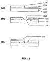
を備えた方法。 - 上記形成するステップは、上記スタックに2つ以上のカットを形成する段階を含み、上記カットのうちの少なくとも1つは、上記スタックを完全に通して下層絶縁体へと達している、請求項1に記載の方法。
- 上記形成するステップは、上記少なくとも1つのカットに隣接し、上記活性層を通して切られ、上記下層絶縁体に導電性レッジを露出させる別のカットを形成する段階を含む、請求項2に記載の方法。
- 上記カットのうちの少なくとも1つを形成するためにレーザーが使用される、請求項2に記載の方法。
- 上記カットのうちの少なくとも1つを形成するために機械的スクライブが使用される、請求項2に記載の方法。
- 上記形成するステップは、上記カットの領域に、絶縁体を堆積し、その後、導体を堆積する段階を更に含む、請求項2に記載の方法。
- 上記形成するステップは、上記カットの領域に、絶縁体を堆積し、その後、導体を堆積する段階を更に含む、請求項3に記載の方法。
- 上記形成するステップは、インクジェット処理を使用して上記相互接続の少なくとも1つの層を形成する段階を含む、請求項1に記載の方法。
- 上記相互接続の接触抵抗を改善するために、上記スタックの上部に付加的な層が堆積される、請求項1に記載の方法。
- 上記絶縁体は、感光性物質である、請求項6に記載の方法。
- 上記絶縁体は、感光性物質である、請求項7に記載の方法。
- 前記絶縁体は、上記スタックが堆積されている基板を通して自己整合形式で露光される、請求項10に記載の方法。
- 上記絶縁体は、上記スタックが堆積されている基板を通して自己整合形式で露光される、請求項11に記載の方法。
- 上記処理シーケンスは、真空内である、請求項1に記載の方法。
- 上記相互接続を形成するステップは、上記活性層を堆積するための上記単一処理シーケンスとは独立した処理で導電性層を堆積する段階を含む、請求項1に記載の方法。
- 上記別に堆積される導電性層は、不透明である、請求項15に記載の方法。
- 上記導電性層は、光導体上に被覆される、請求項16に記載の方法。
- 上記形成するステップは、上記スタックを通してカットを形成する段階を含み、上記カットの第1部分は、上記スタックを完全に通して下層絶縁体まで達し、上記カットの第2部分は、上記活性層を通していて、上記下層絶縁体に導電性レッジを形成している、請求項1に記載の方法。
- レーザーにより行われる上記カットは、上記下層絶縁体の切除により、上記活性層の少なくとも一部分に当接する上記セルの側壁部に絶縁被覆が与えられるようにする、請求項4に記載の方法。
- 上記カットは、レーザーによって行われ、上記下層絶縁体の切除により、上記活性層の少なくとも一部分に当接する上記セルの側壁部に絶縁被覆が与えられるようにする、請求項18に記載の方法。
Applications Claiming Priority (2)
| Application Number | Priority Date | Filing Date | Title |
|---|---|---|---|
| US11/245,620 US20070079866A1 (en) | 2005-10-07 | 2005-10-07 | System and method for making an improved thin film solar cell interconnect |
| PCT/US2006/039212 WO2007044555A2 (en) | 2005-10-07 | 2006-10-06 | System and method for making an improved thin film solar cell interconnect |
Publications (2)
| Publication Number | Publication Date |
|---|---|
| JP2009512197A true JP2009512197A (ja) | 2009-03-19 |
| JP2009512197A5 JP2009512197A5 (ja) | 2009-11-19 |
Family
ID=37910120
Family Applications (1)
| Application Number | Title | Priority Date | Filing Date |
|---|---|---|---|
| JP2008534728A Pending JP2009512197A (ja) | 2005-10-07 | 2006-10-06 | 改良された薄膜ソーラーセル相互接続を形成するシステム及び方法 |
Country Status (7)
| Country | Link |
|---|---|
| US (3) | US20070079866A1 (ja) |
| EP (1) | EP1946434A2 (ja) |
| JP (1) | JP2009512197A (ja) |
| KR (1) | KR20080069597A (ja) |
| CN (1) | CN101496273A (ja) |
| AU (1) | AU2006302366A1 (ja) |
| WO (1) | WO2007044555A2 (ja) |
Cited By (6)
| Publication number | Priority date | Publication date | Assignee | Title |
|---|---|---|---|---|
| WO2010113880A1 (ja) * | 2009-03-31 | 2010-10-07 | 芝浦メカトロニクス株式会社 | 太陽電池の製造方法、太陽電池の製造装置及び太陽電池 |
| JP2013026339A (ja) * | 2011-07-19 | 2013-02-04 | Fujifilm Corp | 薄膜太陽電池およびその製造方法 |
| WO2013069267A1 (ja) * | 2011-11-09 | 2013-05-16 | 富士フイルム株式会社 | 集積化太陽電池の製造方法 |
| JP2015513230A (ja) * | 2012-04-12 | 2015-04-30 | ローベルト ボツシユ ゲゼルシヤフト ミツト ベシユレンクテル ハフツングRobert Bosch Gmbh | 光起電力による薄膜ソーラモジュールならびに該薄膜ソーラモジュールの製造方法 |
| JP2015516110A (ja) * | 2012-05-03 | 2015-06-04 | ネクシスNexcis | 光電池セルの接続のための薄層スタックのレーザエッチング |
| KR101934434B1 (ko) | 2012-10-11 | 2019-01-02 | 엘지이노텍 주식회사 | 태양전지 및 이의 제조 방법 |
Families Citing this family (79)
| Publication number | Priority date | Publication date | Assignee | Title |
|---|---|---|---|---|
| JP4730740B2 (ja) * | 2006-01-30 | 2011-07-20 | 本田技研工業株式会社 | 太陽電池およびその製造方法 |
| US8716591B2 (en) * | 2007-06-20 | 2014-05-06 | Ascent Solar Technologies, Inc. | Array of monolithically integrated thin film photovoltaic cells and associated methods |
| DE102007032283A1 (de) * | 2007-07-11 | 2009-01-15 | Stein, Wilhelm, Dr. | Dünnschichtsolarzellen-Modul und Verfahren zu dessen Herstellung |
| US20090159111A1 (en) * | 2007-12-21 | 2009-06-25 | The Woodside Group Pte. Ltd | Photovoltaic device having a textured metal silicide layer |
| WO2009120824A1 (en) * | 2008-03-26 | 2009-10-01 | E. I. Du Pont De Nemours And Company | High performance anti-spall laminate article |
| EP2257994B1 (en) * | 2008-04-04 | 2018-01-17 | Kuraray America Inc. | Solar cell modules comprising high melt flow poly(vinyl butyral) encapsulants |
| GB2459274A (en) * | 2008-04-15 | 2009-10-21 | Renewable Energy Corp Asa | Wafer based solar panels |
| US20090288701A1 (en) * | 2008-05-23 | 2009-11-26 | E.I.Du Pont De Nemours And Company | Solar cell laminates having colored multi-layer encapsulant sheets |
| CN102047442B (zh) | 2008-06-02 | 2014-05-07 | 纳幕尔杜邦公司 | 具有低雾度包封层的太阳能电池模块 |
| JP2011523211A (ja) * | 2008-06-04 | 2011-08-04 | ソレクサント・コーポレイション | 背面接点を有するモノリシック集積薄膜太陽電池 |
| US20100236607A1 (en) * | 2008-06-12 | 2010-09-23 | General Electric Company | Monolithically integrated solar modules and methods of manufacture |
| TWI420684B (zh) * | 2008-07-04 | 2013-12-21 | Ulvac Inc | 太陽能電池單元之製造方法及太陽能電池單元 |
| US20100031997A1 (en) * | 2008-08-11 | 2010-02-11 | Basol Bulent M | Flexible thin film photovoltaic modules and manufacturing the same |
| US20100047955A1 (en) * | 2008-08-19 | 2010-02-25 | Xunlight Corporation | Interconnection system for photovoltaic modules |
| KR101144808B1 (ko) * | 2008-09-01 | 2012-05-11 | 엘지전자 주식회사 | 박막형 태양전지 제조방법 및 이를 이용한 박막형 태양전지 |
| US7994418B2 (en) * | 2008-09-18 | 2011-08-09 | General Electric Company | Monolithically connected photovoltaic devices on flexible substrates |
| US9379265B2 (en) | 2008-09-29 | 2016-06-28 | Sol Chip Ltd. | Integrated circuit combination of a target integrated circuit, photovoltaic cells and light sensitive diodes connected to enable a self-sufficient light detector device |
| US8952473B2 (en) * | 2008-09-29 | 2015-02-10 | Sol Chip Ltd. | Integrated circuit combination of a target integrated circuit and a plurality of cells connected thereto using the top conductive layer |
| US8921967B2 (en) * | 2008-09-29 | 2014-12-30 | Sol Chip Ltd. | Integrated circuit combination of a target integrated circuit and a plurality of photovoltaic cells connected thereto using the top conductive layer |
| US20100101647A1 (en) * | 2008-10-24 | 2010-04-29 | E.I. Du Pont De Nemours And Company | Non-autoclave lamination process for manufacturing solar cell modules |
| JP6076598B2 (ja) | 2008-10-31 | 2017-02-08 | イー・アイ・デュポン・ドウ・ヌムール・アンド・カンパニーE.I.Du Pont De Nemours And Company | 低ヘイズ封入材を含む太陽電池モジュール |
| US8080727B2 (en) | 2008-11-24 | 2011-12-20 | E. I. Du Pont De Nemours And Company | Solar cell modules comprising an encapsulant sheet of a blend of ethylene copolymers |
| US8084129B2 (en) * | 2008-11-24 | 2011-12-27 | E. I. Du Pont De Nemours And Company | Laminated articles comprising a sheet of a blend of ethylene copolymers |
| US20100154867A1 (en) * | 2008-12-19 | 2010-06-24 | E. I. Du Pont De Nemours And Company | Mechanically reliable solar cell modules |
| JP2010149146A (ja) * | 2008-12-25 | 2010-07-08 | Hitachi High-Technologies Corp | レーザ加工装置 |
| JP5984241B2 (ja) * | 2008-12-31 | 2016-09-06 | イー・アイ・デュポン・ドウ・ヌムール・アンド・カンパニーE.I.Du Pont De Nemours And Company | 低ヘイズ性および高耐湿性を有する封入材シートを含む太陽電池モジュール |
| WO2010085644A1 (en) * | 2009-01-22 | 2010-07-29 | E. I. Du Pont De Nemours And Company | Poly(vinyl butyral) encapsulant comprising chelating agents for solar cell modules |
| JP4773543B2 (ja) * | 2009-04-17 | 2011-09-14 | 昭和シェル石油株式会社 | エッジスペースを備えた太陽電池モジュール |
| EP3621123A1 (en) * | 2009-05-04 | 2020-03-11 | Microlink Devices, Inc. | Assembly techniques for solar cell arrays and solar cells formed therefrom |
| DE102009020482A1 (de) * | 2009-05-08 | 2010-11-11 | Forschungszentrum Jülich GmbH | Verfahren zur Herstellung und Serienverschaltung von photovoltaischen Elementen zu einem Solarmodul und Solarmodul |
| DE102009023125A1 (de) | 2009-05-20 | 2010-11-25 | Universität Stuttgart | Verfahren zur Herstellung seriell verschalteter Solarzellen sowie Vorrichtung zur Durchführung des Verfahrens |
| JP5650737B2 (ja) * | 2009-07-31 | 2015-01-07 | イー・アイ・デュポン・ドウ・ヌムール・アンド・カンパニーE.I.Du Pont De Nemours And Company | 光起電力セル用の架橋性封止材 |
| EP2284892A1 (en) * | 2009-08-12 | 2011-02-16 | Applied Materials, Inc. | Method of manufacturing a semiconductor device module, semiconductor device connecting device, semiconductor device module manufacturing device, semiconductor device module |
| DE102009041905B4 (de) * | 2009-09-20 | 2013-08-22 | Solarion Ag Photovoltaik | Verfahren zur seriellen Verschaltung von Dünnschichtsolarzellen |
| USRE46739E1 (en) | 2009-09-29 | 2018-02-27 | Kyocera Corporation | Photoelectric conversion device and manufacturing method of the same |
| KR101090780B1 (ko) * | 2009-09-30 | 2011-12-08 | 주식회사 티지솔라 | 태양전지 및 그 제조방법 |
| GB2474665B (en) | 2009-10-22 | 2011-10-12 | M Solv Ltd | Method and apparatus for dividing thin film device into separate cells |
| US8865569B2 (en) | 2009-10-22 | 2014-10-21 | M-Solv Ltd. | Method and apparatus for dividing thin film device into separate cells |
| KR101047170B1 (ko) * | 2009-11-30 | 2011-07-07 | 주식회사 티지솔라 | 태양전지 및 그 제조방법 |
| US20110132755A1 (en) * | 2009-12-04 | 2011-06-09 | Kim Woosam | In-line system for manufacturing solar cell |
| KR101072531B1 (ko) * | 2010-01-27 | 2011-10-11 | 주식회사 티지솔라 | 태양전지 및 그 제조방법 |
| KR101037124B1 (ko) | 2010-01-29 | 2011-05-26 | 주식회사 티지솔라 | 태양전지 및 그 제조방법 |
| KR101210168B1 (ko) | 2010-03-24 | 2012-12-07 | 엘지이노텍 주식회사 | 태양광 발전장치 및 이의 제조방법 |
| KR101039149B1 (ko) | 2010-03-31 | 2011-06-07 | 주식회사 티지솔라 | 태양전지 및 그 제조방법 |
| KR101112081B1 (ko) | 2010-05-04 | 2012-02-22 | 주식회사 티지솔라 | 태양전지 및 그 제조방법 |
| US20110303272A1 (en) * | 2010-06-09 | 2011-12-15 | Semiconductor Energy Laboratory Co., Ltd. | Photoelectric Conversion Device and Manufacturing Method Thereof |
| US8642448B2 (en) | 2010-06-22 | 2014-02-04 | Applied Materials, Inc. | Wafer dicing using femtosecond-based laser and plasma etch |
| US8609980B2 (en) | 2010-07-30 | 2013-12-17 | E I Du Pont De Nemours And Company | Cross-linkable ionomeric encapsulants for photovoltaic cells |
| CN101937948B (zh) * | 2010-09-16 | 2012-02-01 | 普尼太阳能(杭州)有限公司 | 一种用于制备聚光薄膜电池的接收器的掩模板 |
| GB2483922B (en) | 2010-09-25 | 2013-11-20 | M Solv Ltd | Method and apparatus for dividing thin film device into separate cells |
| DE202011110968U1 (de) * | 2010-10-15 | 2017-11-16 | Wilhelm Stein | Dünnschichtfotovoltaikmodul |
| US8759197B2 (en) * | 2011-06-15 | 2014-06-24 | Applied Materials, Inc. | Multi-step and asymmetrically shaped laser beam scribing |
| US8703581B2 (en) * | 2011-06-15 | 2014-04-22 | Applied Materials, Inc. | Water soluble mask for substrate dicing by laser and plasma etch |
| US8507363B2 (en) * | 2011-06-15 | 2013-08-13 | Applied Materials, Inc. | Laser and plasma etch wafer dicing using water-soluble die attach film |
| US8557683B2 (en) * | 2011-06-15 | 2013-10-15 | Applied Materials, Inc. | Multi-step and asymmetrically shaped laser beam scribing |
| US8598016B2 (en) * | 2011-06-15 | 2013-12-03 | Applied Materials, Inc. | In-situ deposited mask layer for device singulation by laser scribing and plasma etch |
| US8557682B2 (en) * | 2011-06-15 | 2013-10-15 | Applied Materials, Inc. | Multi-layer mask for substrate dicing by laser and plasma etch |
| GB2492971B (en) | 2011-07-15 | 2013-09-18 | M Solv Ltd | Method and apparatus for dividing thin film device into separate cells |
| US8530263B2 (en) * | 2011-08-10 | 2013-09-10 | Taiwan Semiconductor Manufacturing Co., Ltd. | Superstrate solar cell |
| TW201314921A (zh) * | 2011-09-16 | 2013-04-01 | Axuntek Solar Energy | 太陽能電池模組及其製造方法 |
| TW201316537A (zh) * | 2011-10-04 | 2013-04-16 | Axuntek Solar Energy | 用來製造穿透式太陽能電池模組的方法 |
| KR101219972B1 (ko) * | 2011-11-02 | 2013-01-21 | 엘지이노텍 주식회사 | 태양전지 및 이의 제조방법 |
| US20130133732A1 (en) * | 2011-11-30 | 2013-05-30 | Taiwan Semiconductor Manufacturing Co., Ltd. | Method for forming interconnect in solar cell |
| CN104011877A (zh) * | 2011-12-21 | 2014-08-27 | 陶氏环球技术有限责任公司 | 产生两个或更多个薄膜基互连光伏电池的改进方法 |
| US8845854B2 (en) * | 2012-07-13 | 2014-09-30 | Applied Materials, Inc. | Laser, plasma etch, and backside grind process for wafer dicing |
| KR101382880B1 (ko) * | 2012-07-31 | 2014-04-09 | 엘지이노텍 주식회사 | 태양광 발전장치 및 이의 제조방법 |
| JP6537973B2 (ja) | 2012-12-19 | 2019-07-03 | イー・アイ・デュポン・ドウ・ヌムール・アンド・カンパニーE.I.Du Pont De Nemours And Company | 架橋性酸コポリマー組成物およびガラスラミネートでのその使用 |
| WO2014152556A1 (en) * | 2013-03-15 | 2014-09-25 | First Solar, Inc. | Photovoltaic device interconnection and method of manufacturing |
| CN103618030B (zh) * | 2013-11-28 | 2016-03-09 | 上海空间电源研究所 | 柔性pi衬底cigs薄膜电池激光刻蚀单体集成组件的方法 |
| US20150263197A1 (en) * | 2014-03-14 | 2015-09-17 | First Solar, Inc. | Photovoltaic device interconnection and method of manufacturing |
| US20150325729A1 (en) | 2014-05-09 | 2015-11-12 | E. I. Du Pont De Nemours And Company | Encapsulant composition comprising a copolymer of ethylene, vinyl acetate and a third comonomer |
| DE102014111649A1 (de) * | 2014-08-14 | 2016-02-18 | Thyssenkrupp Ag | Unterwasserfahrzeug, Verfahren zum Aufnehmen einer Last vom Meeresgrund und ein Verfahren zum Absetzen einer Last am Meeresgrund |
| NL2014040B1 (en) * | 2014-12-23 | 2016-10-12 | Stichting Energieonderzoek Centrum Nederland | Method of making a curent collecting grid for solar cells. |
| CN104766907A (zh) * | 2015-04-09 | 2015-07-08 | 山东禹城汉能薄膜太阳能有限公司 | 柔性cigs薄膜太阳能电池的连接方法 |
| NL2016708B1 (en) * | 2016-04-29 | 2017-11-16 | Stichting Energieonderzoek Centrum Nederland | A method for manufacturing interconnected solar cells and such interconnected solar cells. |
| BR112020017145A2 (pt) | 2018-03-08 | 2020-12-22 | Performance Materials Na, Inc. | Módulo fotovoltaico, e, método para reduzir a degradação induzida por potencial de um módulo fotovoltaico. |
| GB2575792B (en) | 2018-07-20 | 2021-11-03 | Dyson Technology Ltd | Stack for an energy storage device |
| CN111490107A (zh) * | 2019-01-25 | 2020-08-04 | 神华(北京)光伏科技研发有限公司 | 薄膜太阳电池及薄膜太阳电池的制备方法 |
| CN112786737A (zh) * | 2021-01-26 | 2021-05-11 | 凯盛光伏材料有限公司 | Cigs薄膜太阳能电池组件及其刻划方法 |
Citations (6)
| Publication number | Priority date | Publication date | Assignee | Title |
|---|---|---|---|---|
| JPS6284569A (ja) * | 1985-10-08 | 1987-04-18 | Sanyo Electric Co Ltd | 光起電力装置の製造方法 |
| US4879251A (en) * | 1987-08-20 | 1989-11-07 | Siemens Aktiengesellschaft | Method of making series-connected, thin-film solar module formed of crystalline silicon |
| JPH03250771A (ja) * | 1990-02-28 | 1991-11-08 | Sanyo Electric Co Ltd | 光起電力装置の製造方法 |
| JPH04116986A (ja) * | 1990-09-07 | 1992-04-17 | Canon Inc | 集積化太陽電池 |
| JPH08139351A (ja) * | 1994-11-08 | 1996-05-31 | Matsushita Electric Ind Co Ltd | 太陽電池モジュールの作製方法及びその作製装置 |
| US6690041B2 (en) * | 2002-05-14 | 2004-02-10 | Global Solar Energy, Inc. | Monolithically integrated diodes in thin-film photovoltaic devices |
Family Cites Families (30)
| Publication number | Priority date | Publication date | Assignee | Title |
|---|---|---|---|---|
| US4312114A (en) * | 1977-02-24 | 1982-01-26 | The United States Of America As Represented By The Secretary Of The Navy | Method of preparing a thin-film, single-crystal photovoltaic detector |
| US4262411A (en) * | 1977-09-08 | 1981-04-21 | Photon Power, Inc. | Method of making a solar cell array |
| US4278473A (en) * | 1979-08-24 | 1981-07-14 | Varian Associates, Inc. | Monolithic series-connected solar cell |
| US4377723A (en) * | 1980-05-02 | 1983-03-22 | The University Of Delaware | High efficiency thin-film multiple-gap photovoltaic device |
| US4383130A (en) * | 1981-05-04 | 1983-05-10 | Alpha Solarco Inc. | Solar energy cell and method of manufacture |
| US4479027A (en) * | 1982-09-24 | 1984-10-23 | Todorof William J | Multi-layer thin-film, flexible silicon alloy photovoltaic cell |
| US4604791A (en) * | 1982-09-24 | 1986-08-12 | Todorof William J | Method for producing multi-layer, thin-film, flexible silicon alloy photovoltaic cells |
| US4595791A (en) * | 1985-01-29 | 1986-06-17 | The Standard Oil Company | Thin-film photovoltaic devices incorporating current collector grid and method of making |
| US4754544A (en) * | 1985-01-30 | 1988-07-05 | Energy Conversion Devices, Inc. | Extremely lightweight, flexible semiconductor device arrays |
| US4667058A (en) * | 1985-07-01 | 1987-05-19 | Solarex Corporation | Method of fabricating electrically isolated photovoltaic modules arrayed on a substrate and product obtained thereby |
| US4695674A (en) * | 1985-08-30 | 1987-09-22 | The Standard Oil Company | Preformed, thin-film front contact current collector grid for photovoltaic cells |
| US4781766A (en) * | 1985-10-30 | 1988-11-01 | Astrosystems, Inc. | Fault tolerant thin-film photovoltaic cell and method |
| US4677250A (en) * | 1985-10-30 | 1987-06-30 | Astrosystems, Inc. | Fault tolerant thin-film photovoltaic cell |
| US4772564A (en) * | 1985-10-30 | 1988-09-20 | Astrosystems, Inc. | Fault tolerant thin-film photovoltaic cell fabrication process |
| US5501744A (en) * | 1992-01-13 | 1996-03-26 | Photon Energy, Inc. | Photovoltaic cell having a p-type polycrystalline layer with large crystals |
| DE4324320B4 (de) * | 1992-07-24 | 2006-08-31 | Fuji Electric Co., Ltd., Kawasaki | Verfahren und Vorrichtung zur Herstellung einer als dünne Schicht ausgebildeten fotovoltaischen Umwandlungsvorrichtung |
| DE4241045C1 (de) * | 1992-12-05 | 1994-05-26 | Bosch Gmbh Robert | Verfahren zum anisotropen Ätzen von Silicium |
| US5306646A (en) * | 1992-12-23 | 1994-04-26 | Martin Marietta Energy Systems, Inc. | Method for producing textured substrates for thin-film photovoltaic cells |
| US5730852A (en) * | 1995-09-25 | 1998-03-24 | Davis, Joseph & Negley | Preparation of cuxinygazsen (X=0-2, Y=0-2, Z=0-2, N=0-3) precursor films by electrodeposition for fabricating high efficiency solar cells |
| DE19736370C2 (de) * | 1997-08-21 | 2001-12-06 | Bosch Gmbh Robert | Verfahren zum anisotropen Ätzen von Silizium |
| EP1045454A4 (en) * | 1998-07-27 | 2001-10-24 | Citizen Watch Co Ltd | SOLAR CELL AND PRODUCTION METHOD, AND MASK FOR PHOTOLITHOGRAPHY FOR PRODUCING THE SOLAR CELL |
| US6455347B1 (en) * | 1999-06-14 | 2002-09-24 | Kaneka Corporation | Method of fabricating thin-film photovoltaic module |
| AU777360B2 (en) * | 1999-10-27 | 2004-10-14 | Kaneka Corporation | Method of producing a thin-film photovoltaic device |
| US6310281B1 (en) * | 2000-03-16 | 2001-10-30 | Global Solar Energy, Inc. | Thin-film, flexible photovoltaic module |
| US6372538B1 (en) * | 2000-03-16 | 2002-04-16 | University Of Delaware | Fabrication of thin-film, flexible photovoltaic module |
| US6423565B1 (en) * | 2000-05-30 | 2002-07-23 | Kurt L. Barth | Apparatus and processes for the massproduction of photovotaic modules |
| JP4006994B2 (ja) * | 2001-12-18 | 2007-11-14 | 株式会社リコー | 立体構造体の加工方法、立体形状品の製造方法及び立体構造体 |
| US7259321B2 (en) * | 2002-01-07 | 2007-08-21 | Bp Corporation North America Inc. | Method of manufacturing thin film photovoltaic modules |
| JP4465429B2 (ja) * | 2002-02-21 | 2010-05-19 | 株式会社リコー | レーザ加工方法 |
| JP2006013403A (ja) * | 2004-06-29 | 2006-01-12 | Sanyo Electric Co Ltd | 太陽電池、太陽電池モジュール、その製造方法およびその修復方法 |
-
2005
- 2005-10-07 US US11/245,620 patent/US20070079866A1/en not_active Abandoned
-
2006
- 2006-10-06 JP JP2008534728A patent/JP2009512197A/ja active Pending
- 2006-10-06 CN CNA2006800393288A patent/CN101496273A/zh active Pending
- 2006-10-06 WO PCT/US2006/039212 patent/WO2007044555A2/en active Application Filing
- 2006-10-06 EP EP06816441A patent/EP1946434A2/en not_active Withdrawn
- 2006-10-06 AU AU2006302366A patent/AU2006302366A1/en not_active Abandoned
- 2006-10-06 KR KR1020087010953A patent/KR20080069597A/ko not_active Application Discontinuation
-
2008
- 2008-09-19 US US12/234,509 patent/US20090007957A1/en not_active Abandoned
- 2008-09-19 US US12/234,524 patent/US20090014052A1/en not_active Abandoned
Patent Citations (6)
| Publication number | Priority date | Publication date | Assignee | Title |
|---|---|---|---|---|
| JPS6284569A (ja) * | 1985-10-08 | 1987-04-18 | Sanyo Electric Co Ltd | 光起電力装置の製造方法 |
| US4879251A (en) * | 1987-08-20 | 1989-11-07 | Siemens Aktiengesellschaft | Method of making series-connected, thin-film solar module formed of crystalline silicon |
| JPH03250771A (ja) * | 1990-02-28 | 1991-11-08 | Sanyo Electric Co Ltd | 光起電力装置の製造方法 |
| JPH04116986A (ja) * | 1990-09-07 | 1992-04-17 | Canon Inc | 集積化太陽電池 |
| JPH08139351A (ja) * | 1994-11-08 | 1996-05-31 | Matsushita Electric Ind Co Ltd | 太陽電池モジュールの作製方法及びその作製装置 |
| US6690041B2 (en) * | 2002-05-14 | 2004-02-10 | Global Solar Energy, Inc. | Monolithically integrated diodes in thin-film photovoltaic devices |
Cited By (6)
| Publication number | Priority date | Publication date | Assignee | Title |
|---|---|---|---|---|
| WO2010113880A1 (ja) * | 2009-03-31 | 2010-10-07 | 芝浦メカトロニクス株式会社 | 太陽電池の製造方法、太陽電池の製造装置及び太陽電池 |
| JP2013026339A (ja) * | 2011-07-19 | 2013-02-04 | Fujifilm Corp | 薄膜太陽電池およびその製造方法 |
| WO2013069267A1 (ja) * | 2011-11-09 | 2013-05-16 | 富士フイルム株式会社 | 集積化太陽電池の製造方法 |
| JP2015513230A (ja) * | 2012-04-12 | 2015-04-30 | ローベルト ボツシユ ゲゼルシヤフト ミツト ベシユレンクテル ハフツングRobert Bosch Gmbh | 光起電力による薄膜ソーラモジュールならびに該薄膜ソーラモジュールの製造方法 |
| JP2015516110A (ja) * | 2012-05-03 | 2015-06-04 | ネクシスNexcis | 光電池セルの接続のための薄層スタックのレーザエッチング |
| KR101934434B1 (ko) | 2012-10-11 | 2019-01-02 | 엘지이노텍 주식회사 | 태양전지 및 이의 제조 방법 |
Also Published As
| Publication number | Publication date |
|---|---|
| US20070079866A1 (en) | 2007-04-12 |
| US20090014052A1 (en) | 2009-01-15 |
| US20090007957A1 (en) | 2009-01-08 |
| AU2006302366A1 (en) | 2007-04-19 |
| EP1946434A2 (en) | 2008-07-23 |
| KR20080069597A (ko) | 2008-07-28 |
| CN101496273A (zh) | 2009-07-29 |
| WO2007044555A2 (en) | 2007-04-19 |
| WO2007044555A3 (en) | 2009-04-23 |
Similar Documents
| Publication | Publication Date | Title |
|---|---|---|
| JP2009512197A (ja) | 改良された薄膜ソーラーセル相互接続を形成するシステム及び方法 | |
| US7718347B2 (en) | Method for making an improved thin film solar cell interconnect using etch and deposition process | |
| US8846419B2 (en) | Thin layer solar cell module and method for producing it | |
| US8309390B2 (en) | Method of manufacturing a photovoltaic device and system for patterning an object | |
| US7547570B2 (en) | Method for forming thin film photovoltaic interconnects using self-aligned process | |
| KR100656738B1 (ko) | 집적형 박막 태양전지 및 그 제조 방법 | |
| US9893221B2 (en) | Solar cell and method of fabricating the same | |
| US7868248B2 (en) | Chain link metal interconnect structure | |
| US20100229914A1 (en) | Solar cells with shunt resistance | |
| US20070227578A1 (en) | Method for patterning a photovoltaic device comprising CIGS material using an etch process | |
| US7547569B2 (en) | Method for patterning Mo layer in a photovoltaic device comprising CIGS material using an etch process | |
| WO1993023880A1 (en) | Monolithic, parallel connected photovoltaic array and method for its manufacture | |
| KR20060100174A (ko) | 집적형 박막 태양전지 및 그 제조 방법 | |
| KR20100023759A (ko) | 태양 전지 기판 및 제조 방법 | |
| JP2000315809A (ja) | 集積型薄膜太陽電池の製造方法およびパターニング装置 | |
| US8912617B2 (en) | Method for making semiconductor light detection devices | |
| KR20110035733A (ko) | 태양전지 및 이의 제조방법 | |
| JP2005521247A (ja) | 薄膜層の自己調節式直列回路とその作製方法 | |
| US20140045293A1 (en) | Fabrication of interconnected thin-film concentrator cells using shadow masks | |
| US11444217B2 (en) | Method for producing a thin-film solar module | |
| EP4318604A1 (en) | Thin film photovoltaic devices and method of manufacturing them | |
| JP5440439B2 (ja) | 薄膜光電変換装置の製造方法 | |
| JPS6030184A (ja) | 光起電力装置の製造方法 |
Legal Events
| Date | Code | Title | Description |
|---|---|---|---|
| A521 | Written amendment |
Free format text: JAPANESE INTERMEDIATE CODE: A523 Effective date: 20091002 |
|
| A621 | Written request for application examination |
Free format text: JAPANESE INTERMEDIATE CODE: A621 Effective date: 20091002 |
|
| A977 | Report on retrieval |
Free format text: JAPANESE INTERMEDIATE CODE: A971007 Effective date: 20111226 |
|
| A131 | Notification of reasons for refusal |
Free format text: JAPANESE INTERMEDIATE CODE: A131 Effective date: 20120110 |
|
| A02 | Decision of refusal |
Free format text: JAPANESE INTERMEDIATE CODE: A02 Effective date: 20120605 |