JP2009081407A - Method for manufacturing light-emitting diode, light-emitting diode, and lamp - Google Patents
Method for manufacturing light-emitting diode, light-emitting diode, and lamp Download PDFInfo
- Publication number
- JP2009081407A JP2009081407A JP2007251479A JP2007251479A JP2009081407A JP 2009081407 A JP2009081407 A JP 2009081407A JP 2007251479 A JP2007251479 A JP 2007251479A JP 2007251479 A JP2007251479 A JP 2007251479A JP 2009081407 A JP2009081407 A JP 2009081407A
- Authority
- JP
- Japan
- Prior art keywords
- layer
- emitting diode
- plating
- resist layer
- light emitting
- Prior art date
- Legal status (The legal status is an assumption and is not a legal conclusion. Google has not performed a legal analysis and makes no representation as to the accuracy of the status listed.)
- Granted
Links
Images


Classifications
-
- H—ELECTRICITY
- H01—ELECTRIC ELEMENTS
- H01L—SEMICONDUCTOR DEVICES NOT COVERED BY CLASS H10
- H01L2224/00—Indexing scheme for arrangements for connecting or disconnecting semiconductor or solid-state bodies and methods related thereto as covered by H01L24/00
- H01L2224/01—Means for bonding being attached to, or being formed on, the surface to be connected, e.g. chip-to-package, die-attach, "first-level" interconnects; Manufacturing methods related thereto
- H01L2224/42—Wire connectors; Manufacturing methods related thereto
- H01L2224/47—Structure, shape, material or disposition of the wire connectors after the connecting process
- H01L2224/48—Structure, shape, material or disposition of the wire connectors after the connecting process of an individual wire connector
- H01L2224/4805—Shape
- H01L2224/4809—Loop shape
- H01L2224/48091—Arched
-
- H—ELECTRICITY
- H01—ELECTRIC ELEMENTS
- H01L—SEMICONDUCTOR DEVICES NOT COVERED BY CLASS H10
- H01L2224/00—Indexing scheme for arrangements for connecting or disconnecting semiconductor or solid-state bodies and methods related thereto as covered by H01L24/00
- H01L2224/01—Means for bonding being attached to, or being formed on, the surface to be connected, e.g. chip-to-package, die-attach, "first-level" interconnects; Manufacturing methods related thereto
- H01L2224/42—Wire connectors; Manufacturing methods related thereto
- H01L2224/47—Structure, shape, material or disposition of the wire connectors after the connecting process
- H01L2224/48—Structure, shape, material or disposition of the wire connectors after the connecting process of an individual wire connector
- H01L2224/481—Disposition
- H01L2224/48151—Connecting between a semiconductor or solid-state body and an item not being a semiconductor or solid-state body, e.g. chip-to-substrate, chip-to-passive
- H01L2224/48221—Connecting between a semiconductor or solid-state body and an item not being a semiconductor or solid-state body, e.g. chip-to-substrate, chip-to-passive the body and the item being stacked
- H01L2224/48245—Connecting between a semiconductor or solid-state body and an item not being a semiconductor or solid-state body, e.g. chip-to-substrate, chip-to-passive the body and the item being stacked the item being metallic
- H01L2224/48247—Connecting between a semiconductor or solid-state body and an item not being a semiconductor or solid-state body, e.g. chip-to-substrate, chip-to-passive the body and the item being stacked the item being metallic connecting the wire to a bond pad of the item
Landscapes
- Led Device Packages (AREA)
- Led Devices (AREA)
Abstract
Description
本発明は、発光ダイオードの製造方法及び発光ダイオード、並びにランプに関するものである。 The present invention relates to a light emitting diode manufacturing method, a light emitting diode, and a lamp.
III族窒化物半導体は、可視光から紫外光領域の範囲に相当するエネルギーの直接遷移型のバンドギャップを有し、発光効率に優れていることから、発光ダイオード(LED)やレーザダイオード(LD)等の発光素子として製品化され、各種用途で使用されている。また、電子デバイスに用いた場合でも、III族窒化物半導体は、従来のIII−V族化合物半導体を用いた場合に比べ、優れた特性が得られるポテンシャルを有している。 Group III nitride semiconductors have a direct transition type band gap of energy corresponding to the range from visible light to ultraviolet light, and are excellent in luminous efficiency. Therefore, light emitting diodes (LEDs) and laser diodes (LDs) It is commercialized as a light emitting device such as, and is used in various applications. Even when used in an electronic device, the group III nitride semiconductor has a potential for obtaining excellent characteristics as compared with the case of using a conventional group III-V compound semiconductor.
一般に、III族窒化物半導体は、トリメチルガリウム、トリメチルアルミニウムおよびアンモニアを原料として、有機金属化学気相成長(MOCVD)法によって製造されている。MOCVD法は、キャリアガスに原料の蒸気を含ませて基板表面に運搬し、加熱された基板との反応で原料を分解させることにより、結晶を成長させる方法である。 In general, a group III nitride semiconductor is manufactured by metal organic chemical vapor deposition (MOCVD) using trimethyl gallium, trimethyl aluminum, and ammonia as raw materials. The MOCVD method is a method in which a vapor of a raw material is contained in a carrier gas and transported to the substrate surface, and the raw material is decomposed by reaction with a heated substrate to grow crystals.
基板には例えばサファイア等の絶縁性基板の他、炭化ケイ素、シリコン、酸化亜鉛、ガリウム砒素等の導電性基板が使用できることが知られているが、III族窒化物半導体と完全に格子整合する基板は未だ開発されておらず、現在のところ、格子定数が10%以上も異なるサファイアの上にIII族窒化物半導体層を強制的に成長させた青色LED素子が実用化されている。 As the substrate, it is known that a conductive substrate such as silicon carbide, silicon, zinc oxide, gallium arsenide, etc. can be used in addition to an insulating substrate such as sapphire, but a substrate perfectly lattice-matched with a group III nitride semiconductor. Has not yet been developed, and at present, a blue LED element in which a group III nitride semiconductor layer is forcibly grown on sapphire having a lattice constant different by 10% or more has been put into practical use.
従来の青色LED素子は、基本的にサファイア基板の上にIII族窒化物半導体よりなるn型半導体層と発光層とp型半導体層とが順に積層されたダブルへテロ構造を有している。前記のようにサファイアは絶縁性であり基板側から電極を取り出すことができないので、同一のIII族窒化物半導体層表面にp型電極とn型電極とが設けられた、いわゆるフェイスアップ方式や、フリップチップ方式の素子とされている。 A conventional blue LED element basically has a double hetero structure in which an n-type semiconductor layer made of a group III nitride semiconductor, a light emitting layer, and a p-type semiconductor layer are sequentially laminated on a sapphire substrate. As described above, since sapphire is insulative and the electrode cannot be taken out from the substrate side, a so-called face-up method in which a p-type electrode and an n-type electrode are provided on the same group III nitride semiconductor layer surface, It is a flip chip type element.
しかしながら、サファイアを基板とする従来のフェイスアップ方式またはフリップチップ方式の素子にはいくつかの問題点がある。まず、第一に、p型電極とn型電極とが水平方向に並んでいるため電流が水平方向に流れ、その結果、電流密度が局部的に高くなりチップが発熱する。第二にサファイアという非常に硬く、劈開性のない基板を使用しているので、チップ化するのに高度な技術を必要とする。第3に、サファイアは熱伝導性が比較的低いので、III族窒化物半導体層において発生した熱を効率よく放熱できない。 However, there are some problems in the conventional face-up type or flip-chip type device using sapphire as a substrate. First, since the p-type electrode and the n-type electrode are arranged in the horizontal direction, the current flows in the horizontal direction. As a result, the current density is locally increased and the chip generates heat. Secondly, since a very hard and non-cleavable substrate called sapphire is used, advanced technology is required to make a chip. Third, since sapphire has a relatively low thermal conductivity, it cannot efficiently dissipate heat generated in the group III nitride semiconductor layer.
上記問題を回避するため、下記特許文献1には、メッキ層上にIII族窒化物半導体層が形成された上下電極構造の発光ダイオードを製造する方法が開示されている。すなわち、特許文献1には、サファイア基板上にn型半導体層、発光層及びp型半導体層を順次積層してIII族窒化物半導体層を形成するとともに、p型半導体層の一面にp型オーミック電極を形成し、次いで、p型オーミック電極上にシード層を形成してからシード層上にフォトレジストを格子状に形成し、次いで、シード層及びフォトレジストを覆うようにメッキ層を形成し、次いで、サファイア基板を除去してからn型半導体層にn型オーミック電極を形成し、最後に、フォトレジストを除去してからウェーハをダイシングする上下電極構造の発光ダイオードの製造方法が開示されている。
しかしながら、上記のような特許文献1に記載の方法では、分割された各素子がバラバラに散らばった状態となってしまい、作業効率ひいては生産効率が低下する虞がある。
In order to avoid the above problem,
However, in the method described in
また、下記特許文献2には、レーザスクライブ法を用いてウェーハのダイシングを行なうことにより、III族窒化物半導体層が形成された上下電極構造の発光ダイオードを製造する方法が開示されている。すなわち、特許文献2には、III族窒化物半導体層が形成された上下電極構造の発光ダイオードの製造工程において、サファイア基板上にIII族窒化物半導体層を形成し、次いで、半導体層上に保護層を形成してこの上にフォトレジストを格子状に形成した後、III族窒化物半導体層をエッチングによって複数に分割し、次いで、フォトレジストを除去して導電性基板を取り付けた後にサファイア基板を除去し、最後にウェーハをレーザスクライブでダイシングすることにより、複数の上下電極構造の発光ダイオードを得る方法が開示されている。
しかしながら、特許文献2に記載のダイオードの製造方法のようにレーザスクライブでダイシングを行う場合、切断する箇所の導電性基板の厚さを60μm以下の薄肉に形成する必要がある。このため、サファイア基板の除去後のウェーハが撓み易くなり、取り扱いが難しいという問題がある。また、ウェーハの撓みによるストレスのため、エピタキシャル層にダメージが生じてしまい、リークを起こし易くなるという問題がある。
However, when dicing is performed by laser scribing as in the diode manufacturing method described in
一般に、発光ダイオードの製造工程においては、ウェーハのダイシングを行なった際の、1ウェーハ当たりの発光ダイオードとしての分割数が多数となるため、分割後の素子を適正に管理する必要がある。
しかしながら、上記特許文献1の発光ダイオードの製造方法では、ウェーハをダイシングして分割した後、各素子がダイシング用テーブル上に散らばった状態となる場合があるため、管理に多大な手間を要する。このため、製造効率が低下するとともに、分割後の管理を適切に行なわなかった場合には素子を傷めてしまい、ひいては歩留まりが低下する虞があった。また、上記特許文献2の発光ダイオードの製造方法では、上述したように、導電性基板が薄くハンドリング時に撓み易いため、エピタキシャルにダメージが生じ、リークを起こし易いという問題があった。
In general, in the manufacturing process of light emitting diodes, when the wafer is diced, the number of divisions as light emitting diodes per wafer is large, and thus it is necessary to properly manage the divided elements.
However, in the method of manufacturing the light emitting diode of
本発明は上記事情に鑑みてなされたものであり、ウェーハの取り扱い性を向上させるとともに、ダイシングによる素子分割時の管理を容易にし、生産効率を向上させることが可能な、上下電極構造の発光ダイオードの製造方法の提供を目的とする。 The present invention has been made in view of the above circumstances, and improves the handleability of the wafer, facilitates the management at the time of element division by dicing, and can improve the production efficiency. It aims at providing the manufacturing method of this.
上記の目的を達成するために、本発明は以下の構成を採用した。
[1] 基板上に、n型半導体層、発光層、p型半導体層を順次積層した後、分離溝を形成し、さらにp型電極層を順次積層して複数の化合物半導体層を形成する積層工程と、前記複数の化合物半導体層の各々の間の前記分離溝に、平坦化用レジスト層を埋め込むように形成する平坦化工程と、前記複数の化合物半導体層及び前記平坦化用レジスト層の上にシード層を形成するシード層形成工程と、前記シード層上に、前記平坦化用レジスト層に沿う分離用レジスト層を包含し、該分離用レジスト層によって一部が分断されてなるメッキ層を形成するとともに、該メッキ層に仮貼付基板を貼り付けるメッキ工程と、前記基板を前記複数の化合物半導体層及び前記平坦化用レジスト層から剥離して、前記複数の化合物半導体層に備えられる前記n型半導体層の光取出面を露出させるとともに、平坦化用レジスト層及び分離用レジスト層を除去する除去工程と、前記複数の化合物半導体層に備えられるn型半導体層上にn型電極層を形成する電極形成工程と、前記仮貼付基板を除去する仮貼付基板除去工程と、前記メッキ層の内、前記分離用レジスト層によって分断された部分に沿って、前記メッキ層を切断するダイシング工程と、を具備してなることを特徴とする発光ダイオードの製造方法。
[2] 前記メッキ工程において、前記シード層上に分離用レジスト層を形成し、前記メッキ層を前記分離用レジスト層よりも厚く形成することにより、前記分離用レジスト層によって一部が分断されてなるメッキ層を形成することを特徴とする前項[1]に記載の発光ダイオードの製造方法。
[3] 前記メッキ工程において、前記シード層上に第1メッキ層を形成した後、該第1メッキ層上に分離用レジスト層を形成するとともに、該分離用レジスト層と同じ厚さ寸法の第2メッキ層を形成することにより、前記分離用レジスト層によって一部が分断されてなるメッキ層を形成することを特徴とする前項[1]に記載の発光ダイオードの製造方法。
[4] 前記除去工程は、前記メッキ層に包含される前記分離用レジスト層を除去することにより、前記メッキ層の内、前記分離用レジスト層によって分断された部分に分断溝を形成することを特徴とする前項[1]〜[3]の何れか1項に記載の発光ダイオードの製造方法。
[5] 前記除去工程と前記電極形成工程との間において、前記複数の化合物半導体層の周囲面に、保護用の絶縁膜を形成する絶縁膜形成工程を設けることを特徴とする前項[1]〜[4]の何れか1項に記載の発光ダイオードの製造方法。
[6] 前記絶縁膜形成工程と前記電極形成工程との間において、前記n型半導体層の前記光取出面を粗面化する粗面化工程を設けることを特徴とする前項[5]に記載の発光ダイオードの製造方法。
[7] 前項[1]〜[6]の何れか1項に記載の製造方法で得られる発光ダイオード。
[8] 前項[7]に記載の発光ダイオードが用いられてなるランプ。
In order to achieve the above object, the present invention employs the following configuration.
[1] A stack in which an n-type semiconductor layer, a light emitting layer, and a p-type semiconductor layer are sequentially stacked on a substrate, a separation groove is formed, and a p-type electrode layer is sequentially stacked to form a plurality of compound semiconductor layers. A planarization step of embedding a planarization resist layer in the separation groove between each of the plurality of compound semiconductor layers, and a plurality of the compound semiconductor layers and the planarization resist layer. A seed layer forming step of forming a seed layer on the seed layer; and a plating layer including a separation resist layer along the planarization resist layer on the seed layer, and a part of which is separated by the separation resist layer. A plating step of forming and temporarily attaching a temporary attachment substrate to the plating layer; and removing the substrate from the plurality of compound semiconductor layers and the planarizing resist layer to provide the n in the plurality of compound semiconductor layers And removing the planarizing resist layer and the separating resist layer, and forming an n-type electrode layer on the n-type semiconductor layers provided in the plurality of compound semiconductor layers An electrode forming step, a temporary sticking substrate removing step for removing the temporary sticking substrate, a dicing step for cutting the plating layer along a portion of the plating layer divided by the resist layer for separation, A method for manufacturing a light emitting diode, comprising:
[2] In the plating step, a separation resist layer is formed on the seed layer, and the plating layer is formed to be thicker than the separation resist layer, so that a part is divided by the separation resist layer. The method for producing a light-emitting diode according to [1], wherein a plating layer is formed.
[3] In the plating step, after forming a first plating layer on the seed layer, a separation resist layer is formed on the first plating layer, and a first resist layer having the same thickness as the separation resist layer is formed. 2. The method for manufacturing a light-emitting diode according to [1], wherein a plating layer is formed by being partly divided by the separation resist layer by forming two plating layers.
[4] In the removing step, the separation resist layer included in the plating layer is removed, thereby forming a dividing groove in a portion of the plating layer divided by the separation resist layer. 6. The method for producing a light-emitting diode according to any one of [1] to [3] above, which is characterized.
[5] The above item [1], wherein an insulating film forming step for forming a protective insulating film is provided on a peripheral surface of the plurality of compound semiconductor layers between the removing step and the electrode forming step. The manufacturing method of the light emitting diode of any one of-[4].
[6] In the above [5], a roughening step for roughening the light extraction surface of the n-type semiconductor layer is provided between the insulating film forming step and the electrode forming step. Manufacturing method of the light emitting diode.
[7] A light-emitting diode obtained by the manufacturing method according to any one of [1] to [6].
[8] A lamp using the light-emitting diode according to [7].
本発明の発光ダイオードの製造方法によれば、メッキ層に仮貼付基板を貼り付けることによってウェーハの取り扱い性を向上させることができる。また、本発明によれば、メッキ層において、分離用レジスト層によって分断された部分に沿ってメッキ層を切断するダイシング工程が備えられているので、素子分割時の管理を容易にすることが可能となる。従って、素子特性に優れた発光ダイオードを、高効率で製造することが可能となる。 According to the method for manufacturing a light emitting diode of the present invention, the handleability of the wafer can be improved by attaching the temporary attachment substrate to the plating layer. Further, according to the present invention, since the plating layer is provided with a dicing process for cutting the plating layer along the portion divided by the separation resist layer, it is possible to easily manage the element when dividing the element. It becomes. Therefore, a light emitting diode having excellent element characteristics can be manufactured with high efficiency.
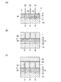
以下に、本発明の実施形態である発光ダイオード及びその製造方法、並びにランプについて、図面を適宜参照しながら説明する。図1は本実施形態の発光ダイオードの断面模式図であり、図2〜図13は発光ダイオードの製造方法を説明する工程図、図14は、本発明の実施形態のダイオードが用いられてなるランプの模式断面図である。尚、以下の説明において参照する図面は、発光ダイオード及びその製造方法を説明する図面であって、図示される各部の大きさや厚さや寸法等は、実際の発光ダイオード等の寸法関係とは異なっている。 Hereinafter, a light-emitting diode, a manufacturing method thereof, and a lamp, which are embodiments of the present invention, will be described with reference to the drawings as appropriate. FIG. 1 is a schematic cross-sectional view of a light-emitting diode according to the present embodiment, FIGS. 2 to 13 are process diagrams illustrating a method for manufacturing the light-emitting diode, and FIG. 14 is a lamp using the diode according to the embodiment of the present invention. FIG. The drawings referred to in the following description are for explaining the light emitting diode and the manufacturing method thereof, and the size, thickness, dimensions, etc. of the respective parts shown in the drawings are different from the dimensional relationships of the actual light emitting diodes, etc. Yes.
[発光ダイオード]
図1に示す例の発光ダイオードAは、基体となるメッキ層1と、メッキ層1上に配置されたシード層2と、シード層2の上に配置された化合物半導体層11と、化合物半導体層11上に配置されたn型電極層9と、から概略構成されている。
[Light emitting diode]
The light-emitting diode A in the example shown in FIG. 1 includes a
ここで、化合物半導体層11は、反射性p型電極層5、p型半導体層6、発光層7及びn型半導体層8が積層されて構成されている。化合物半導体層11の上面は、発光層7からの光を外部に取り出す光取出面11aとされており、この光取出面11a上にはn型電極層9が形成されている。また、光取出面11aはエッチング等の手段によって粗面化されており、これにより発光ダイオードAの光取出効率がより高められている。
Here, the
更に、化合物半導体層11の側面11bと光取り出し面11aの外周部分とには、例えばSiO2等の絶縁性材料からなる保護用の絶縁膜10が形成されている。この絶縁膜10は、反射性p型電極層5及びシード層2の側面まで延在されている。絶縁膜10を形成することによって、例えば化合物半導体層11の側面11bに異物が付着した場合でも、異物によるn型半導体層8とp型半導体層7との短絡が防止される。
Further, a protective insulating
n型電極層9は、化合物半導体層11のn型半導体層8とオーミック接触することによって、化合物半導体層11の負極となっている。図1に示すn型電極層9は、n型半導体層8に接するCr膜9aと、Cr膜9aに積層されたTi膜9bと、Ti膜9bに積層されたAu膜9cとからなる3層構造とされている。n型電極層9はこの3層構造に限らず、Ti膜、Al膜、Ti膜及びAu膜が積層されてなる4層構造でもよい。
このn型電極層9は、後述するように、光取出面11aをプラズマで処理した後にCr膜9a、Ti膜9b及びAu膜9cを順次積層することによって形成され、これによりアニール処理を施すことなくn型半導体層8との間でオーミック接触が得られるようになっている。
The n-
As will be described later, the n-
次に、図1に示すように、化合物半導体層11の下側、つまり、反射性p型電極層5の下側にはシード層2が配置されている。シード層2は、メッキ層1をメッキ法によって形成する際の下地になる層であって、Ti膜2cとTa膜2bとCu膜2aとの積層膜で構成されている。また、シード層2は、Cuからなる単層膜としてもよい。Ti膜2cの厚みは、例えば50〜150nm程度がよく、Ta膜2bの厚みは、例えば200〜400nm程度がよく、Cu膜2aの厚みは、例えば100〜500nm程度がよい。また、シード層2全体の厚みは、例えば350〜1050nm程度がよい。ここでTa膜2bは、Cuのバリアとして機能する。
本実施形態におけるシード層2aの材質は、後述のメッキ層1の材質をCuとした場合には、同じCuを用いることが、密着性が良好となる点から好ましい。
Next, as shown in FIG. 1, the
As the material of the seed layer 2a in the present embodiment, when the material of the later-described
次に、メッキ層1は、シード層2を下地として例えば電気メッキ法により形成される金属層である。メッキ層1の材質は、Cuが好ましい。Cuは、常温でメッキすることが可能であり、成膜時に熱膨張の影響を受け難く、また、電気抵抗が低く熱伝導性が高い点においても上下電極構造の発光ダイオードAの基体の材質として好ましい。メッキ層1の厚みは、例えば300μm程度がよい。メッキ層1を備えることによって、発光ダイオードAの放熱効率が高められる。
Next, the
次に、化合物半導体層11は、反射性p型電極層5とp型半導体層6と発光層7とn型半導体層8とから概略構成されている。
反射性p型電極層5は、シード層2を介してメッキ層1と電気的に接続されており、これによりメッキ層1が反射性p型電極層5の取出電極となっている。また、反射性p型電極層5及びメッキ層1と、n型電極層9とは、化合物半導体層11の厚み方向において反対側に配置された関係になっている。これにより本実施形態の発光ダイオードAは、所謂上下電極構造の発光ダイオードとなっている。
Next, the
The reflective p-
反射性p型電極層5は、p型半導体層6とオーミック接触することによって、化合物半導体層11の正極となっている。
また、反射性p型電極層5は、図1に示すように、化合物半導体層11に接するオーミックコンタクト層5cと、オーミックコンタクト層5cに接する反射層5bと、反射層5bに接する相互拡散防止層5aとから構成されている。反射層5bを備えることによって反射性p型電極層5は、発光層7から発した光を光取出面11a側に反射させる反射層となっている。
この反射性p型電極層5は、後述するように、オーミックコンタクト層5cを、RFスパッタリング法を用いて積層し、反射層5b及び相互拡散防止層5aは例えばDCスパッタリング法を用いて積層することによって形成され、これによりアニール処理を施すことなくp型半導体層6との間でオーミック接触が得られるようになっている。
The reflective p-
As shown in FIG. 1, the reflective p-
As will be described later, the reflective p-
オーミックコンタクト層5cに要求される性能としては、p型半導体層6との接触抵抗が小さいことが必須である。オーミックコンタクト層5cの材料はp型半導体層6との接触抵抗の観点から、Pt、Ru、Os、Rh、Ir、Pd等の白金族またはAgが好ましく、Pt,Ir,RhまたはRuがより好ましく、Ptが特に好ましい。Agを用いることは良好な反射を得るためには好ましいが、接触抵抗はPtよりも高い。したがって、それほど低い接触抵抗が要求されない用途にはAgを用いることも可能である。オーミックコンタクト層5cの厚さは、低接触抵抗を安定して得るために0.1nm以上とすることが好ましい。さらに好ましくは1nm以上であり、均一な接触抵抗が得られる。
As the performance required for the ohmic contact layer 5c, it is essential that the contact resistance with the p-
オーミックコンタクト層5cには、Ag合金、Al合金などの反射層5bが積層されている。Pt,Ir,Rh、Ru、OS,PdなどはAg合金と比較すると可視光から紫外領域の反射率が低い。したがって、発光層7からの光が十分に反射せずに出力の高い素子を得ることが難しい。この場合、オーミックコンタクト層5cを光が十分に透過するほどに薄く形成し、Ag合金などの反射層5bを形成して反射光を得る方が、良好なオーミック接触が得られ、かつ出力の高い素子を作成することができる。この場合、オーミックコンタクト層5cの膜厚は30nm以下とすることが好ましい。さらに好ましくは10nm以下である。反射層5bの膜厚は良好な反射率を得るために0.1nm以上とすることが好ましい。さらに好ましくは1nm以上であり、均一な密着性が得られる。Ag合金はマイグレーションを起こしやすいので薄い方が好ましい。したがって、膜厚は200nm以下にすることが好ましい。
A
相互拡散防止層5aは、反射層5bの構成元素とシード層2の構成元素との相互拡散を防止するために形成される。相互拡散防止層5aとしては、例えば、Pt等を用いることが好ましい。
The
p型半導体層6、発光層7及びn型半導体層8を構成する材料としては、GaN系単結晶、GaP系単結晶、GaAs系単結晶、ZnO系単結晶など周知の半導体発光材料を用いることができるが、後述するサファイア単結晶またはSiC単結晶からなる基板に対してエピタキシャル成長可能な点において、GaN系単結晶またはZnO系単結晶がより好ましく、GaN系単結晶が更に好ましい。
As a material constituting the p-
GaN系単結晶からなる半導体層としては、例えば一般式AlXGaYInZN1−AMA(0≦X≦1、0≦Y≦1、0≦Z≦1で且つ、X+Y+Z=1。記号Mは窒素(N)とは別の第V族元素を表し、0≦A<1である。)で表わされるGaN系半導体が多数知られており、本発明においても、それら周知のGaN系半導体を含めて一般式AlXGaYInZN1−AMA(0≦X≦1、0≦Y≦1、0≦Z≦1で且つ、X+Y+Z=1。記号Mは窒素(N)とは別の第V族元素を表し、0≦A<1である。)で表わされるGaN系半導体を何ら制限なく用いることができる。 As the semiconductor layer made of GaN based single crystal, for example, and by the general formula Al X Ga Y In Z N 1 -A M A (0 ≦ X ≦ 1,0 ≦ Y ≦ 1,0 ≦ Z ≦ 1, X + Y + Z = 1 The symbol M represents a group V element different from nitrogen (N), and 0 ≦ A <1.) There are many known GaN-based semiconductors, and these well-known GaN are also used in the present invention. including system semiconductor and the general formula Al X Ga Y in Z N 1 -a M a (0 ≦ X ≦ 1,0 ≦ Y ≦ 1,0 ≦ Z ≦ 1, X + Y + Z = 1. symbol M nitrogen (N ) Represents another group V element, and 0 ≦ A <1.) A GaN-based semiconductor represented by the above can be used without any limitation.
n型半導体層8は、下地層と、nコンタクト層と、発光層7に接するnクラッド層とが積層されて構成される。nコンタクト層は下地層および/またはnクラッド層を兼ねることができる。
下地層はAlXGa1―XN層(0≦x≦1、好ましくは0≦x≦0.5、さらに好ましくは0≦x≦0.1)から構成されることが好ましい。その膜厚は0.1μm以上、好ましくは0.5μm以上、さらに好ましくは1μm以上である。この膜厚以上にした方が結晶性の良好なAlXGa1―XN層が得られやすい。
下地層にはn型不純物を1×10¹⁷〜1×10¹⁹/cm3の範囲内であればドープしても良いが、アンドープ(<1×1017/cm3)の方が良好な結晶性の維持という点で好ましい。n型不純物としては、特に限定されないが、例えば、Si、GeおよびSn等が挙げられ、好ましくはSiおよびGeであり、より好ましくはSiである。
The n-
Underlayer Al X Ga 1-X N layer (0 ≦ x ≦ 1, preferably 0 ≦ x ≦ 0.5, and more preferably 0 ≦ x ≦ 0.1) is preferably configured from. The film thickness is 0.1 μm or more, preferably 0.5 μm or more, more preferably 1 μm or more. An Al X Ga 1-X N layer with good crystallinity is more easily obtained when the thickness is increased.
The underlayer may be doped with n-type impurities within the range of 1 × 10 17 to 1 × 10 19 / cm 3 , but undoped (<1 × 10 17 / cm 3 ) is a better crystal. It is preferable in terms of maintaining the property. Although it does not specifically limit as an n-type impurity, For example, Si, Ge, Sn, etc. are mentioned, Preferably it is Si and Ge, More preferably, it is Si.
nコンタクト層としては、下地層と同様にAlXGa1―XN層(0≦x≦1、好ましくは0≦x≦0.5、さらに好ましくは0≦x≦0.1)から構成されることが好ましい。また、nコンタクト層にはn型不純物がドープされていることが好ましく、n型不純物を1×10¹⁷〜1×10¹⁹/cm3、好ましくは1×1018〜1×1019/cm3の濃度で含有すると、n型電極層9との良好なオーミック接触の維持、クラック発生の抑制、良好な結晶性の維持の点で好ましい。n型不純物としては、特に限定されないが、例えば、Si、GeおよびSn等が挙げられ、好ましくはSiおよびGeであり、より好ましくはSiである。
nコンタクト層を構成するGaN系半導体は、下地層と同一組成であることが好ましく、nコンタクト層と下地層との合計の膜厚を1〜20μm、好ましくは2〜15μm、さらに好ましくは3〜12μmの範囲に設定することが好ましい。nコンタクト層と下地層との合計の膜厚が上記範囲にあると、半導体の結晶性が良好に維持される。
The n-contact layer, as an underlying layer Al X Ga 1-X N layer (0 ≦ x ≦ 1, preferably 0 ≦ x ≦ 0.5, and more preferably 0 ≦ x ≦ 0.1) is composed of It is preferable. The n contact layer is preferably doped with an n-type impurity, and the n-type impurity is preferably 1 × 10 17 to 1 × 10 19 / cm 3 , preferably 1 × 10 18 to 1 × 10 19 / cm 3. If it is contained at a concentration of 1, it is preferable in terms of maintaining good ohmic contact with the n-
The GaN-based semiconductor constituting the n contact layer preferably has the same composition as that of the base layer, and the total film thickness of the n contact layer and the base layer is 1 to 20 μm, preferably 2 to 15 μm, more preferably 3 to 3. It is preferable to set in the range of 12 μm. When the total film thickness of the n-contact layer and the underlayer is in the above range, the crystallinity of the semiconductor is favorably maintained.
nコンタクト層と発光層7との間には、nクラッド層を設けることが好ましい。nコンタクト層の表面に生じた平坦性の悪化を埋めることできるからである。nクラッド層はAlGaN、GaN、GaInNなどで形成することが可能である。また、これらの構造のヘテロ接合や複数回積層した超格子構造としてもよい。nクラッド層をGaInNで形成する場合には、発光層7のGaInNのバンドギャップよりも大きくすることが望ましいことは言うまでもない。
nクラッド層の膜厚は、特に限定されないが、好ましくは0.005〜0.5μmであり、より好ましくは0.005〜0.1μmである。nクラッド層のn型ドーパント濃度は1×10¹⁷〜1×10²⁰/cm3が好ましく、より好ましくは1×1018〜1×1019/cm3である。ドーパント濃度がこの範囲であると、良好な結晶性の維持および素子の動作電圧低減の点で好ましい。
It is preferable to provide an n clad layer between the n contact layer and the
The thickness of the n-clad layer is not particularly limited, but is preferably 0.005 to 0.5 μm, more preferably 0.005 to 0.1 μm. The n-type dopant concentration of the n-clad layer is preferably 1 × 10 17 to 1 × 10 20 / cm 3 , more preferably 1 × 10 18 to 1 × 10 19 / cm 3 . A dopant concentration within this range is preferable in terms of maintaining good crystallinity and reducing the operating voltage of the device.
次に、n型半導体層8の下側に積層される発光層7としては、GaN系半導体、好ましくはGa1−sInsN(0<s<0.4)のGaN系半導体からなる発光層が本発明では通常用いられる。発光層7の膜厚としては、特に限定されないが、量子効果の得られる程度の膜厚、即ち臨界膜厚が挙げられ、例えば好ましくは1〜10nmであり、より好ましくは2〜6nmである。発光層7の膜厚が上記範囲であると発光出力の点で好ましい。
また、発光層7は、上記のような単一量子井戸(SQW)構造の他に、上記Ga1−sInsNを井戸層として、この井戸層よりバンドギャップエネルギーが大きいAlcGa1−cN(0≦c<0.3)障壁層とからなる多重量子井戸(MQW)構造としてもよい。また、井戸層および障壁層には、不純物をドープしてもよい。
Next, as the
In addition to the single quantum well (SQW) structure as described above, the
次に、p型半導体層6は、発光層7に接するpクラッド層と、pコンタクト層とが積層されて構成される。しかし、pコンタクト層がpクラッド層を兼ねてもよい。
pクラッド層としては、発光層7のバンドギャップエネルギーより大きくなる組成であり、発光層7へのキャリアの閉じ込めができるものであれば特に限定されないが、好ましくは、AldGa1−dN(0<d≦0.4、好ましくは0.1≦d≦0.3)のものが挙げられる。pクラッド層が、このようなAlGaNからなると、発光層7へのキャリアの閉じ込めの点で好ましい。pクラッド層の膜厚は、特に限定されないが、好ましくは1〜400nmであり、より好ましくは5〜100nmである。pクラッド層のp型ドーパント濃度は、1×10¹⁸〜1×10²¹/cm3が好ましく、より好ましくは1×1019〜1×1020/cm3である。p型ドーパント濃度が上記範囲であると、結晶性を低下させることなく良好なp型結晶が得られる。
Next, the p-
The p-cladding layer is not particularly limited as long as it has a composition larger than the band gap energy of the light-emitting
pコンタクト層は、少なくともAleGa1−eN(0≦e<0.5、好ましくは0≦e≦0.2、より好ましくは0≦e≦0.1)を含んでなるGaN系半導体層である。Al組成が上記範囲であると、良好な結晶性の維持および反射性p型電極層5との良好なオーミック接触の点で好ましい。p型不純物(ドーパント)を1×10¹⁸〜1×10²¹/cm3の濃度で、好ましくは5×1019〜5×1020/cm3の濃度で含有していると、良好なオーミック接触の維持、クラック発生の防止、良好な結晶性の維持の点で好ましい。p型不純物としては、特に限定されないが、例えば好ましくはMgが挙げられる。膜厚は、特に限定されないが、0.01〜0.5μmが好ましく、より好ましくは0.05〜0.2μmである。膜厚がこの範囲であると、発光出力の点で好ましい。
The p-contact layer comprises at least Al e Ga 1-e N (0 ≦ e <0.5, preferably 0 ≦ e ≦ 0.2, more preferably 0 ≦ e ≦ 0.1). Is a layer. When the Al composition is within the above range, it is preferable in terms of maintaining good crystallinity and good ohmic contact with the reflective p-
[発光ダイオードの製造方法]
次に、図2〜図14を参照して、発光ダイオードAの製造方法について説明する。本実施形態の発光ダイオードAの製造方法は、基板21上に複数の化合物半導体層11を形成する積層工程と、複数の化合物半導体層11の各々の間の分離溝12に平坦化用レジスト層23を埋め込むように形成する平坦化工程と、複数の化合物半導体層11及び平坦化用レジスト層23の上にシード層2を形成するシード層形成工程と、シード層2上に、平坦化用レジスト層23に沿う分離用レジスト層22を包含し、該分離用レジスト層22によって一部が分断されてなるメッキ層1を形成するとともに、該メッキ層1に仮貼付基板24を貼り付けるメッキ工程と、基板21を複数の化合物半導体層11及び平坦化用レジスト層23から剥離して、複数の化合物半導体層11に備えられるn型半導体層8の光取出面11aを露出させるとともに、平坦化用レジスト層23及び分離用レジスト層22を除去する除去工程と、複数の化合物半導体層11に備えられるn型半導体層8上にn型電極層9を形成する電極形成工程と、仮貼付基板24を除去する仮貼付基板除去工程と、メッキ層1の内、分離用レジスト層22によって分断された部分に沿って、メッキ層1を切断するダイシング工程と、から概略構成されている。
また、本実施形態で説明する例では、前記除去工程と前記電極形成工程との間において、複数の化合物半導体層11の各側面(周囲面)11bに、保護用の絶縁膜10を形成する絶縁膜形成工程が設けられている。またさらに、本例では、前記絶縁膜形成工程と前記電極形成工程との間において、n型半導体層8の光取出面11aを粗面化する粗面化工程が設けられている。
[Method for manufacturing light-emitting diode]
Next, with reference to FIGS. 2-14, the manufacturing method of the light emitting diode A is demonstrated. In the method of manufacturing the light emitting diode A according to the present embodiment, a stacking process for forming the plurality of compound semiconductor layers 11 on the
In the example described in this embodiment, the insulating
『製造方法の一例』
以下、本実施形態の発光ダイオードの製造方法の一例について、図面を参照しつつ各工程を説明する。
"Example of manufacturing method"
Hereafter, each process is demonstrated, referring drawings for an example of the manufacturing method of the light emitting diode of this embodiment.
「積層工程」
積層工程では、図2(a)〜図2(c)に示すように、基板21上に、n型半導体層8、発光層7、p型半導体層6及び反射性p型電極層5を順次積層して複数の化合物半導体層11を形成する。
"Lamination process"
In the laminating step, as shown in FIGS. 2A to 2C, the n-
具体的には、まず、図2(a)に示すように、基板21上に、n型半導体層8、発光層7及びp型半導体層6を順次積層する。
n型半導体層8にはn型ドーパントとしてSi等をドープさせることが望ましく、p型半導体層6にはp型ドーパントとしてMg等をドープさせることが望ましい。
また、基板21上に化合物半導体層11を構成するn型半導体層8、発光層7及びp型半導体層6の各々を形成する際には、あらかじめ基板21上にバッファ層を形成することが望ましい。すなわち、基板21としてサファイア基板を用い、n型半導体層8としてGaNを形成する場合には、基板21とn型半導体層8との格子定数が10%以上も異なる。この場合に、バッファ層として、基板21とn型半導体層8との中間の格子定数を有するAlNやAlGaNなどを用いることで、n型半導体層8を構成するGaNの結晶性を向上させることができる。
Specifically, first, as shown in FIG. 2A, the n-
The n-
In addition, when each of the n-
この際、化合物半導体層11を構成するn型半導体層8、発光層7及びp型半導体層6の成長方法は特に限定されず、スパッタリング法、MOCVD(有機金属化学気相成長法)、HVPE(ハイドライド気相成長法)、MBE(分子線エピタキシー法)、などGaN系半導体を成長させることが知られている全ての方法を適用できる。好ましい成長方法としては、膜厚制御性、量産性の観点からスパッタリング法またはMOCVD法である。
At this time, the growth method of the n-
スパッタリング法では、Gaを含むターゲットを用いるとともに、プラズマガスとしてアルゴンと窒素の混合ガスを用いて、所謂リアクティブスパッタリング法によってGaN系半導体を形成することが好ましい。
また、MOCVD法では、キャリアガスとして水素(H2)または窒素(N2)、III族原料であるGa源としてトリメチルガリウム(TMG)またはトリエチルガリウム(TEG)、Al源としてトリメチルアルミニウム(TMA)またはトリエチルアルミニウム(TEA)、In源としてトリメチルインジウム(TMI)またはトリエチルインジウム(TEI)、V族原料であるN源としてアンモニア(NH3)、ヒドラジン(N2H4)などが用いられる。また、ドーパントとしては、n型にはSi原料としてモノシラン(SiH4)またはジシラン(Si2H6)を、Ge原料としてゲルマンガス(GeH4)や、テトラメチルゲルマニウム((CH3)4Ge)やテトラエチルゲルマニウム((C2H5)4Ge)等の有機ゲルマニウム化合物を利用できる。
MBE法では、元素状のゲルマニウムもドーピング源として利用できる。p型にはMg原料としては例えばビスシクロペンタジエニルマグネシウム(Cp2Mg)またはビスエチルシクロペンタジエニルマグネシウム(EtCp2Mg)を用いればよい。
In the sputtering method, it is preferable to form a GaN-based semiconductor by a so-called reactive sputtering method using a target containing Ga and using a mixed gas of argon and nitrogen as a plasma gas.
In the MOCVD method, hydrogen (H 2 ) or nitrogen (N 2 ) as a carrier gas, trimethyl gallium (TMG) or triethyl gallium (TEG) as a Ga source which is a group III source, trimethyl aluminum (TMA) or Al as a source Triethylaluminum (TEA), trimethylindium (TMI) or triethylindium (TEI) as an In source, ammonia (NH 3 ), hydrazine (N 2 H 4 ), or the like as an N source as a group V raw material are used. In addition, as a dopant, for n-type, monosilane (SiH 4 ) or disilane (Si 2 H 6 ) is used as a Si raw material, germanium gas (GeH 4 ) or tetramethyl germanium ((CH 3 ) 4 Ge) is used as a Ge raw material. And organic germanium compounds such as tetraethylgermanium ((C 2 H 5 ) 4 Ge) can be used.
In the MBE method, elemental germanium can also be used as a doping source. For the p-type, for example, biscyclopentadienyl magnesium (Cp 2 Mg) or bisethylcyclopentadienyl magnesium (EtCp 2 Mg) may be used as the Mg raw material.
次に、図2(b)に示すように、上記手順にて基板21上に順次積層されたn型半導体層8、発光層7及びp型半導体層6を、複数の積層体として分割し、分割溝12を形成する。
Next, as shown in FIG. 2B, the n-
具体的には、図2(b)に示すように、化合物半導体層11を構成するp型半導体層6上にマスクを形成し、ドライエッチング等の手段によってp型半導体層6、発光層7及びn型半導体層8からなる積層体を格子状にエッチングして分割する。エッチングによる処理は、基板21が露出した時点で終了する。これにより、p型半導体層6、発光層7及びn型半導体層8からなる積層体を、分割溝12に沿って複数に分割された積層体とする。
Specifically, as shown in FIG. 2B, a mask is formed on the p-
次に、図2(c)に示すように、p型半導体層6上に、フォトリソグラフィ技術によって、オーミックコンタクト層、反射層及び相互拡散防止層を順次積層し、パターニングすることにより、反射性p型電極層5を形成する。
Next, as shown in FIG. 2C, an ohmic contact layer, a reflective layer, and an interdiffusion prevention layer are sequentially stacked on the p-
オーミックコンタクト層をp型半導体層6上に形成するにあたり、RF放電によるスパッタリング成膜法で形成することが好ましい。RF放電によるスパッタリング成膜法を用いることで、蒸着法やDC放電のスパッタリング成膜法を用いるより接触抵抗の低い電極を形成できる。即ち、RF放電によるスパッタリング成膜法でオーミックコンタクト層を形成することによって、オーミックコンタクト層にp型半導体層6の構成元素が混在し、p型半導体層6にはオーミックコンタクト層の構成元素が混在することになり、これによりオーミックコンタクト層とp型半導体層6とがオーミック接合される。
In forming the ohmic contact layer on the p-
RF放電によるスパッタリング成膜では、イオンアシスト効果により、p型半導体層6に付着したスパッタ原子にエネルギーを与え、p型半導体、例えばMgドープのp−GaNとの間で表面拡散を促す作用があると考えられる。さらに、上記成膜においては、p型半導体層6の最表面原子にもエネルギーを与え、半導体材料、例えばGaがオーミックコンタクト層に拡散することを促す作用もあると考えられる。
In sputtering film formation by RF discharge, energy is given to sputtered atoms attached to the p-
RF放電による成膜では、初期において、接触抵抗を下げる効果を持つが、膜厚を大きくすると、その膜が疎であるために反射率の点ではDC放電による成膜に比べて劣る。そこで、接触抵抗を低く保った範囲で薄膜化して光透過率を上げたオーミックコンタクト層をRF放電により形成し、その上に反射層及び相互拡散防止層をDC放電により形成することが好ましい。 The film formation by RF discharge has an effect of lowering the contact resistance in the initial stage. However, when the film thickness is increased, the film is sparse, so that the reflectivity is inferior to the film formation by DC discharge. Therefore, it is preferable to form an ohmic contact layer that is thinned and increases the light transmittance within a range in which contact resistance is kept low by RF discharge, and a reflective layer and an interdiffusion prevention layer are formed thereon by DC discharge.
上記の如く、オーミックコンタクト層をRFスパッタリング法により形成することによって、オーミックコンタクト層とp型半導体層6とをオーミック接触させることができる。この場合、オーミックコンタクト層形成後のアニールを必要としない。むしろ、アニールすることにより、Pt、Gaそれぞれの拡散を促進し、半導体の結晶性を下げてしまうため、電気特性を悪化させてしまうことがあり、また、反射膜のAg合金がマイグレーションを起こし、反射率が低下するので好ましくない。従ってオーミックコンタクト層形成後、350℃よりも高い温度で熱処理されていないことが好ましい。
As described above, the ohmic contact layer and the p-
スパッタリングは、従来公知のスパッタリング装置を用いて従来公知の条件を適宜選択して実施することができる。化合物半導体層11を積層した基板21をチャンバ内に収容し、基板温度を室温から500℃の範囲に設定する。基板加熱は特に必要としないが、オーミックコンタクト層の構成元素およびp型半導体層6の構成元素の拡散を促進するために適度に加熱しても良い。チャンバ内は真空度が10−4〜10−7Paとなるまで排気する。スパッタリング用ガスとしては、He、Ne、Ar、Kr、Xe等が使用できる。入手の容易さからArとするのが望ましい。これらの内の一つのガスをチャンバ内に導入し、0.1〜10Paにしたのち放電を行う。好ましくは0.2〜5Paの範囲に設定する。供給する電力は0.2〜2.0kWの範囲が好ましい。この際、放電時間と供給電力を調節することによって、形成する層の厚さを調節することができる。
Sputtering can be carried out by appropriately selecting conventionally known conditions using a conventionally known sputtering apparatus. The
「平坦化工程」
次に、平坦化工程では、図3に示すように、基板21上において、複数の化合物半導体層11の各々の間の分離溝12に、平坦化用レジスト層23を埋め込むように形成する。
"Planarization process"
Next, in the planarization step, as shown in FIG. 3, the planarization resist
具体的には、図3に示すように、複数の化合物半導体層11の各々の間に形成された分離溝12に平坦化用レジスト層23を埋め込み、平面視で略格子状に形成する。平坦化用レジスト層23としては、従来公知のレジスト材料を用いることができる。
Specifically, as shown in FIG. 3, a planarization resist
「シード層形成工程」
次に、シード層形成工程では、図4に示すように、複数の化合物半導体層11及び平坦化用レジスト層23の上にシード層2を形成する。
"Seed layer formation process"
Next, in the seed layer forming step, as shown in FIG. 4, the
具体的には、図4に示すように、複数の化合物半導体層11に備えられる反射性p型電極層5と平坦化用レジスト層23を覆うように、Ti膜2cとTa膜2bとCu膜2aとを順次積層してシード層2を形成する。なお、シード層は、Ni膜とAu膜とTi膜とTa膜とCu膜とを順次積層して形成しても良い。
Specifically, as shown in FIG. 4, a
「メッキ工程」
次に、メッキ工程では、図5(a)〜図5(c)に示すように、シード層2上に、平坦化用レジスト層23に沿う分離用レジスト層22を包含し、該分離用レジスト層22によって一部が分断されてなるメッキ層1を形成するとともに、該メッキ層1に仮貼付基板24を貼り付ける。
"Plating process"
Next, in the plating step, as shown in FIGS. 5A to 5C, a separation resist
具体的には、まず、図5(a)に示すように、シード層2上において、平坦化用レジスト層23に沿うようにして、分離用レジスト層22を平面視略格子状に形成する。このような分離用レジスト層22としては、従来公知のレジスト材料を用い、例えば、高さ寸法が150〜300μm程度、幅が数十μm程度になるように形成すればよい。
次に、図5(b)に示すように、シード層2及び分離用レジスト層22を覆うようにメッキ層1を形成する。メッキ層1の形成は、シード層2に電流を印加しつつ電気メッキ法で行うとよい。この際、メッキ層1の厚みを、200〜350μm程度として分離用レジスト層22の高さよりも厚く形成することにより、図示するような、分離用レジスト層22によって一部が分断されてなるメッキ層1を形成することができる。
そして、図5(c)に示すように、メッキ層1に仮貼付基板24を、熱発泡テープ25を用いて貼り付ける。
Specifically, first, as shown in FIG. 5A, on the
Next, as shown in FIG. 5B, the
Then, as shown in FIG. 5C, the
「除去工程」
次に、除去工程では、図6(a)〜図6(c)に示すように、基板21及び図示略のバッファ層を、複数の化合物半導体層11及び前記平坦化用レジスト層23から剥離して、複数の化合物半導体層11に備えられるn型半導体層8の光取出面11aを露出させるとともに、平坦化用レジスト層23及び分離用レジスト層22を除去する。
図示略のバッファ層及び基板21を取り除く方法としては、研磨法、エッチング法、レーザリフトオフ法など公知の技術を何ら制限なく用いることが出来るが、本例では生産性の観点からレーザリフトオフ法を用いることが好ましい。
また、平坦化用レジスト層23及び分離用レジスト層22の除去には、溶剤(NMP等)のジェット噴霧による方法を用いることが好ましい。
"Removal process"
Next, in the removing step, as shown in FIGS. 6A to 6C, the
As a method for removing the buffer layer and the substrate 21 (not shown), a known technique such as a polishing method, an etching method, or a laser lift-off method can be used without any limitation. In this example, the laser lift-off method is used from the viewpoint of productivity. It is preferable.
Further, it is preferable to use a method of jetting a solvent (NMP or the like) for removing the planarizing resist
具体的には、まず、図6(a)に示すように、バッファ層と基板21との界面近傍にレーザ光Lを照射し、主にバッファ層を熱分解させることによって、図6(b)に示すようにn型半導体層8及び平坦化用レジスト層23から基板21を剥離させる。n型半導体層8及び平坦化用レジスト層23から基板21及びバッファ層を取り除くことによって、n型半導体層8のバッファ層との接合面及び平坦化用レジスト層23が露出される。
次に、図6(c)に示すように、複数の化合物半導体層11の各々の間に埋め込まれた平坦化用レジスト層23と、分離用レジスト層22の上のシード層2と、分離用レジスト層22を、溶剤(NMP等)のジェット噴霧によって一度に除去する。また、メッキ層1において分離用レジスト層22によって分断された部分には、分断溝1bが形成される。この際、メッキ層1の厚さ及び分離用レジスト層22の高さを上記範囲とし、メッキ層1における分断溝1bの底部で残存した部分を、例えば、50〜60μm程度とすることにより、後述のダイシング工程において、レーザスクライブを用いた切断が容易になる。
Specifically, first, as shown in FIG. 6A, the vicinity of the interface between the buffer layer and the
Next, as shown in FIG. 6C, the planarization resist
「絶縁膜形成工程」
次に、絶縁膜形成工程では、図7に示すように、複数に分割された化合物半導体層11の各側面(周囲面)11bに、保護用の絶縁膜10を形成する。
具体的には、図7に示すように、CVD法やスパッタ法等の手段によって、SiO2からなる絶縁膜10を、各化合物半導体層11の側面11bと、各化合物半導体層11の光取り出し面11aの外周部分を覆うように形成する。化合物半導体層11の全体に絶縁膜10を形成し、光取出面11aの中央部以外の部分にレジストを形成し、ドライエッチングすることで、目的の絶縁膜10を形成できる。
"Insulating film formation process"
Next, in the insulating film forming step, as shown in FIG. 7, a protective insulating
Specifically, as shown in FIG. 7, the insulating
「粗面化工程」
次に、粗面化工程では、n型半導体層8の光取出面11aを粗面化する。
具体的には、詳細な図示を省略するが、加熱KOH溶液に浸漬して、光取出面11aの中央の絶縁膜10に被覆されずに露出している部分の、n型半導体層8を構成する図示略の下地層を除去するとともに、n型半導体層8の光取出面11aを粗面化する。
下地層の除去及び粗面化には、PEC(photo electrochemical etch)を使用することもできる。また、下地層の除去及び光取出面11aの粗面化にはドライエッチングを適用することもできる。
尚、上記の下地層の除去操作は、下地層がアンドープ層である場合に必要な操作であって、下地層にSi等がドープされている場合には下地層の除去操作は不要である。
"Roughening process"
Next, in the roughening step, the
Specifically, although not shown in detail, the n-
PEC (photoelectrochemical etch) can also be used for the removal of the underlayer and the roughening. Also, dry etching can be applied to the removal of the underlayer and the roughening of the
The above-described underlayer removal operation is necessary when the underlayer is an undoped layer, and when the underlayer is doped with Si or the like, the underlayer removal operation is not necessary.
「電極形成工程」
電極形成工程では、図8に示すように、n型半導体層8の光取出面11aを、n型半導体層8中のドーパント元素と同一の元素を含有するエッチングガスによりドライエッチングしてから、光取出面11aにn型電極層9を形成する。
具体的には、メッキ層1及び化合物半導体層11等を含むメッキ基板をプラズマドライエッチング装置のチャンバに収納し、n型半導体層8中のドーパント元素と同一の元素を含有するエッチングガスからなる反応ガスをチャンバ内に供給し、化合物半導体層11の上方においてプラズマを発生させ、エッチングガスを含むプラズマを光取出面11aに暴露させる。
"Electrode formation process"
In the electrode forming step, as shown in FIG. 8, the
More specifically, a plating substrate including the
エッチングガスとしては、n型半導体層8中のドーパント元素がケイ素(Si)の場合は、エッチングガスとしてハロゲン化ケイ素を用いることが好ましく、具体的にはSiCl4またはSiF4が好ましい。
また、反応ガスを導入した際のチャンバ内の圧力は、例えば0.2〜2Paの範囲にすることが好ましく、エッチングガスの流量は15sccm〜50sccmの範囲が好ましく、プラズマのパワーは120W程度が好ましく、バイアスは50W程度が好ましく、処理時間は150秒程度がよい。
このようなエッチング処理を行うことによって、n型半導体層8の表面近傍にエッチングガスに含まれるSiが打ち込まれて、表面近傍のSi濃度が高められると考えられる。
As the etching gas, when the dopant element in the n-
The pressure in the chamber when the reaction gas is introduced is preferably in the range of 0.2 to 2 Pa, the flow rate of the etching gas is preferably in the range of 15 sccm to 50 sccm, and the plasma power is preferably about 120 W. The bias is preferably about 50 W, and the processing time is preferably about 150 seconds.
By performing such an etching process, it is considered that Si contained in the etching gas is implanted in the vicinity of the surface of the n-
次に、図8に示すように、プラズマ処理後のn型半導体層8の上に、Cr膜、Ti膜及びAu膜を順次積層してn型電極層9を形成する。また、n型電極層9は、このような3層構造に限らず、Ti膜、Al膜、Ti膜及びAu膜が積層されてなる4層構造でもよい。n型電極層9の形成は、例えば、スパッタリング法や蒸着法を用いればよい。
上記の如く、n型半導体層8の表面をプラズマで処理してから、Cr膜またはTi膜等を積層することによって、n型電極層9を構成するCr膜またはTi膜とn型半導体層8とをオーミック接触させることができる。この場合、n型電極層9の形成後のアニールを必要としない。むしろ、アニールすることによって電気特性を悪化させてしまうことがあり、また、反射膜のAg合金がマイグレーションを起こし、反射率が低下するので好ましくない。
Next, as shown in FIG. 8, an n-
As described above, after the surface of the n-
「仮貼付基板除去工程」
次に、仮貼付基板除去工程では、図9に示すように、仮貼付基板24をメッキ層1から剥離、除去する。
具体的には、図9に示すように、メッキ層1に仮貼付基板24を貼着している熱発泡テープ25を加熱することで貼着力を低下させることにより、仮貼付基板24をメッキ層1から引き剥がして除去する。
"Temporary stuck substrate removal process"
Next, in the temporary sticking substrate removing step, the
Specifically, as shown in FIG. 9, the
「ダイシング工程」
次に、ダイシング工程では、図10〜図11に示すように、メッキ層1の内、分離用レジスト層22(図6(b)等参照)によって分断された部分に沿って、メッキ層1を切断する。
具体的には、図10に示すように、メッキ層1において、前記除去工程において分離用レジスト層22が除去されることによって形成された分断溝1bの底部で残存した部分に沿って、例えば、レーザスクライブ法を用いてレーザを照射して切断する。この際、メッキ層1における分断溝1b底部の残存部分が60μm以下であれば、この部分をレーザ照射によって容易に切断することができる。また、この際、メッキ層1のレーザによる切断面は、メッキ層1を構成する銅が溶融した状態となる。
その後、上記方法で切断された分断溝1bの底部は、各々の切断面同士が溶融銅によって再溶着する。
これにより、メッキ層1全体が再溶着された状態となるため、分断された素子が飛び散ること無くウェーハ全体で保持される。一方、上記のように再溶着した銅は強度面で脆いので、微弱な機械的応力を印加することにより、容易にブレークして切断、分割することができ、複数のダイオードAが得られる。
このようなダイシング工程を行なうことにより、図11(図1も参照)に示すような、複数の発光ダイオードAが得られる。
"Dicing process"
Next, in the dicing process, as shown in FIGS. 10 to 11, the
Specifically, as shown in FIG. 10, in the
Thereafter, the cut surfaces of the dividing
As a result, since the
By performing such a dicing process, a plurality of light emitting diodes A as shown in FIG. 11 (see also FIG. 1) can be obtained.
なお、ダイシング工程においてメッキ層1を切断し、複数のダイオードAを得る方法としては、上記したレーザスクライブ法の他、例えば、メッキ層1の化合物半導体層11と反対側の面1aを、CMP(Chemical Mechanical Polishing)等の方法で研磨することにより、メッキ層1における分断溝1bの底部で残存した部分を除去する方法を用いることも可能である。
In addition, as a method of cutting the
『製造方法の他の例』
以下、本発明の発光ダイオードの製造方法の他の例について、図面を参照しつつ各工程を説明する。なお、本例においては、上述したような本実施形態の製造方法の一例と共通する構成については共通の符号を付与するとともに共通の図面を用いて説明し、また、各例において共通する工程については、図面やその詳しい説明を省略する。
“Other examples of manufacturing methods”
Hereafter, each process is demonstrated, referring drawings for the other example of the manufacturing method of the light emitting diode of this invention. In addition, in this example, about the structure which is common with an example of the manufacturing method of this embodiment as mentioned above, it attaches | subjects a common code | symbol and demonstrates using a common drawing, Moreover, about the process which is common in each example The drawings and detailed description thereof are omitted.
本例の発光ダイオードの製造方法では、主として、メッキ工程において、シード層2上に第1メッキ層16を形成した後、該第1メッキ層16上に分離用レジスト層22を形成するとともに、該分離用レジスト層22と同じ厚さ寸法の第2メッキ層17を形成することにより、分離用レジスト層22によって一部が分断されてなるメッキ層15を形成する方法とした点で、上述したような本実施形態の製造方法の一例とは異なる。
また、本例では、積層工程及びシード層形成工程については、上記製造方法の一例と共通であるので、上記したメッキ工程以降の工程を中心に説明する。
In the light emitting diode manufacturing method of this example, mainly in the plating process, after forming the
Further, in this example, the lamination process and the seed layer forming process are common with the above-described manufacturing method, and therefore, description will be made mainly on the processes after the plating process.
本例のメッキ工程では、まず、図12(a)に示すように、シード層2上に、第1メッキ層16を形成する。この際、第1メッキ層16の厚さを、例えば、60μmとして形成する。
次に、図12(b)に示すように、第1メッキ層16上に、分離用レジスト層22を形成する。この際、分離用レジスト層22を、例えば、高さ寸法が100〜250μm程度、幅が数十μm程度になるように形成する。
次に、図12(c)に示すように、第1メッキ層16及び分離用レジスト層22を覆うように第2メッキ層17を形成することにより、分離用レジスト層22を包含するメッキ層15を形成する。このような各メッキ層の形成処理は、上記製造方法の一例と同様、シード層2に電流を印加しつつ電気メッキ法で行うことができる。
そして、図12(d)に示すように、メッキ層1に仮貼付基板24を、熱発泡テープ25を用いて貼り付ける。
In the plating process of this example, first, a
Next, as shown in FIG. 12B, a separation resist
Next, as shown in FIG. 12C, the
Then, as shown in FIG. 12 (d), a
本例では、メッキ層15を上記方法で形成することにより、図12(c)及び図12(d)に示すような、分離用レジスト層22によって一部が分断されてなるメッキ層15となる。このメッキ層15は、後述の除去工程における分離用レジスト22の除去によって分断溝15b(図13(c)参照)が形成され、この分断溝15bの底部に残存する部分が化合物半導体層11側に配されている点で、図5(c)に示す一例のメッキ層1とは異なる。
In this example, by forming the
次に、本例の除去工程では、まず、図13(a)及び図13(b)に示すように、上記製造方法の一例と同様の方法を用いて、基板21を、複数の化合物半導体層11及び平坦化用レジスト層23から剥離して、複数の化合物半導体層11に備えられるn型半導体層8の光取出面11aを露出させる。
次に、図13(c)に示すように、平坦化用レジスト層23及び分離用レジスト層22を、溶解除去もしくはアッシング除去の何れかの方法を用いて除去する。また、この際、メッキ層15に包含される分離用レジスト層22の除去は、仮貼付基板24を一時剥離して行なう。この際、メッキ層15において分離用レジスト層22によって分断された部分には、分断溝15bが形成される。このようにして、平坦化用レジスト層23及び分離用レジスト層22を除去した後、図13(d)に示すように、再度、メッキ層15に仮貼付基板24を貼り付ける。
Next, in the removal step of this example, first, as shown in FIGS. 13A and 13B, the
Next, as shown in FIG. 13C, the planarization resist
次に、本例では、絶縁膜形成工程、粗面化工程、電極形成工程、仮貼付基板除去工程及びダイシング工程については、上記した製造方法の一例と同様の方法を用いることができる。本例では、上記した各工程により、図11(図1も参照)に示すような、複数の発光ダイオードAが得られる。 Next, in this example, the same method as the above-described manufacturing method can be used for the insulating film forming step, the roughening step, the electrode forming step, the temporary sticking substrate removing step, and the dicing step. In this example, a plurality of light emitting diodes A as shown in FIG. 11 (see also FIG. 1) are obtained by the above-described steps.
以上説明したように、本実施形態の発光ダイオードAの製造方法によれば、上記構成の如く、メッキ層1に仮貼付基板24を貼り付けることにより、サファイアからなる基板21を除去した後のウェーハに剛性を持たせることができるので、取り扱い性を向上させることが可能となる。
また、メッキ層1において、分離用レジスト層22の除去によって形成される分断溝1bの底部の残存部分に沿って、レーザスクライブによってメッキ層1を切断するダイシング工程が備えられているので、メッキ層1のレーザによる切断面が溶融状態となった後、各々の切断面同士が溶融銅によって再溶着し、分断された素子が飛び散ること無くウェーハ全体で保持される。一方、再溶着した銅は脆いので、容易にブレークして切断、分割することができ、また、ダイシング用のテーブル上に粘着テープを貼り付け、この上にウェーハを設置することにより、再溶着した複数の素子を容易に分割して複数のダイオードAとして取り出すことができるので、素子分割時の管理を容易になる。従って、素子特性に優れた発光ダイオードAを高効率で製造することが可能となる。
As described above, according to the method for manufacturing the light-emitting diode A of the present embodiment, the wafer after the
Further, the
また、本実施形態の発光ダイオードAの製造方法によれば、化合物半導体層11にメッキ層1を形成し、その後、基板21を除去することによって、n型電極層9及びメッキ層1によって化合物半導体層11が挟まれた所謂上下電極構造の発光ダイオードAを形成することができる。このようにして得られた発光ダイオードAは、Cu等からなるメッキ層1を備えるので、発光に伴って発生した熱を容易に放熱させることができる。
Further, according to the method for manufacturing the light emitting diode A of the present embodiment, the
また、上記の発光ダイオードAの製造方法によれば、シード層2を形成し、シード層2にメッキ層1を形成するので、シード層2を介してメッキ層1を強固に接合させることができ、機械的強度に優れた発光ダイオードAを製造できる。
Moreover, according to the manufacturing method of the light emitting diode A, the
[ランプ]
以上説明したような、本発明に係る発光ダイオードの製造方法によって得られる、図1に示すような上下電極型の発光ダイオードAと蛍光体とを組み合わせることにより、当業者周知の手段を用いてランプを構成することができる。従来より、発光素子と蛍光体と組み合わせることによって発光色を変える技術が知られており、本発明では、このような技術を何ら制限されることなく採用することが可能である。
例えば、蛍光体を適正に選定することにより、発光素子より長波長の発光を得ることも可能となり、また、発光素子自体の発光波長と蛍光体によって変換された波長とを混ぜることにより、白色発光を呈するランプとすることもできる。
また、ランプとしては、一般用途の砲弾型、携帯のバックライト用途のサイドビュー型、表示器に用いられるトップビュー型等、何れの用途にも用いることができる。
[lamp]
By combining the upper and lower electrode type light emitting diode A as shown in FIG. 1 obtained by the light emitting diode manufacturing method according to the present invention and the phosphor as described above, a lamp using means well known to those skilled in the art. Can be configured. Conventionally, a technique for changing the emission color by combining a light emitting element and a phosphor is known, and in the present invention, such a technique can be adopted without any limitation.
For example, it is possible to obtain light having a longer wavelength than that of the light emitting element by appropriately selecting the phosphor, and white light emission by mixing the light emitting wavelength of the light emitting element itself with the wavelength converted by the phosphor. It can also be set as the lamp which exhibits.
Further, the lamp can be used for any purpose such as a general bullet type, a side view type for a portable backlight, and a top view type used for a display.
例えば、図14に示す例のように、上下電極型の発光ダイオードAを砲弾型に実装する場合には、2本のフレームの内の一方(図14ではフレーム81)に発光ダイオードAを銀ペーストなどの導電性接着材で接着して発光ダイオードAのメッキ層1(図1に示す符号1参照)をフレーム81に接合し、発光ダイオードAのn型電極層9(図1に示す符号9参照)をワイヤー83でフレーム82に接合する。そして、透明な樹脂からなるモールド84で発光ダイオードAの周辺を封止することにより、図17に示すような砲弾型のランプ80を作製することができる。
上述のような本発明のランプ80は、本発明に係る発光ダイオードの製造方法によって得られる発光ダイオードAが用いられてなるものなので、発光特性等に優れたものとなる。
For example, in the case where the upper and lower electrode type light emitting diodes A are mounted in a shell shape as in the example shown in FIG. 14, the light emitting diode A is silver paste on one of the two frames (
Since the
1、15…メッキ層、16…第1メッキ層(メッキ層)、17…第2メッキ層(メッキ層)、1b、15b…分断溝、2…シード層、5…反射性p型電極層、6…p型半導体層、7…発光層、8…n型半導体層、9…n型電極層、10…保護用の絶縁膜、11…化合物半導体層、11a…光取出面、11b…側面(周囲面)、21…基板、22…分離用レジスト層、23…平坦化用レジスト層、24…仮貼付基板、A…発光ダイオード
DESCRIPTION OF
Claims (8)
前記複数の化合物半導体層の各々の間の前記分離溝に、平坦化用レジスト層を埋め込むように形成する平坦化工程と、
前記複数の化合物半導体層及び前記平坦化用レジスト層の上にシード層を形成するシード層形成工程と、
前記シード層上に、前記平坦化用レジスト層に沿う分離用レジスト層を包含し、該分離用レジスト層によって一部が分断されてなるメッキ層を形成するとともに、該メッキ層に仮貼付基板を貼り付けるメッキ工程と、
前記基板を前記複数の化合物半導体層及び前記平坦化用レジスト層から剥離して、前記複数の化合物半導体層に備えられる前記n型半導体層の光取出面を露出させるとともに、平坦化用レジスト層及び分離用レジスト層を除去する除去工程と、
前記複数の化合物半導体層に備えられるn型半導体層上にn型電極層を形成する電極形成工程と、
前記仮貼付基板を除去する仮貼付基板除去工程と、
前記メッキ層の内、前記分離用レジスト層によって分断された部分に沿って、前記メッキ層を切断するダイシング工程と、
を具備してなることを特徴とする発光ダイオードの製造方法。 A stacking step of sequentially stacking an n-type semiconductor layer, a light emitting layer, and a p-type semiconductor layer on a substrate, forming a separation groove, and further stacking a reflective p-type electrode layer to form a plurality of compound semiconductor layers; ,
A planarization step of forming a planarization resist layer in the separation groove between each of the plurality of compound semiconductor layers;
A seed layer forming step of forming a seed layer on the plurality of compound semiconductor layers and the planarization resist layer;
On the seed layer, a separation resist layer along the planarization resist layer is included, and a plating layer partially separated by the separation resist layer is formed, and a temporary attachment substrate is formed on the plating layer. A plating process to be applied;
The substrate is peeled from the plurality of compound semiconductor layers and the planarization resist layer to expose a light extraction surface of the n-type semiconductor layer provided in the plurality of compound semiconductor layers, and a planarization resist layer and A removing step of removing the separation resist layer;
An electrode forming step of forming an n-type electrode layer on an n-type semiconductor layer provided in the plurality of compound semiconductor layers;
A temporary sticking substrate removing step of removing the temporary sticking substrate;
A dicing step of cutting the plating layer along the portion separated by the separation resist layer in the plating layer;
A method for manufacturing a light emitting diode, comprising:
Priority Applications (1)
| Application Number | Priority Date | Filing Date | Title |
|---|---|---|---|
| JP2007251479A JP5074138B2 (en) | 2007-09-27 | 2007-09-27 | Manufacturing method of light emitting diode |
Applications Claiming Priority (1)
| Application Number | Priority Date | Filing Date | Title |
|---|---|---|---|
| JP2007251479A JP5074138B2 (en) | 2007-09-27 | 2007-09-27 | Manufacturing method of light emitting diode |
Publications (2)
| Publication Number | Publication Date |
|---|---|
| JP2009081407A true JP2009081407A (en) | 2009-04-16 |
| JP5074138B2 JP5074138B2 (en) | 2012-11-14 |
Family
ID=40655899
Family Applications (1)
| Application Number | Title | Priority Date | Filing Date |
|---|---|---|---|
| JP2007251479A Active JP5074138B2 (en) | 2007-09-27 | 2007-09-27 | Manufacturing method of light emitting diode |
Country Status (1)
| Country | Link |
|---|---|
| JP (1) | JP5074138B2 (en) |
Cited By (10)
| Publication number | Priority date | Publication date | Assignee | Title |
|---|---|---|---|---|
| JP2011187556A (en) * | 2010-03-05 | 2011-09-22 | Toshiba Corp | Semiconductor light-emitting element, semiconductor light-emitting device, and method for manufacturing the same |
| WO2011118489A1 (en) * | 2010-03-24 | 2011-09-29 | 住友ベークライト株式会社 | Method of manufacture for light-emitting element and light-emitting element manufactured thereby |
| JP2011249772A (en) * | 2010-05-24 | 2011-12-08 | Lg Innotek Co Ltd | Light emitting device array and light emitting device package |
| JP2011258746A (en) * | 2010-06-09 | 2011-12-22 | Nichia Chem Ind Ltd | Method of manufacturing semiconductor light-emitting element |
| JP2013526032A (en) * | 2010-04-23 | 2013-06-20 | セミコン・ライト・カンパニー・リミテッド | Compound semiconductor light emitting device |
| WO2013094083A1 (en) * | 2011-12-21 | 2013-06-27 | ウェーブスクエア,インコーポレイテッド | Group iii nitride semiconductor element, and method for producing same |
| CN105098048A (en) * | 2015-06-19 | 2015-11-25 | 佛山市国星半导体技术有限公司 | Light-emitting diode (LED) chip and manufacturing method thereof |
| JP2017063073A (en) * | 2015-09-24 | 2017-03-30 | 東芝ライテック株式会社 | Light emitting device and luminaire |
| JP2019040980A (en) * | 2017-08-24 | 2019-03-14 | 日機装株式会社 | Semiconductor light-emitting element and manufacturing method thereof |
| CN113675079A (en) * | 2020-05-14 | 2021-11-19 | 重庆康佳光电技术研究院有限公司 | Transfer method and display device |
Citations (9)
| Publication number | Priority date | Publication date | Assignee | Title |
|---|---|---|---|---|
| JPS6161458A (en) * | 1984-09-01 | 1986-03-29 | Oki Electric Ind Co Ltd | Semiconductor device and manufacture thereof |
| JP2005012188A (en) * | 2003-05-22 | 2005-01-13 | Matsushita Electric Ind Co Ltd | Manufacturing method for semiconductor device |
| JP2005051117A (en) * | 2003-07-30 | 2005-02-24 | Oki Data Corp | Manufacturing method of semiconductor device |
| JP2005109014A (en) * | 2003-09-29 | 2005-04-21 | Sony Corp | Element formation method and interconnection formation method |
| JP2005347647A (en) * | 2004-06-04 | 2005-12-15 | Sony Corp | Element and element transfer method |
| JP2007103934A (en) * | 2005-10-05 | 2007-04-19 | Samsung Electro Mech Co Ltd | Method of manufacturing perpendicular structure light emitting diode |
| JP2007142420A (en) * | 2005-11-15 | 2007-06-07 | Samsung Electro Mech Co Ltd | Gallium-nitride-based light-emitting diode element of perpendicular structure |
| JP2007158334A (en) * | 2005-12-06 | 2007-06-21 | Samsung Electro-Mechanics Co Ltd | Gallium nitride base led device with vertical structure and its manufacture method |
| JP2007207981A (en) * | 2006-02-01 | 2007-08-16 | Rohm Co Ltd | Method of manufacturing nitride semiconductor light-emitting device |
-
2007
- 2007-09-27 JP JP2007251479A patent/JP5074138B2/en active Active
Patent Citations (9)
| Publication number | Priority date | Publication date | Assignee | Title |
|---|---|---|---|---|
| JPS6161458A (en) * | 1984-09-01 | 1986-03-29 | Oki Electric Ind Co Ltd | Semiconductor device and manufacture thereof |
| JP2005012188A (en) * | 2003-05-22 | 2005-01-13 | Matsushita Electric Ind Co Ltd | Manufacturing method for semiconductor device |
| JP2005051117A (en) * | 2003-07-30 | 2005-02-24 | Oki Data Corp | Manufacturing method of semiconductor device |
| JP2005109014A (en) * | 2003-09-29 | 2005-04-21 | Sony Corp | Element formation method and interconnection formation method |
| JP2005347647A (en) * | 2004-06-04 | 2005-12-15 | Sony Corp | Element and element transfer method |
| JP2007103934A (en) * | 2005-10-05 | 2007-04-19 | Samsung Electro Mech Co Ltd | Method of manufacturing perpendicular structure light emitting diode |
| JP2007142420A (en) * | 2005-11-15 | 2007-06-07 | Samsung Electro Mech Co Ltd | Gallium-nitride-based light-emitting diode element of perpendicular structure |
| JP2007158334A (en) * | 2005-12-06 | 2007-06-21 | Samsung Electro-Mechanics Co Ltd | Gallium nitride base led device with vertical structure and its manufacture method |
| JP2007207981A (en) * | 2006-02-01 | 2007-08-16 | Rohm Co Ltd | Method of manufacturing nitride semiconductor light-emitting device |
Cited By (14)
| Publication number | Priority date | Publication date | Assignee | Title |
|---|---|---|---|---|
| JP2011187556A (en) * | 2010-03-05 | 2011-09-22 | Toshiba Corp | Semiconductor light-emitting element, semiconductor light-emitting device, and method for manufacturing the same |
| WO2011118489A1 (en) * | 2010-03-24 | 2011-09-29 | 住友ベークライト株式会社 | Method of manufacture for light-emitting element and light-emitting element manufactured thereby |
| CN102822997A (en) * | 2010-03-24 | 2012-12-12 | 住友电木株式会社 | Method of manufacture for light-emitting element and light-emitting element manufactured thereby |
| JP2013526032A (en) * | 2010-04-23 | 2013-06-20 | セミコン・ライト・カンパニー・リミテッド | Compound semiconductor light emitting device |
| EP2390927B1 (en) * | 2010-05-24 | 2020-09-30 | LG Innotek Co., Ltd. | Light emitting device array |
| JP2011249772A (en) * | 2010-05-24 | 2011-12-08 | Lg Innotek Co Ltd | Light emitting device array and light emitting device package |
| JP2011258746A (en) * | 2010-06-09 | 2011-12-22 | Nichia Chem Ind Ltd | Method of manufacturing semiconductor light-emitting element |
| WO2013094083A1 (en) * | 2011-12-21 | 2013-06-27 | ウェーブスクエア,インコーポレイテッド | Group iii nitride semiconductor element, and method for producing same |
| JPWO2013094083A1 (en) * | 2011-12-21 | 2015-04-27 | ビービーエスエイ リミテッドBBSA Limited | Group III nitride semiconductor device and manufacturing method thereof |
| CN105098048A (en) * | 2015-06-19 | 2015-11-25 | 佛山市国星半导体技术有限公司 | Light-emitting diode (LED) chip and manufacturing method thereof |
| JP2017063073A (en) * | 2015-09-24 | 2017-03-30 | 東芝ライテック株式会社 | Light emitting device and luminaire |
| JP2019040980A (en) * | 2017-08-24 | 2019-03-14 | 日機装株式会社 | Semiconductor light-emitting element and manufacturing method thereof |
| CN113675079A (en) * | 2020-05-14 | 2021-11-19 | 重庆康佳光电技术研究院有限公司 | Transfer method and display device |
| CN113675079B (en) * | 2020-05-14 | 2022-08-23 | 重庆康佳光电技术研究院有限公司 | Transfer method and display device |
Also Published As
| Publication number | Publication date |
|---|---|
| JP5074138B2 (en) | 2012-11-14 |
Similar Documents
| Publication | Publication Date | Title |
|---|---|---|
| JP5278317B2 (en) | Manufacturing method of light emitting diode | |
| JP5074138B2 (en) | Manufacturing method of light emitting diode | |
| JP5232975B2 (en) | Light emitting diode manufacturing method, light emitting diode, and lamp | |
| JP2009099675A (en) | Method of manufacturing light emitting diode, light emitting diode, and lamp | |
| US11211537B2 (en) | Vertical light emitting devices with nickel silicide bonding and methods of manufacturing | |
| EP2063469B1 (en) | Method of manufacturing vertical light emitting diode | |
| JP4951443B2 (en) | Manufacturing method of light emitting diode | |
| JP4137936B2 (en) | Gallium nitride compound semiconductor light emitting device | |
| JP2009105123A (en) | Light-emitting diode, and manufacturing method thereof | |
| EP2003705B1 (en) | Method for manufacturing gallium nitride compound semiconductor light-emitting device, gallium nitride compound semiconductor light-emitting device and lamp using same | |
| TWI520387B (en) | Vertical structured semiconductor light emitting device and its manufacturing method | |
| US7897423B2 (en) | Method for production of a radiation-emitting semiconductor chip | |
| JP5232971B2 (en) | Method for manufacturing nitride-based semiconductor light-emitting device | |
| JP2013102240A (en) | Group iii nitride light emitting device having light emitting region with double hetero-structure | |
| KR20100008123A (en) | Vertical light emitting devices with the support composed of double heat-sinking layer | |
| JP2010093186A (en) | Method of manufacturing gallium nitride-based compound semiconductor light-emitting element, layered structure of gallium nitride-based compound semiconductor element, gallium nitride-based compound semiconductor light-emitting element, and lamp | |
| JP2008305874A (en) | Method of forming electrode structure in light emitting element and method of forming multilayer structure | |
| JP2011040535A (en) | Semiconductor light emitting device, and method for manufacturing the same | |
| JP2007081312A (en) | Method of manufacturing nitride-based semiconductor light-emitting element | |
| KR100916366B1 (en) | Supporting substrates for semiconductor light emitting device and method of manufacturing vertical structured semiconductor light emitting device using the supporting substrates | |
| US20100065870A1 (en) | Light emitting device | |
| KR101480551B1 (en) | vertical structured group 3 nitride-based light emitting diode and its fabrication methods | |
| KR101171855B1 (en) | Supporting substrates for semiconductor light emitting device and high-performance vertical structured semiconductor light emitting devices using supporting substrates | |
| JP5422341B2 (en) | Semiconductor light emitting device and manufacturing method thereof | |
| US20070126008A1 (en) | Gallium nitride-based compound semiconductor light-emitting device, positive electrode for the device, light-emitting diode and lamp using the device |
Legal Events
| Date | Code | Title | Description |
|---|---|---|---|
| A621 | Written request for application examination |
Free format text: JAPANESE INTERMEDIATE CODE: A621 Effective date: 20100602 |
|
| A977 | Report on retrieval |
Free format text: JAPANESE INTERMEDIATE CODE: A971007 Effective date: 20120312 |
|
| A131 | Notification of reasons for refusal |
Free format text: JAPANESE INTERMEDIATE CODE: A131 Effective date: 20120522 |
|
| A521 | Written amendment |
Free format text: JAPANESE INTERMEDIATE CODE: A523 Effective date: 20120705 |
|
| TRDD | Decision of grant or rejection written | ||
| A01 | Written decision to grant a patent or to grant a registration (utility model) |
Free format text: JAPANESE INTERMEDIATE CODE: A01 Effective date: 20120731 |
|
| A01 | Written decision to grant a patent or to grant a registration (utility model) |
Free format text: JAPANESE INTERMEDIATE CODE: A01 |
|
| A61 | First payment of annual fees (during grant procedure) |
Free format text: JAPANESE INTERMEDIATE CODE: A61 Effective date: 20120823 |
|
| R150 | Certificate of patent or registration of utility model |
Ref document number: 5074138 Country of ref document: JP Free format text: JAPANESE INTERMEDIATE CODE: R150 Free format text: JAPANESE INTERMEDIATE CODE: R150 |
|
| FPAY | Renewal fee payment (event date is renewal date of database) |
Free format text: PAYMENT UNTIL: 20150831 Year of fee payment: 3 |
|
| FPAY | Renewal fee payment (event date is renewal date of database) |
Free format text: PAYMENT UNTIL: 20150831 Year of fee payment: 3 |
|
| S111 | Request for change of ownership or part of ownership |
Free format text: JAPANESE INTERMEDIATE CODE: R313113 |
|
| FPAY | Renewal fee payment (event date is renewal date of database) |
Free format text: PAYMENT UNTIL: 20150831 Year of fee payment: 3 |
|
| R350 | Written notification of registration of transfer |
Free format text: JAPANESE INTERMEDIATE CODE: R350 |