JP2009031536A - スキャナ - Google Patents
スキャナ Download PDFInfo
- Publication number
- JP2009031536A JP2009031536A JP2007195513A JP2007195513A JP2009031536A JP 2009031536 A JP2009031536 A JP 2009031536A JP 2007195513 A JP2007195513 A JP 2007195513A JP 2007195513 A JP2007195513 A JP 2007195513A JP 2009031536 A JP2009031536 A JP 2009031536A
- Authority
- JP
- Japan
- Prior art keywords
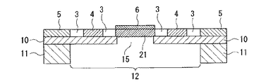
- mirror
- thin film
- scanner
- light reflecting
- reflecting layer
- Prior art date
- Legal status (The legal status is an assumption and is not a legal conclusion. Google has not performed a legal analysis and makes no representation as to the accuracy of the status listed.)
- Withdrawn
Links
- 239000010409 thin film Substances 0.000 claims abstract description 71
- 239000010408 film Substances 0.000 claims description 43
- 229910021420 polycrystalline silicon Inorganic materials 0.000 claims description 16
- 229920005591 polysilicon Polymers 0.000 claims description 16
- 229910021417 amorphous silicon Inorganic materials 0.000 claims description 7
- OKTJSMMVPCPJKN-UHFFFAOYSA-N Carbon Chemical compound [C] OKTJSMMVPCPJKN-UHFFFAOYSA-N 0.000 claims description 6
- 239000002041 carbon nanotube Substances 0.000 claims description 6
- 229910021393 carbon nanotube Inorganic materials 0.000 claims description 6
- 239000011159 matrix material Substances 0.000 claims description 6
- 230000000694 effects Effects 0.000 abstract description 2
- 230000002708 enhancing effect Effects 0.000 abstract description 2
- 230000001965 increasing effect Effects 0.000 description 32
- 238000000034 method Methods 0.000 description 30
- XUIMIQQOPSSXEZ-UHFFFAOYSA-N Silicon Chemical compound [Si] XUIMIQQOPSSXEZ-UHFFFAOYSA-N 0.000 description 14
- 229910052710 silicon Inorganic materials 0.000 description 14
- 239000010703 silicon Substances 0.000 description 14
- VYPSYNLAJGMNEJ-UHFFFAOYSA-N Silicium dioxide Chemical compound O=[Si]=O VYPSYNLAJGMNEJ-UHFFFAOYSA-N 0.000 description 13
- 229910052814 silicon oxide Inorganic materials 0.000 description 13
- 239000000758 substrate Substances 0.000 description 13
- 230000017525 heat dissipation Effects 0.000 description 10
- 238000004519 manufacturing process Methods 0.000 description 10
- 230000015572 biosynthetic process Effects 0.000 description 9
- 238000005530 etching Methods 0.000 description 7
- 238000007788 roughening Methods 0.000 description 6
- 244000126211 Hericium coralloides Species 0.000 description 5
- 238000010438 heat treatment Methods 0.000 description 4
- 239000002184 metal Substances 0.000 description 4
- 229910052751 metal Inorganic materials 0.000 description 4
- 230000005855 radiation Effects 0.000 description 4
- 239000000463 material Substances 0.000 description 3
- XEEYBQQBJWHFJM-UHFFFAOYSA-N Iron Chemical compound [Fe] XEEYBQQBJWHFJM-UHFFFAOYSA-N 0.000 description 2
- PXHVJJICTQNCMI-UHFFFAOYSA-N Nickel Chemical compound [Ni] PXHVJJICTQNCMI-UHFFFAOYSA-N 0.000 description 2
- 239000000470 constituent Substances 0.000 description 2
- 238000000151 deposition Methods 0.000 description 2
- 238000010586 diagram Methods 0.000 description 2
- 239000002048 multi walled nanotube Substances 0.000 description 2
- 229920002120 photoresistant polymer Polymers 0.000 description 2
- CURLTUGMZLYLDI-UHFFFAOYSA-N Carbon dioxide Chemical compound O=C=O CURLTUGMZLYLDI-UHFFFAOYSA-N 0.000 description 1
- 101000617738 Homo sapiens Survival motor neuron protein Proteins 0.000 description 1
- 102100021947 Survival motor neuron protein Human genes 0.000 description 1
- 229910021536 Zeolite Inorganic materials 0.000 description 1
- 235000011089 carbon dioxide Nutrition 0.000 description 1
- 239000003054 catalyst Substances 0.000 description 1
- 230000003197 catalytic effect Effects 0.000 description 1
- 229910017052 cobalt Inorganic materials 0.000 description 1
- 239000010941 cobalt Substances 0.000 description 1
- GUTLYIVDDKVIGB-UHFFFAOYSA-N cobalt atom Chemical compound [Co] GUTLYIVDDKVIGB-UHFFFAOYSA-N 0.000 description 1
- 229910052802 copper Inorganic materials 0.000 description 1
- 230000008021 deposition Effects 0.000 description 1
- HNPSIPDUKPIQMN-UHFFFAOYSA-N dioxosilane;oxo(oxoalumanyloxy)alumane Chemical compound O=[Si]=O.O=[Al]O[Al]=O HNPSIPDUKPIQMN-UHFFFAOYSA-N 0.000 description 1
- PZPGRFITIJYNEJ-UHFFFAOYSA-N disilane Chemical compound [SiH3][SiH3] PZPGRFITIJYNEJ-UHFFFAOYSA-N 0.000 description 1
- 238000001312 dry etching Methods 0.000 description 1
- 238000001704 evaporation Methods 0.000 description 1
- 239000010419 fine particle Substances 0.000 description 1
- 229910052737 gold Inorganic materials 0.000 description 1
- 238000005338 heat storage Methods 0.000 description 1
- 229910052742 iron Inorganic materials 0.000 description 1
- 238000004518 low pressure chemical vapour deposition Methods 0.000 description 1
- 150000002739 metals Chemical class 0.000 description 1
- 238000012986 modification Methods 0.000 description 1
- 230000004048 modification Effects 0.000 description 1
- 229910052759 nickel Inorganic materials 0.000 description 1
- 238000000059 patterning Methods 0.000 description 1
- 230000002093 peripheral effect Effects 0.000 description 1
- 238000000206 photolithography Methods 0.000 description 1
- 238000005268 plasma chemical vapour deposition Methods 0.000 description 1
- 238000009832 plasma treatment Methods 0.000 description 1
- 239000011148 porous material Substances 0.000 description 1
- 238000002360 preparation method Methods 0.000 description 1
- 238000002310 reflectometry Methods 0.000 description 1
- 229910052709 silver Inorganic materials 0.000 description 1
- 239000002109 single walled nanotube Substances 0.000 description 1
- 238000004544 sputter deposition Methods 0.000 description 1
- 239000010457 zeolite Substances 0.000 description 1
Images


Landscapes
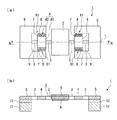
- Laser Beam Printer (AREA)
- Mechanical Optical Scanning Systems (AREA)
- Mechanical Light Control Or Optical Switches (AREA)
- Micromachines (AREA)
- Facsimile Scanning Arrangements (AREA)
Priority Applications (1)
| Application Number | Priority Date | Filing Date | Title |
|---|---|---|---|
| JP2007195513A JP2009031536A (ja) | 2007-07-27 | 2007-07-27 | スキャナ |
Applications Claiming Priority (1)
| Application Number | Priority Date | Filing Date | Title |
|---|---|---|---|
| JP2007195513A JP2009031536A (ja) | 2007-07-27 | 2007-07-27 | スキャナ |
Publications (2)
| Publication Number | Publication Date |
|---|---|
| JP2009031536A true JP2009031536A (ja) | 2009-02-12 |
| JP2009031536A5 JP2009031536A5 (https=) | 2010-07-01 |
Family
ID=40402106
Family Applications (1)
| Application Number | Title | Priority Date | Filing Date |
|---|---|---|---|
| JP2007195513A Withdrawn JP2009031536A (ja) | 2007-07-27 | 2007-07-27 | スキャナ |
Country Status (1)
| Country | Link |
|---|---|
| JP (1) | JP2009031536A (https=) |
Cited By (2)
| Publication number | Priority date | Publication date | Assignee | Title |
|---|---|---|---|---|
| WO2010016480A1 (ja) * | 2008-08-07 | 2010-02-11 | 積水化学工業株式会社 | 絶縁シート及び積層構造体 |
| JP2020086316A (ja) * | 2018-11-29 | 2020-06-04 | 株式会社リコー | 可動装置、画像投影装置、ヘッドアップディスプレイ、レーザヘッドランプ、ヘッドマウントディスプレイ、物体認識装置、及び車両 |
Citations (9)
| Publication number | Priority date | Publication date | Assignee | Title |
|---|---|---|---|---|
| JP2001075029A (ja) * | 1999-09-02 | 2001-03-23 | Sony Corp | マイクロミラーの製造方法 |
| JP2003057566A (ja) * | 2001-08-16 | 2003-02-26 | Furukawa Electric Co Ltd:The | 可変群遅延補償器 |
| JP2003270558A (ja) * | 2002-03-18 | 2003-09-25 | Olympus Optical Co Ltd | 光偏向器及び電磁型アクチュエータ |
| JP2005208608A (ja) * | 2003-12-26 | 2005-08-04 | Sumitomo Precision Prod Co Ltd | マイクロミラースキャナーとその制御方法 |
| JP2005308820A (ja) * | 2004-04-16 | 2005-11-04 | Sumitomo Precision Prod Co Ltd | 静電駆動型memsミラースキャナ |
| JP2006058682A (ja) * | 2004-08-20 | 2006-03-02 | Yokogawa Electric Corp | 光反射素子およびこれを用いた光学装置 |
| JP2006162949A (ja) * | 2004-12-07 | 2006-06-22 | Nippon Signal Co Ltd:The | プレーナ型アクチュエータ |
| WO2006112387A1 (ja) * | 2005-04-15 | 2006-10-26 | Matsushita Electric Industrial Co., Ltd. | 微小機械構造体システムおよびその製造方法 |
| JP2007271909A (ja) * | 2006-03-31 | 2007-10-18 | Victor Co Of Japan Ltd | 光偏向子及びこれを用いた表示装置 |
-
2007
- 2007-07-27 JP JP2007195513A patent/JP2009031536A/ja not_active Withdrawn
Patent Citations (9)
| Publication number | Priority date | Publication date | Assignee | Title |
|---|---|---|---|---|
| JP2001075029A (ja) * | 1999-09-02 | 2001-03-23 | Sony Corp | マイクロミラーの製造方法 |
| JP2003057566A (ja) * | 2001-08-16 | 2003-02-26 | Furukawa Electric Co Ltd:The | 可変群遅延補償器 |
| JP2003270558A (ja) * | 2002-03-18 | 2003-09-25 | Olympus Optical Co Ltd | 光偏向器及び電磁型アクチュエータ |
| JP2005208608A (ja) * | 2003-12-26 | 2005-08-04 | Sumitomo Precision Prod Co Ltd | マイクロミラースキャナーとその制御方法 |
| JP2005308820A (ja) * | 2004-04-16 | 2005-11-04 | Sumitomo Precision Prod Co Ltd | 静電駆動型memsミラースキャナ |
| JP2006058682A (ja) * | 2004-08-20 | 2006-03-02 | Yokogawa Electric Corp | 光反射素子およびこれを用いた光学装置 |
| JP2006162949A (ja) * | 2004-12-07 | 2006-06-22 | Nippon Signal Co Ltd:The | プレーナ型アクチュエータ |
| WO2006112387A1 (ja) * | 2005-04-15 | 2006-10-26 | Matsushita Electric Industrial Co., Ltd. | 微小機械構造体システムおよびその製造方法 |
| JP2007271909A (ja) * | 2006-03-31 | 2007-10-18 | Victor Co Of Japan Ltd | 光偏向子及びこれを用いた表示装置 |
Cited By (3)
| Publication number | Priority date | Publication date | Assignee | Title |
|---|---|---|---|---|
| WO2010016480A1 (ja) * | 2008-08-07 | 2010-02-11 | 積水化学工業株式会社 | 絶縁シート及び積層構造体 |
| JP2020086316A (ja) * | 2018-11-29 | 2020-06-04 | 株式会社リコー | 可動装置、画像投影装置、ヘッドアップディスプレイ、レーザヘッドランプ、ヘッドマウントディスプレイ、物体認識装置、及び車両 |
| JP7247553B2 (ja) | 2018-11-29 | 2023-03-29 | 株式会社リコー | 可動装置、画像投影装置、ヘッドアップディスプレイ、レーザヘッドランプ、ヘッドマウントディスプレイ、物体認識装置、及び車両 |
Similar Documents
| Publication | Publication Date | Title |
|---|---|---|
| JP6539879B2 (ja) | ワイヤグリット型光吸収型偏光素子、透過型プロジェクター、及び液晶表示装置 | |
| US20030016428A1 (en) | Light deflector, method of manufacturing light deflector, optical device using light deflector, and torsion oscillating member | |
| JP6284427B2 (ja) | 光偏向器及びその製造方法 | |
| JP2006003447A (ja) | 偏光分離素子及びその製造方法 | |
| JP4409811B2 (ja) | 光走査装置、光書込装置、画像形成装置、振動ミラーチップ及び光走査モジュール | |
| JPWO2013046612A1 (ja) | 光学反射素子 | |
| EP2701217B1 (en) | Piezoelectric actuator and ink-jet head provided with same | |
| CN101988988B (zh) | 光偏转器、光偏转器的制造方法及图像显示装置 | |
| JP5848504B2 (ja) | 光偏向器 | |
| JP2016212221A (ja) | 光走査装置 | |
| CN101059527A (zh) | 角速度传感器及其制作方法 | |
| JPWO2011152215A1 (ja) | 光走査素子およびそれを用いた画像表示装置 | |
| CN106975838A (zh) | 扫描用反射镜 | |
| JP2017211576A (ja) | 光偏向器及び製造方法 | |
| KR20220146493A (ko) | 펠리클막, 펠리클, 막, 그래핀 시트 및 그 제조 방법 | |
| JP6225544B2 (ja) | 圧電素子の製造方法 | |
| JP2009031536A (ja) | スキャナ | |
| JP2010060592A (ja) | 光学デバイス、光スキャナ及び画像形成装置 | |
| CN106405824B (zh) | 一种复合式压电变形镜 | |
| JP2013225075A (ja) | Mems光スキャナ | |
| JPWO2015145943A1 (ja) | 光走査デバイス | |
| JP2010056379A5 (https=) | ||
| JP2012103469A (ja) | 光学素子および投射型液晶表示装置 | |
| JP2017032627A (ja) | 可動型マイクロミラーデバイス及びその製造方法 | |
| JP4689355B2 (ja) | 周期構造体及び周期構造体による光素子 |
Legal Events
| Date | Code | Title | Description |
|---|---|---|---|
| A521 | Written amendment |
Free format text: JAPANESE INTERMEDIATE CODE: A523 Effective date: 20100514 |
|
| A621 | Written request for application examination |
Free format text: JAPANESE INTERMEDIATE CODE: A621 Effective date: 20100514 |
|
| A977 | Report on retrieval |
Free format text: JAPANESE INTERMEDIATE CODE: A971007 Effective date: 20111226 |
|
| A131 | Notification of reasons for refusal |
Free format text: JAPANESE INTERMEDIATE CODE: A131 Effective date: 20120110 |
|
| A761 | Written withdrawal of application |
Free format text: JAPANESE INTERMEDIATE CODE: A761 Effective date: 20120307 |