JP2009031536A - Scanner - Google Patents
Scanner Download PDFInfo
- Publication number
- JP2009031536A JP2009031536A JP2007195513A JP2007195513A JP2009031536A JP 2009031536 A JP2009031536 A JP 2009031536A JP 2007195513 A JP2007195513 A JP 2007195513A JP 2007195513 A JP2007195513 A JP 2007195513A JP 2009031536 A JP2009031536 A JP 2009031536A
- Authority
- JP
- Japan
- Prior art keywords
- mirror
- thin film
- scanner
- light reflecting
- reflecting layer
- Prior art date
- Legal status (The legal status is an assumption and is not a legal conclusion. Google has not performed a legal analysis and makes no representation as to the accuracy of the status listed.)
- Withdrawn
Links
Images


Abstract
Description
本発明は、プロジェクタやレーザプリンタ等のスキャナエンジンとして適用可能なスキャナに関するものである。 The present invention relates to a scanner applicable as a scanner engine such as a projector or a laser printer.
プロジェクタやレーザプリンタ等のスキャニング方式のひとつとして、スキャニングミラー方式が知られている。スキャニングミラーは、基本構造としてミラー部と、ミラー部を両側から揺動可能に支持する支持部材を有しており、支持部材の弾性を利用して両側の支持部材を貫通する駆動軸周りを揺動する。このようなスキャニングミラーを用いたミラースキャナは、従来のスキャナエンジンであるポリゴンミラースキャナと比べるとモーターが不要であるため小型化が容易という特徴がある。 A scanning mirror method is known as one of scanning methods for projectors and laser printers. As a basic structure, the scanning mirror has a mirror part and a support member that supports the mirror part so that the mirror part can swing from both sides, and swings around the drive shaft that penetrates the support members on both sides by using the elasticity of the support member. Move. A mirror scanner using such a scanning mirror is characterized in that it is easy to miniaturize because it does not require a motor as compared with a polygon mirror scanner which is a conventional scanner engine.
例えば、スキャニングミラー方式のプロジェクタでは、光源としてレーザー光が用いられる。レーザー光は、焦点深度が深いという特長を有しており、その特長を活かすためには光源からのレーザー光を極力絞らずに用いることが望ましい。そのため、スキャニングミラーのミラーサイズは、レーザー光を絞る必要がないだけの十分な大きさが必要となる。 For example, in a scanning mirror type projector, laser light is used as a light source. Laser light has a feature that the depth of focus is deep, and in order to make use of the feature, it is desirable to use the laser light from the light source as much as possible. For this reason, the mirror size of the scanning mirror needs to be large enough that it is not necessary to squeeze the laser beam.
一方、スキャニングミラー方式のプロジェクタでは、画面サイズがミラーの振れ角の大きさに比例する。そのため、大画面の投影のためには、スキャニングミラーの振れ角を大きくとる必要がある。しかし、上記理由から大きなミラーサイズのスキャニングミラーを使用した場合、振れ幅を大きくとると慣性モーメントが大きくなることから、高い駆動電圧が必要となる。 On the other hand, in a scanning mirror type projector, the screen size is proportional to the size of the mirror deflection angle. Therefore, in order to project a large screen, it is necessary to increase the deflection angle of the scanning mirror. However, when a scanning mirror having a large mirror size is used for the above reason, a high driving voltage is required because the moment of inertia increases when the deflection width is increased.
そこで従来は、スキャニングミラーの形状を、揺動運動時の駆動軸方向のミラー長さに対して駆動軸に直交する方向のミラー長さを短く設定し、駆動時の慣性モーメントを小さくすることが提案されていた。この方法によれば、慣性モーメントが小さくなるため、低い駆動電圧でミラーの振れ角を大きくすることが可能となる。また、特許文献1には、スキャニングミラーを支える支持部を工夫することにより、低い駆動電圧でも十分な駆動が可能となる構造が提案されている。
しかしながら、上述の方法では、スキャニングミラーの蓄熱を考慮していないため、低い駆動電圧でスキャニングミラーを駆動させるという点において不十分なものとなっていた。すなわち、レーザー光の照射によりスキャニングミラーの温度が上昇すると、支持部材に熱が伝わり支持部材の温度が上昇する。そうすると、支持部材の弾性定数が低下し、ミラーの振れ角や共振周波数が減少する。この振れ角の減少分は駆動電力を上げることで補正することができるが、その補正分だけ実効電力は低く抑える必要があり、実効電力で駆動可能なサイズにスキャニングミラーを小さく設計せざるを得ない。 However, the above-described method does not take into consideration the heat storage of the scanning mirror, so that it is insufficient in that the scanning mirror is driven with a low driving voltage. That is, when the temperature of the scanning mirror rises due to laser light irradiation, heat is transmitted to the support member, and the temperature of the support member rises. If it does so, the elastic constant of a support member will fall and the deflection angle and resonance frequency of a mirror will reduce. This decrease in deflection angle can be corrected by increasing the drive power, but the effective power needs to be kept low by that correction, and the scanning mirror must be designed to be small enough to be driven with effective power. Absent.
本発明はこのような事情に鑑みてなされたものであって、スキャニングミラーの放熱効果を高め、低い駆動電圧で安定したミラー駆動が可能なスキャナを提供することを目的とする。 The present invention has been made in view of such circumstances, and an object of the present invention is to provide a scanner capable of enhancing the heat dissipation effect of a scanning mirror and capable of stable mirror driving with a low driving voltage.
上記の課題を解決するため、本発明の第1のスキャナは、表面に光反射層が形成されたミラーと、前記ミラーを所定の駆動軸の周りに揺動駆動させる駆動部と、を備え、前記ミラーの前記光反射層とは反対側の面に、前記ミラーよりも熱伝導率の高い薄膜が形成されていることを特徴とする。
この構成によれば、レーザー光によりミラーに蓄熱した熱を、形成された薄膜を介して効率的に放熱することができる。そのため、ミラーの温度上昇に対応する補正電力が減少し若しくは不要となり、実効電力を高めることができる。その結果、ミラーのサイズを大きくすることが可能になり、低い電圧で安定したミラー駆動が可能なミラースキャナを提供することが可能となる。
In order to solve the above problems, a first scanner of the present invention includes a mirror having a light reflection layer formed on a surface thereof, and a drive unit that drives the mirror to swing around a predetermined drive axis. A thin film having a thermal conductivity higher than that of the mirror is formed on a surface of the mirror opposite to the light reflecting layer.
According to this configuration, the heat stored in the mirror by the laser light can be efficiently radiated through the formed thin film. Therefore, the correction power corresponding to the temperature rise of the mirror is reduced or unnecessary, and the effective power can be increased. As a result, it is possible to increase the size of the mirror, and it is possible to provide a mirror scanner capable of stable mirror driving with a low voltage.
本発明の第2のスキャナは、表面に光反射層が形成されたミラーと、前記ミラーを所定の駆動軸の周りに揺動駆動させる駆動部と、を備え、前記ミラーの前記光反射層とは反対側の面に、粗面化処理が施されていることを特徴とする。
この構成によれば、前記ミラーの表面積が広がるため、レーザー光によりミラーに蓄熱した熱を効率的に放熱することができる。そのため、ミラーの温度上昇に対応する補正電力が減少し若しくは不要となり、実効電力を高めることができる。その結果、ミラーのサイズを大きくすることが可能になり、低い電圧で安定したミラー駆動が可能なミラースキャナを提供することが可能となる。
A second scanner according to the present invention includes a mirror having a light reflection layer formed on a surface thereof, and a drive unit that drives the mirror to swing around a predetermined drive axis, the light reflection layer of the mirror, Is characterized in that the opposite surface is subjected to a roughening treatment.
According to this configuration, since the surface area of the mirror is increased, the heat stored in the mirror by the laser light can be efficiently radiated. Therefore, the correction power corresponding to the temperature rise of the mirror is reduced or unnecessary, and the effective power can be increased. As a result, it is possible to increase the size of the mirror, and it is possible to provide a mirror scanner capable of stable mirror driving with a low voltage.
本発明の第3のスキャナは、表面に光反射層が形成されたミラーと、前記ミラーを所定の駆動軸の周りに揺動駆動させる駆動部と、を備え、前記ミラーの光反射層とは反対側の面に、表面に微細な凹凸が形成された薄膜が形成されていることを特徴とする。
この構成によれば、前記ミラーの表面積が広がるため、レーザー光によりミラーに蓄熱した熱を効率的に放熱することができる。そのため、ミラーの温度上昇に対応する補正電力が減少し若しくは不要となり、実効電力を高めることができる。その結果、ミラーのサイズを大きくすることが可能になり、低い電圧で安定したミラー駆動が可能なミラースキャナを提供することが可能となる。
A third scanner of the present invention includes a mirror having a light reflecting layer formed on a surface thereof, and a driving unit that drives the mirror to swing around a predetermined driving axis. What is the light reflecting layer of the mirror? A thin film having fine irregularities formed on the surface is formed on the opposite surface.
According to this configuration, since the surface area of the mirror is increased, the heat stored in the mirror by the laser light can be efficiently radiated. Therefore, the correction power corresponding to the temperature rise of the mirror is reduced or unnecessary, and the effective power can be increased. As a result, it is possible to increase the size of the mirror, and it is possible to provide a mirror scanner capable of stable mirror driving with a low voltage.
本発明においては、前記ミラーの駆動軸上には、前記ミラーを静電駆動するための静電容量素子部が接続され、前記静電容量素子部の、光の入射側とは反対側の面に、前記静電容量素子部よりも熱伝導率の高い薄膜が形成されていることが望ましい。
この構成によれば、前記静電容量素子部からも放熱が可能になり、更に放熱効率が高まる。
In the present invention, a capacitive element for electrostatically driving the mirror is connected on the drive shaft of the mirror, and the surface of the capacitive element opposite to the light incident side In addition, it is desirable that a thin film having a higher thermal conductivity than the capacitance element portion is formed.
According to this configuration, it is possible to dissipate heat from the capacitance element portion, and the heat dissipation efficiency is further increased.
本発明においては、前記ミラーの前記光反射層とは反対側の面に凹部が形成されていることが望ましい。
この構成によれば、凹部により前記ミラーの表面積が広がるため、ミラーの放熱効率が更に高まる。また、凹部を形成することにより、ミラーが軽量化できるため、低い電圧で安定したミラー駆動が可能なミラースキャナを提供することが可能となる。
In the present invention, it is desirable that a recess is formed on the surface of the mirror opposite to the light reflecting layer.
According to this configuration, since the surface area of the mirror is expanded by the recess, the heat dissipation efficiency of the mirror is further increased. In addition, since the mirror can be reduced in weight by forming the concave portion, it is possible to provide a mirror scanner capable of stable mirror driving with a low voltage.
本発明においては、前記薄膜は、アモルファスシリコン膜を熱処理して形成されたポリシリコン膜であることが望ましい。
アモルファスシリコン膜は熱処理の条件によって緻密なポリシリコン膜から表面の粗いポリシリコン膜まで、その表面形状を大きく変動させることができる。本発明では、ポリシリコン膜の膜密度が粗くなる(若しくは多孔質となる)ような条件でアモルファスシリコン膜を熱処理し、それによって、ミラーの裏面に粗面化された薄膜を形成している。この構成によれば、薄膜がポリシリコン膜で形成されるため、シリコン基板によってミラーを形成した場合に、薄膜とミラーとの密着力が高まる。そのため、信頼性に優れたスキャナが提供できる。
In the present invention, the thin film is preferably a polysilicon film formed by heat-treating an amorphous silicon film.
The surface shape of an amorphous silicon film can vary greatly from a dense polysilicon film to a rough polysilicon film depending on the heat treatment conditions. In the present invention, the amorphous silicon film is heat-treated under conditions such that the film density of the polysilicon film becomes rough (or becomes porous), thereby forming a roughened thin film on the back surface of the mirror. According to this configuration, since the thin film is formed of the polysilicon film, when the mirror is formed by the silicon substrate, the adhesion between the thin film and the mirror is increased. Therefore, a scanner with excellent reliability can be provided.
本発明においては、前記薄膜は、カーボンナノチューブの薄膜であることが望ましい。
この構成によれば、柱状のカーボンナノチューブが薄膜状に形成されるため、ミラーの表面積が著しく広がる。そのため、非常に高い放熱効率を実現することができる。
In the present invention, the thin film is preferably a carbon nanotube thin film.
According to this configuration, since the columnar carbon nanotubes are formed in a thin film shape, the surface area of the mirror is significantly increased. Therefore, very high heat dissipation efficiency can be realized.
本発明においては、前記ミラーを前記駆動軸の周りに揺動可能に支持する支持部材が設けられ、前記薄膜は、前記支持部材を除く部分に形成されていることが望ましい。
この構成によれば、支持部材に薄膜が形成されないため、支持部材の弾性率の低下を防ぎ、ミラーの振れ角の減少を防ぐことが出来る。
In the present invention, it is preferable that a support member for supporting the mirror so as to be swingable around the drive shaft is provided, and the thin film is formed in a portion excluding the support member.
According to this configuration, since a thin film is not formed on the support member, it is possible to prevent a decrease in the elastic modulus of the support member and to prevent a decrease in the deflection angle of the mirror.
本発明においては、前記凹部は、マトリクス状に配列されるように形成されていることが望ましい。
この構成によれば、凹部がマトリクス状に多数形成されることで、更にミラーの表面積(放熱効率)を高めることができる。また、凹部の形成されない部分(厚みの厚い部分)が縦横に形成されるため、その部分が梁の役割を果たし、凹部形成によるミラーの強度低下を防ぐことができる。そのため、信頼性が高く、安定したミラー駆動が可能なスキャナが提供できる。
In the present invention, the recesses are preferably formed so as to be arranged in a matrix.
According to this configuration, the surface area (heat radiation efficiency) of the mirror can be further increased by forming a large number of recesses in a matrix. In addition, since the portion where the concave portion is not formed (thick portion) is formed vertically and horizontally, the portion serves as a beam, and the reduction in the strength of the mirror due to the concave portion formation can be prevented. Therefore, a scanner with high reliability and capable of stable mirror driving can be provided.
本発明においては、前記凹部は、ハニカム状に配列されるように形成されていることが望ましい。
この構成によれば、凹部がハニカム状に多数形成されることで、更にミラーの表面積(放熱効率)を高めることができる。また、凹部の形成されない部分(厚みの暑い部分)が縦横に形成されるため、その部分が梁の役割を果たし、凹部形成によるミラーの強度低下を防ぐことができる。そのため、信頼性が高く、安定したミラー駆動が可能なスキャナが提供できる。
In the present invention, the recesses are preferably formed so as to be arranged in a honeycomb shape.
According to this configuration, the surface area (heat dissipation efficiency) of the mirror can be further increased by forming a large number of recesses in a honeycomb shape. In addition, since the portion where the concave portion is not formed (the portion where the thickness is hot) is formed vertically and horizontally, the portion serves as a beam, and it is possible to prevent a reduction in the strength of the mirror due to the concave portion formation. Therefore, a scanner with high reliability and capable of stable mirror driving can be provided.
本発明においては、前記凹部は、前記駆動軸に対して対称に配置されていることが望ましい。
この構成によれば、凹部を形成したミラーの慣性モーメントが駆動軸を挟んで対称となるため、駆動時の不具合をなくすことができる。
In the present invention, it is desirable that the recesses are arranged symmetrically with respect to the drive shaft.
According to this configuration, since the moment of inertia of the mirror formed with the recesses is symmetric with respect to the drive shaft, problems during driving can be eliminated.
[第1実施形態]
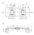
以下、図1を参照しながら、本発明の第1実施形態に係るスキャナについて説明する。図1(a)は本実施形態のスキャナを光反射層側から見た平面図であり、図1(b)は図1(a)のIbで結ばれる線での断面図である。なお、以下の全ての図面においては、図面を見やすくするため、各構成要素の膜厚や寸法の比率などは適宜異ならせてある。
[First Embodiment]
The scanner according to the first embodiment of the present invention will be described below with reference to FIG. FIG. 1A is a plan view of the scanner of this embodiment as viewed from the light reflecting layer side, and FIG. 1B is a cross-sectional view taken along the line Ib in FIG. In all the drawings below, the film thicknesses and dimensional ratios of the constituent elements are appropriately changed in order to make the drawings easy to see.
図1(a)に示すように、本実施形態におけるスキャナ1は、ミラー2と、ミラー2を支持する支持部材3と、支持部材3と一体として設けられている静電容量素子部4と、ミラー2が支持部材3を介して接続するフレーム5と、を備えている。
As shown in FIG. 1A, the
スキャナ1は、中央部に矩形のミラー2を備えている。ミラー2の形状は、矩形以外にも目的に応じて、菱形、多角形、円形、楕円を適宜採用できる。ミラー2の対向した2つの端部の中央部に、2つの支持部材3がミラー2を挟み込むように結合している。各支持部材3の中央部には静電容量素子部4が設けられている。更に、支持部材3が結合したミラー2を挟み込むように一対のフレーム5が配置され、支持部材3を介してミラー2が一対のフレーム5に結合している。一対の支持部材3は、ミラー2を挟んで同一直線状に配置されており、ミラー2が揺動する際には該直線を駆動軸Lとして揺動する。
The
支持部材3は、梁状の基板である。本実施形態では、各支持部材3の長手方向中央部に、静電容量素子部4が形成されている。静電容量素子部4は、矩形の本体部41と、本体部41の外周部に設けられた揺動側櫛歯部42とを備えている。本体部41は中心が駆動軸L上に配置され、その平行な一対の辺が駆動軸Lと平行に配置されている。揺動側櫛歯部42は、その駆動軸Lと平行に配置された一対の辺にそれぞれ設けられている。揺動側櫛歯部42は、本体部41から駆動軸Lと直交する方向に突出する複数の揺動側櫛歯7を備えており、該複数の揺動側櫛歯7が駆動軸Lと平行に配列されることにより、全体としての揺動側櫛歯部42が形成されている。本体部41の一対の辺に設けられた一対の揺動側櫛歯部42は、駆動軸Lを中心として線対称な構成となっている。
The
フレーム5は、矩形の一辺に凹部Hが形成された平面視コ字型の形状を有する。一対のフレーム5は、互いの凹部Hがミラー2を挟んで対向するように配置されており、各フレーム5の凹部Hの底部中央部には支持部材3が接続されている。フレーム5には、支持部材3を介してミラー2が支持されている。フレーム5の凹部Hにおいて支持部材3が接続されていない一対の辺には、複数の固定側櫛歯8からなる一対の固定側櫛歯部81が形成されている。フレーム5の複数の固定側櫛歯8と、静電容量素子部4の複数の揺動側櫛歯7とは、微小な隙間を隔てて噛み合うように交互に配置されている。この固定側櫛歯部81と揺動側櫛歯部42とが一対で駆動部を構成する。なお、図1では、フレーム5は、ミラー2を挟んで2つ設けられているが、平面視輪帯状の単一のフレームがミラー2の周囲を囲んで配置されていても良い。
The
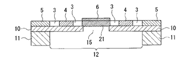
図1(b)に示すように、ミラー2の一方の面には、全面にレーザー光に対し十分な反射率を持つ光反射層6が設けられている。本実施形態では例えばAlを蒸着することにより、光反射層6が形成されている。光反射層6は、本実施形態のようにたとえばAlのような金属薄膜をミラー2の表面に成膜して形成しても良く、また、多層反射膜を成膜する方法で形成しても良く、更には、金属薄膜を成膜せずにミラー2の表面を研磨して形成してもよい。ミラー2の光反射層6とは反対の面には、ミラー2よりも熱伝導率が良い物質からなる薄膜9がほぼ全面に形成されている。本実施形態ではAlで薄膜9を形成しているが、Au、Ag、Cuなどを成膜しても良い。ミラー2と光反射層6とをあわせた厚みは例えば60μmであり、薄膜9の厚みは例えば1μmである。
As shown in FIG. 1B, a
ミラー2と、支持部材3と、静電容量素子部4と、フレーム5と、は全て同一平面上に配置されている。フレーム5は、酸化シリコン膜10上に形成されており、酸化シリコン膜10の下層側にはシリコン層11からなるシリコン基板部が設けられている。シリコン層11、酸化シリコン膜10及びフレーム5は平面視同一形状にパターニングされており、ミラー2、支持部材3及び静電容量素子部4の下層側の酸化シリコン膜10及びシリコン層11は全て除去されている。
The
以上図面に基づいて本実施形態のスキャナ1を説明してきたが、次に、このスキャナ1の製造方法を説明する。
The
図2及び3は、本実施形態のスキャナ11の製造工程を示す工程断面図である。図2及び図3の各図は、図1のIbで結ばれる線での断面に対応する断面図であり、図2は、ミラー2の光反射層6とは反対の面へ薄膜9を形成するための準備工程、図3は、ミラー2へ薄膜9を形成しスキャナ1とする工程を示す。
2 and 3 are process cross-sectional views illustrating the manufacturing process of the
まず図2(a)に示すように、第1の工程として、SOI基板の片方の面にエッチングを施し、SOI基板のシリコン層に、所望のミラー2と支持部材3と静電容量素子部4とフレーム5と、を形成する。この工程は従来公知の方法により容易に実施できる工程であり、例えばフォトリソグラフィ法によりパターニングして作成したマスクを介してドライエッチングを施すことにより形成することができる。次いで、ミラー2の全面にAlを蒸着させて光反射層6を形成する。
First, as shown in FIG. 2A, as a first step, etching is performed on one surface of the SOI substrate, and a desired
次いで、図2(b)に示すように、第2の工程として、第1の工程で加工を施したSOI基板の面とは反対の面に図示略の第1マスクを形成してエッチングを施し、形成したフレーム5に平面的に重なる箇所を残して、シリコン層11を除去し、第1開口部12を形成する。次いで第1マスクを除去する。
Next, as shown in FIG. 2B, as a second step, etching is performed by forming a first mask (not shown) on the surface opposite to the surface of the SOI substrate processed in the first step. The
次いで、図2(c)に示すように、第3の工程として、第1開口部12の底面に露出した酸化シリコン膜10上に、形成したミラー2と平面的に重なる箇所に第2開口部14を設けた第2マスク13を付す。第2マスク13は、例えばフォトレジストを塗布して、開口部14を形成するように硬化させて形成する。
Next, as shown in FIG. 2C, as a third step, the second opening is formed at a position overlapping the formed
次いで、図2(d)に示すように、第4の工程として、第3の工程で付した第2マスクを介して酸化シリコン膜10にエッチングを施し、ミラー2に平面的に重なる部分を除去する。エッチングが進行すると、酸化シリコン膜10に第3開口部15が形成され、ミラー2の光反射層6を形成した面とは反対の面が露出する。次いで第2マスクを除去する。以上のようにして、ミラー2の光反射層6とは反対の面へ薄膜を形成するための準備が整う。
Next, as shown in FIG. 2D, as a fourth step, the
次いで、図3(a)に示すように、第5の工程として、光反射層6を形成した面とは反対側の、第3開口部15の底部に露出したシリコン層、第1開口部12の底部に露出した酸化シリコン膜10、フレーム5に平面的に重なるシリコン層11、の水平面にスパッタ法を用いてAlを堆積させ薄膜9を形成する。
Next, as shown in FIG. 3A, as a fifth step, the silicon layer exposed at the bottom of the
次いで、図3(b)に示すように、第6の工程として、酸化シリコン膜10に形成された第3開口部15を第3マスク16で保護する。本実施形態では、第3開口部15に形成した薄膜9の上に第3マスク16が形成される。第3マスク16は、例えばフォトレジストを塗布して硬化させて形成する。
Next, as shown in FIG. 3B, as a sixth step, the
次いで、図3(c)に示すように、第7の工程として、第6の工程で付した第3マスク16を介してエッチングを施し、第3マスク16で覆われた薄膜9を残して他の箇所に形成された薄膜9を除去する。更に、エッチングを施し、第1開口部12の底部に露出する酸化シリコン膜10を除去する。
Next, as shown in FIG. 3C, as a seventh step, etching is performed through the
次いで、図3(d)に示すように、第8の工程として、薄膜9上の第3マスクを除去する。以上のようにして、本実施形態のスキャナ1が完成する。
Next, as shown in FIG. 3D, as the eighth step, the third mask on the
以上のような構成のスキャナ1によれば、レーザー光によりミラー2に蓄熱した熱を、形成された薄膜9を介して効率的に放熱することができる。そのため、ミラー2の温度上昇に対応する補正電力が減少し若しくは不要となり、実効電力を高めることができる。その結果、ミラー2のサイズを大きくすることが可能になり、低い電圧で安定したミラー駆動が可能なミラースキャナを提供することが可能となる。
According to the
また、本実施形態では、支持部材3に薄膜9が形成されないため、支持部材3の弾性率の低下を防ぎ、ミラー2の振れ角の減少を防ぐことが出来る。
Further, in the present embodiment, since the
なお、本実施形態では、ミラー2にだけ薄膜9を形成することとしたが、静電容量素子部4にも薄膜を形成するとなお良い。そうすると静電容量素子部4からも放熱が可能になり、更に放熱効率が高まる。その場合は、図4(a)に示すように、第3の工程において静電容量素子部4と平面的に重なる箇所にも開口部18を設けたマスク17を形成し、後の工程を同様に実施することで、図4(b)に示すように、静電容量素子部4の、光反射層6への光の入射側とは反対側の面に薄膜9が形成された形態のスキャナ19が完成する。
In the present embodiment, the
[第2実施形態]
図5は、本発明の第2実施形態に係るスキャナの、図1(b)に対応する断面図である。本実施形態のスキャナの構成は、第1実施形態のスキャナと一部共通している。異なるのは、ミラーの光反射層とは反対側の面に、ミラーよりも熱伝導率の高い薄膜が形成されておらず、粗面化処理が施されていることである。したがって、本実施形態において第1実施形態と共通する構成要素については同じ符号を付し、詳細な説明は省略する。ここで粗面化処理とは、平坦な面に対して物理的な処理を施すことにより、もとの平坦な面に微細な凹凸を無数に付すことを指す。
[Second Embodiment]
FIG. 5 is a sectional view corresponding to FIG. 1B of a scanner according to the second embodiment of the present invention. The configuration of the scanner of the present embodiment is partially in common with the scanner of the first embodiment. The difference is that a thin film having a higher thermal conductivity than that of the mirror is not formed on the surface of the mirror opposite to the light reflecting layer, and the surface is roughened. Therefore, in this embodiment, the same code | symbol is attached | subjected about the component which is common in 1st Embodiment, and detailed description is abbreviate | omitted. Here, the roughening treatment refers to applying innumerable fine irregularities to the original flat surface by performing physical treatment on the flat surface.
図5に示すように、本実施形態のスキャナ20は、ミラー21の光反射層6とは反対側の面が粗面化処理され、微細な凹凸が無数に付されている。
As shown in FIG. 5, in the
その製造工程は、図6に示すように、第1実施形態で説明した方法を用いてSOI基板に第3開口部15を形成し、第1実施形態で行った薄膜形成の替わりに第3開口部15の底面に露出したシリコン層表面に粗面化処理を行う。その後の工程は第1実施形態で説明した方法にて製造することにより、本実施形態のスキャナ20が完成する。粗面化処理の方法としては、例えばドライアイスを用いたブラスト処理、ブラシスクラブ処理、プラズマ処理等の方法が挙げられる。本実施形態では、ミラー21の光反射層6とは反対側の面のみ粗面化処理を行い製造することとしたが、粗面化処理が、第1開口部12に露出した酸化シリコン膜10上に及んでも構わない。
As shown in FIG. 6, in the manufacturing process, the
以上のような構成のスキャナ20によれば、ミラー21の表面積が広がるため、レーザー光によりミラー21に蓄熱した熱を効率的に放熱することができる。そのため、ミラー21の温度上昇に対応する補正電力が減少し若しくは不要となり、実効電力を高めることができる。その結果、ミラー21のサイズを大きくすることが可能になり、低い電圧で安定したミラー駆動が可能なミラースキャナを提供することが可能となる。
According to the
なお、本実施形態でも第1実施形態と同様に、静電容量素子部4にも粗面化処理をするとなお良い。静電容量素子部4からも放熱が可能になり、更に放熱効率が高まる。
In the present embodiment as well, as in the first embodiment, it is better to roughen the
[第3実施形態]
図7は、本発明の第3実施形態に係るスキャナの、図1(b)に対応する断面図である。本実施形態のスキャナの構成は、第1実施形態のスキャナと一部共通している。異なるのは、ミラーの光反射層とは反対側の面に形成される薄膜が、その形成過程において膜表面に微細な凹凸を形成しながら成長する、化学的に粗面化された粗面化薄膜であることである。したがって、本実施形態において第1実施形態と共通する構成要素については同じ符号を付し、詳細な説明は省略する。
[Third Embodiment]
FIG. 7 is a cross-sectional view corresponding to FIG. 1B of a scanner according to the third embodiment of the present invention. The configuration of the scanner of the present embodiment is partially in common with the scanner of the first embodiment. The difference is that the thin film formed on the surface opposite to the light reflecting layer of the mirror grows while forming fine irregularities on the film surface during the formation process, and the surface is chemically roughened. It is a thin film. Therefore, in this embodiment, the same code | symbol is attached | subjected about the component which is common in 1st Embodiment, and detailed description is abbreviate | omitted.
図7に示すように、本実施形態のスキャナ22は、ミラー23の光反射層6とは反対側の面に微細な凹凸が形成された粗面化薄膜24が形成されている。本実施形態では、粗面化薄膜24として粗面化ポリシリコン膜が形成されている。
As shown in FIG. 7, the
その製造工程は、図8に示すように、第1実施形態で説明した方法を用いてSOI基板に第3開口部15を形成し、第1実施形態で行った熱伝導率の高い物質の薄膜形成の替わりに、粗面化薄膜24として粗面化ポリシリコン膜を形成し、その後の工程は第1実施形態で説明した方法にて製造することにより、本実施形態のスキャナ22が完成する。粗面化ポリシリコン膜は、例えば、縦型炉を用いて、1mTorrの真空中にジシランガス(Si2H6)を5sccm導入し、約750℃〜800℃にて60分間熱処理を施す。この熱処理によって、アモルファスシリコン膜がポリシリコン膜に結晶化する過程において、表面にグレインに起因した凹凸が形成される。また他にも、チューブ式の減圧CVD装置で、成膜温度=575℃、デポジション圧力=0.2Torrの条件下で成膜することにより、粗面化ポリシリコン膜を形成することもできる。
As shown in FIG. 8, in the manufacturing process, the
アモルファスシリコン膜は熱処理の条件によって緻密なポリシリコン膜から表面の粗いポリシリコン膜まで、その表面形状を大きく変動させることができる。本実施形態では、ポリシリコン膜の膜密度が粗くなる(若しくは多孔質となる)ような条件でアモルファスシリコン膜を熱処理し、それによって、ミラー23の裏面に粗面化された粗面化薄膜24を形成している。この構成によれば、粗面化薄膜24がポリシリコン膜で形成されるため、シリコン基板によってミラー23を形成した場合に、粗面化薄膜24とミラー23との密着力が高まる。そのため、信頼性に優れたスキャナ22が提供できる。
The surface shape of an amorphous silicon film can vary greatly from a dense polysilicon film to a rough polysilicon film depending on the heat treatment conditions. In the present embodiment, the amorphous silicon film is heat-treated under the condition that the film density of the polysilicon film becomes rough (or becomes porous), whereby the roughened
なお、本実施形態においては、粗面化ポリシリコン膜を形成することとしたが、本実施形態の粗面化薄膜24としてカーボンナノチューブを形成することとしても構わない。カーボンナノチューブは、例えば、触媒金属としてニッケルを形成し、続いて、高周波マグネトロン型プラズマCVD装置を用い、RF電力=900W、基板温度=850℃、ガス圧力=0.5Torr、混合ガス比CH4/H2=9/1で10分間処理を行うことにより、多層カーボンナノチューブ(MWNTs)を成長させ形成する。また他にも、多孔質物質のゼオライト表面に触媒金属である鉄およびコバルトの微粒子金属を保持させ、CH4とH2の混合ガス(ガス比=3/7)、基板温度550℃で処理することにより、高い熱伝導性を持つ単層カーボンナノチューブ(SMNT)を成長させることもできる。
この構成によれば、柱状のカーボンナノチューブが薄膜状に形成されるため、ミラー23の表面積が著しく広がる。そのため、非常に高い放熱効率を実現することができる。
In the present embodiment, the roughened polysilicon film is formed. However, carbon nanotubes may be formed as the roughened
According to this configuration, since the columnar carbon nanotubes are formed in a thin film shape, the surface area of the
また、本実施形態では、支持部材3に粗面化薄膜24が形成されないため、支持部材3の弾性率の低下を防ぎ、ミラー23の振れ角の減少を防ぐことが出来る。
Further, in the present embodiment, since the roughened
[第4実施形態]
図9は、本発明の第4実施形態に係るスキャナの説明図であり、(a)が平面図、(b)が図9(a)のIXbで結ばれる線での断面図である。本実施形態のスキャナの構成は、第1実施形態のスキャナと一部共通している。異なるのは、ミラーよりも熱伝導率の高い薄膜が形成される前に、ミラーの光反射層とは反対側の面に複数の凹部を設けることである。したがって、本実施形態において第1実施形態と共通する構成要素については同じ符号を付し、詳細な説明は省略する。
[Fourth Embodiment]
FIG. 9 is an explanatory diagram of a scanner according to the fourth embodiment of the present invention, in which (a) is a plan view and (b) is a cross-sectional view taken along the line IXb in FIG. 9 (a). The configuration of the scanner of the present embodiment is partially in common with the scanner of the first embodiment. The difference is that a plurality of recesses are provided on the surface of the mirror opposite to the light reflecting layer before the thin film having higher thermal conductivity than the mirror is formed. Therefore, in this embodiment, the same code | symbol is attached | subjected about the component which is common in 1st Embodiment, and detailed description is abbreviate | omitted.
図9(a)に示すように、本実施形態のスキャナ25は、平面図では図1(a)に示す第1実施形態のスキャナ1と基本的構成が同じである。しかし本実施形態のスキャナ25は、ミラー26の光反射層とは反対側の面に複数の凹部27が設けられている。凹部27は平面視正方形であり、マトリクス状に縦横に配列している。ミラー26の光反射部とは反対の面の、凹部27を形成していない部分26A(厚みの厚い部分)は平面視格子状に設けられている。凹部27は、駆動軸Lに対して線対称になるように配置されている。
As shown in FIG. 9A, the basic configuration of the
図9(b)に示すように、ミラー26の光反射層6とは反対の面には、ミラー26よりも熱伝導率が良い物質からなる薄膜28がほぼ全面に形成されている。薄膜28は凹部27の側壁や底部にも形成している。本実施形態ではAlで薄膜28を形成する。
As shown in FIG. 9B, a thin film 28 made of a material having a thermal conductivity better than that of the
図10は本実施形態のスキャナ25の製造工程を示す工程断面図である。まず、図10(a)に示すように、第1実施形態で説明した方法にて、第1開口部12を形成したSOI基板を用意し、光反射層6を形成した面とは反対の面に露出した酸化シリコン膜10において光反射層6と平面的に重なる箇所に、所望の凹部に対応するパターンを付したマスク29を形成する。
FIG. 10 is a process cross-sectional view showing the manufacturing process of the
次いで、図10(b)に示すように、マスク29を介してエッチングを施し、ミラー26に平面的に重なる酸化シリコン膜10を除去するとともに、シリコン層をエッチングする。エッチングが進行すると、マスク29のパターンに沿って光反射層6とは反対側の面のシリコン層に複数の凹部27が設けられ、ミラー26が形成される。以上のようにして、ミラー26の光反射層6の形成されていない面へ凹部27を形成したら、第1実施形態で説明した方法にてミラー26の光反射層6とは反対側の面に熱伝導率の高い薄膜28(図9(b)参照)を形成する。以上により、本実施形態のスキャナ25が完成する。
Next, as shown in FIG. 10B, etching is performed through a
以上のような構成のスキャナ25によれば、ミラー26の裏面にマトリクス状に多数の凹部27が形成されているため、ミラー26の表面積が広がり、ミラー26の放熱効率が更に高まる。
According to the
また、凹部27を形成することにより、ミラー26が軽量化できるため、低い電圧で安定したミラー駆動が可能なミラースキャナを提供することが可能となる。その上、本実施形態では、凹部27の形成されない部分26A(厚みの厚い部分)が縦横に形成されるため、その部分が梁の役割を果たし、凹部27の形成によるミラー26の強度低下を防ぐことができる。そのため、信頼性が高く、安定したミラー駆動が可能なスキャナ25が提供できる。
Moreover, since the
また、本実施形態では、凹部27は駆動軸Lに対して対称に配置されていることとしたため、凹部27を形成したミラー26の慣性モーメントが駆動軸Lを挟んで対称となり、駆動時の不具合をなくすことができる。
In the present embodiment, since the
また、本実施形態では、支持部材3に薄膜28が形成されないため、支持部材3の弾性率の低下を防ぎ、ミラー26の振れ角の減少を防ぐことが出来る。
Further, in the present embodiment, since the thin film 28 is not formed on the
なお、本実施形態においては、凹部は、マトリクス状に配列されるように形成されていることとしたが、ハニカム状に配列されるように形成されていることとしても構わない。 In the present embodiment, the concave portions are formed so as to be arranged in a matrix shape, but may be formed so as to be arranged in a honeycomb shape.
図11は、本発明の第4実施形態に係るスキャナの凹部が別形状である場合の説明図である。図11(a)がスキャナ30の平面図、(b)が図11(a)のXIbで結ばれる線での断面図である。図11(a)に示すように、ミラー31に設けられた凹部32は平面視六角形であり、縦横に配列している。ミラー31を構成する基板の、凹部32を形成していない部分は平面視ハニカム状に設けられている。凹部32は、駆動軸Lに対して対称になるように配置されている。
FIG. 11 is an explanatory diagram when the concave portion of the scanner according to the fourth embodiment of the present invention has a different shape. 11A is a plan view of the
図11(b)に示すように、ミラー31の光反射層6とは反対の面には、ミラー31よりも熱伝導率が良い薄膜33がほぼ全面に形成してある。薄膜33は凹部32の側壁や底部にも形成されている。本実施形態ではAlで薄膜33を形成する。
As shown in FIG. 11B, a
この構成によれば、凹部32がハニカム状に多数形成されることで、更にミラー31の表面積が広がり、放熱効率が高まる。また、凹部32の形成されない部分(厚みの厚い部分)が縦横に形成されるため、その部分が梁の役割を果たし、凹部32形成によるミラー31の強度低下を防ぐことができる。そのため、信頼性が高く、安定したミラー駆動が可能なスキャナ30が提供できる。
According to this configuration, since a large number of the
なお、本実施形態でも第1実施形態と同様に、静電容量素子部4にも薄膜33を形成するとなお良い。静電容量素子部4からも放熱が可能になり、更に放熱効率が高まる。
In this embodiment as well, as in the first embodiment, it is better to form the
また、本実施形態においては、凹部32を形成した後に熱伝導率の高い薄膜33を形成することとしたが、光反射層6とは反対の面を粗面化処理しても良い。その場合、ミラー31の表面積を更に広げ、放熱効率を高めることができる。
In the present embodiment, the
また、本実施形態においては、凹部32を形成した後に熱伝導率の高い薄膜33を形成することとしたが、光反射層6とは反対の面に表面に微細な凹凸が形成された薄膜を付ししても良い。その場合、ミラー31の表面積を更に広げ、放熱効率を高めることができる。
In the present embodiment, the
また、本実施形態においては、凹部32を形成した後に熱伝導率の高い薄膜33を形成することとしたが、薄膜33を形成した後に凹部32を形成することとしても構わない。
In the present embodiment, the
また、凹部32の形状は本実施形態で示した形状に限定されず、例えば、平面視円形、矩形などであってもかまわない。
Moreover, the shape of the recessed
以上、添付図面を参照しながら本発明に係る好適な実施の形態例について説明したが、本発明は係る例に限定されないことは言うまでもない。上述した例において示した各構成部材の諸形状や組み合わせ等は一例であって、本発明の主旨から逸脱しない範囲において設計要求等に基づき種々変更可能である。 The preferred embodiments of the present invention have been described above with reference to the accompanying drawings, but it goes without saying that the present invention is not limited to such examples. Various shapes, combinations, and the like of the constituent members shown in the above-described examples are examples, and various modifications can be made based on design requirements and the like without departing from the gist of the present invention.
1、19、20、22、25、30…スキャナ、 2、21、23、26、31…ミラー、 4…静電容量素子部、6…光反射層、 7…揺動側櫛歯(駆動部)、 8…固定側櫛歯(駆動部)、 9、28、33…薄膜、 24…粗面化薄膜、 27、32…凹部、
DESCRIPTION OF
Claims (11)
前記ミラーを所定の駆動軸の周りに揺動駆動させる駆動部と、を備え、
前記ミラーの前記光反射層とは反対側の面に、前記ミラーよりも熱伝導率の高い薄膜が形成されていることを特徴とするスキャナ。 A mirror having a light reflecting layer formed on the surface;
A drive unit that swings and drives the mirror around a predetermined drive shaft,
A scanner, wherein a thin film having higher thermal conductivity than the mirror is formed on a surface of the mirror opposite to the light reflecting layer.
前記ミラーを所定の駆動軸の周りに揺動駆動させる駆動部と、を備え、
前記ミラーの前記光反射層とは反対側の面に、粗面化処理が施されていることを特徴とするスキャナ。 A mirror having a light reflecting layer formed on the surface;
A drive unit that swings and drives the mirror around a predetermined drive shaft,
A scanner, wherein a surface of the mirror opposite to the light reflecting layer is roughened.
前記ミラーを所定の駆動軸の周りに揺動駆動させる駆動部と、を備え、
前記ミラーの光反射層とは反対側の面に、表面に微細な凹凸が形成された薄膜が形成されていることを特徴とするスキャナ。 A mirror having a light reflecting layer formed on the surface;
A drive unit that swings and drives the mirror around a predetermined drive shaft,
A scanner characterized in that a thin film with fine irregularities formed on the surface is formed on the surface of the mirror opposite to the light reflecting layer.
前記静電容量素子部の、前記光反射層への光の入射側とは反対側の面に、前記静電容量素子部よりも熱伝導率の高い薄膜が形成されていることを特徴とする請求項1に記載のスキャナ。 On the drive shaft of the mirror, a capacitive element unit for electrostatically driving the mirror is connected,
A thin film having a thermal conductivity higher than that of the capacitance element portion is formed on a surface of the capacitance element portion opposite to a light incident side to the light reflection layer. The scanner according to claim 1.
前記薄膜は、前記支持部材を除く部分に形成されていることを特徴とする請求項1または請求項3に記載のスキャナ。 A support member is provided for supporting the mirror in a swingable manner around the drive shaft;
The scanner according to claim 1, wherein the thin film is formed in a portion excluding the support member.
Priority Applications (1)
| Application Number | Priority Date | Filing Date | Title |
|---|---|---|---|
| JP2007195513A JP2009031536A (en) | 2007-07-27 | 2007-07-27 | Scanner |
Applications Claiming Priority (1)
| Application Number | Priority Date | Filing Date | Title |
|---|---|---|---|
| JP2007195513A JP2009031536A (en) | 2007-07-27 | 2007-07-27 | Scanner |
Publications (2)
| Publication Number | Publication Date |
|---|---|
| JP2009031536A true JP2009031536A (en) | 2009-02-12 |
| JP2009031536A5 JP2009031536A5 (en) | 2010-07-01 |
Family
ID=40402106
Family Applications (1)
| Application Number | Title | Priority Date | Filing Date |
|---|---|---|---|
| JP2007195513A Withdrawn JP2009031536A (en) | 2007-07-27 | 2007-07-27 | Scanner |
Country Status (1)
| Country | Link |
|---|---|
| JP (1) | JP2009031536A (en) |
Cited By (2)
| Publication number | Priority date | Publication date | Assignee | Title |
|---|---|---|---|---|
| WO2010016480A1 (en) * | 2008-08-07 | 2010-02-11 | 積水化学工業株式会社 | Insulating sheet and multilayer structure |
| JP2020086316A (en) * | 2018-11-29 | 2020-06-04 | 株式会社リコー | Movable device, image projection device, head-up display, laser head lamp, head-mount display, object recognition device and vehicle |
Citations (9)
| Publication number | Priority date | Publication date | Assignee | Title |
|---|---|---|---|---|
| JP2001075029A (en) * | 1999-09-02 | 2001-03-23 | Sony Corp | Manufacture of micromirror |
| JP2003057566A (en) * | 2001-08-16 | 2003-02-26 | Furukawa Electric Co Ltd:The | Variable group delay compensator |
| JP2003270558A (en) * | 2002-03-18 | 2003-09-25 | Olympus Optical Co Ltd | Optical deflector and electromagnetic actuator |
| JP2005208608A (en) * | 2003-12-26 | 2005-08-04 | Sumitomo Precision Prod Co Ltd | Micromirror scanner and its control method |
| JP2005308820A (en) * | 2004-04-16 | 2005-11-04 | Sumitomo Precision Prod Co Ltd | Electrostatic driving type mems mirror scanner |
| JP2006058682A (en) * | 2004-08-20 | 2006-03-02 | Yokogawa Electric Corp | Light reflection element and optical apparatus using the same |
| JP2006162949A (en) * | 2004-12-07 | 2006-06-22 | Nippon Signal Co Ltd:The | Planar type actuator |
| WO2006112387A1 (en) * | 2005-04-15 | 2006-10-26 | Matsushita Electric Industrial Co., Ltd. | Micromachine structure system and method for manufacturing same |
| JP2007271909A (en) * | 2006-03-31 | 2007-10-18 | Victor Co Of Japan Ltd | Optical deflector and display device using the same |
-
2007
- 2007-07-27 JP JP2007195513A patent/JP2009031536A/en not_active Withdrawn
Patent Citations (9)
| Publication number | Priority date | Publication date | Assignee | Title |
|---|---|---|---|---|
| JP2001075029A (en) * | 1999-09-02 | 2001-03-23 | Sony Corp | Manufacture of micromirror |
| JP2003057566A (en) * | 2001-08-16 | 2003-02-26 | Furukawa Electric Co Ltd:The | Variable group delay compensator |
| JP2003270558A (en) * | 2002-03-18 | 2003-09-25 | Olympus Optical Co Ltd | Optical deflector and electromagnetic actuator |
| JP2005208608A (en) * | 2003-12-26 | 2005-08-04 | Sumitomo Precision Prod Co Ltd | Micromirror scanner and its control method |
| JP2005308820A (en) * | 2004-04-16 | 2005-11-04 | Sumitomo Precision Prod Co Ltd | Electrostatic driving type mems mirror scanner |
| JP2006058682A (en) * | 2004-08-20 | 2006-03-02 | Yokogawa Electric Corp | Light reflection element and optical apparatus using the same |
| JP2006162949A (en) * | 2004-12-07 | 2006-06-22 | Nippon Signal Co Ltd:The | Planar type actuator |
| WO2006112387A1 (en) * | 2005-04-15 | 2006-10-26 | Matsushita Electric Industrial Co., Ltd. | Micromachine structure system and method for manufacturing same |
| JP2007271909A (en) * | 2006-03-31 | 2007-10-18 | Victor Co Of Japan Ltd | Optical deflector and display device using the same |
Cited By (3)
| Publication number | Priority date | Publication date | Assignee | Title |
|---|---|---|---|---|
| WO2010016480A1 (en) * | 2008-08-07 | 2010-02-11 | 積水化学工業株式会社 | Insulating sheet and multilayer structure |
| JP2020086316A (en) * | 2018-11-29 | 2020-06-04 | 株式会社リコー | Movable device, image projection device, head-up display, laser head lamp, head-mount display, object recognition device and vehicle |
| JP7247553B2 (en) | 2018-11-29 | 2023-03-29 | 株式会社リコー | Mobile devices, image projection devices, head-up displays, laser headlamps, head-mounted displays, object recognition devices, and vehicles |
Similar Documents
| Publication | Publication Date | Title |
|---|---|---|
| JP6539879B2 (en) | Wire grid type light absorbing polarizing element, transmission type projector, and liquid crystal display device | |
| EP1275997B1 (en) | Light deflector, method of manufacturing light deflector, optical device using light deflector, and torsion oscillating member | |
| JP2006003447A (en) | Polarized light separating element and manufacturing method thereof | |
| JP4409811B2 (en) | Optical scanning device, optical writing device, image forming apparatus, vibrating mirror chip, and optical scanning module | |
| JP6284427B2 (en) | Optical deflector and manufacturing method thereof | |
| JP2005236518A (en) | Thin film bulk acoustic resonator and its fabrication process | |
| EP2701217B1 (en) | Piezoelectric actuator and ink-jet head provided with same | |
| CN101123423A (en) | AT cut quartz crystal resonator element and method for manufacturing the same | |
| JP2007148344A (en) | Polarizing element and its manufacturing method | |
| JPWO2013046612A1 (en) | Optical reflection element | |
| JP6390508B2 (en) | Optical scanning device | |
| JP2009290371A (en) | Baw resonance device | |
| JP5848504B2 (en) | Optical deflector | |
| JP2009031536A (en) | Scanner | |
| JP2017129650A (en) | Scanning mirror | |
| JP6225544B2 (en) | Method for manufacturing piezoelectric element | |
| JP2010060592A (en) | Optical device, optical scanner, and image forming apparatus | |
| JP2004341364A (en) | Oscillation mirror, method of manufacturing the same, optical scanning module, optical write device and image forming apparatus | |
| JP2009093105A (en) | Micromirror device, and mirror part forming method | |
| JPWO2015145943A1 (en) | Optical scanning device | |
| JP2017211576A (en) | Optical deflector and manufacturing method therefor | |
| US11101051B2 (en) | Metal X-ray grid, X-ray imaging device, and production method for metal X-ray grid | |
| WO2013146094A1 (en) | Optical scanner | |
| JP2008086067A (en) | Movable structural body and optical element equipped with the same | |
| JP2011191589A (en) | Deflection micromirror |
Legal Events
| Date | Code | Title | Description |
|---|---|---|---|
| A521 | Written amendment |
Free format text: JAPANESE INTERMEDIATE CODE: A523 Effective date: 20100514 |
|
| A621 | Written request for application examination |
Free format text: JAPANESE INTERMEDIATE CODE: A621 Effective date: 20100514 |
|
| A977 | Report on retrieval |
Free format text: JAPANESE INTERMEDIATE CODE: A971007 Effective date: 20111226 |
|
| A131 | Notification of reasons for refusal |
Free format text: JAPANESE INTERMEDIATE CODE: A131 Effective date: 20120110 |
|
| A761 | Written withdrawal of application |
Free format text: JAPANESE INTERMEDIATE CODE: A761 Effective date: 20120307 |