JP2009093105A - Micromirror device, and mirror part forming method - Google Patents
Micromirror device, and mirror part forming method Download PDFInfo
- Publication number
- JP2009093105A JP2009093105A JP2007266190A JP2007266190A JP2009093105A JP 2009093105 A JP2009093105 A JP 2009093105A JP 2007266190 A JP2007266190 A JP 2007266190A JP 2007266190 A JP2007266190 A JP 2007266190A JP 2009093105 A JP2009093105 A JP 2009093105A
- Authority
- JP
- Japan
- Prior art keywords
- mirror
- micromirror device
- film thickness
- forming
- mask pattern
- Prior art date
- Legal status (The legal status is an assumption and is not a legal conclusion. Google has not performed a legal analysis and makes no representation as to the accuracy of the status listed.)
- Withdrawn
Links
Images

Abstract
Description
この発明は、光源からの光を被走査対象物上で走査するマイクロミラー装置、および該マイクロミラー装置が備えるミラー部の形成方法に関する。 The present invention relates to a micromirror device that scans light from a light source on an object to be scanned, and a method of forming a mirror portion included in the micromirror device.
近年、MEMS(Micro Electro Mechanical Systems)技術の発展に伴って、マイクロミラー装置等のマイクロデバイスが開発され実用に供されている。マイクロミラー装置は例えばバーコードリーダやレーザプリンタ等の種々の機器に実装され、光スキャナとして利用される。マイクロミラー装置の一例として、ミラー部−電極間で発生する静電引力を利用してミラー部を振動させる静電駆動タイプのものが例えば下記特許文献1に開示されている。 In recent years, with the development of MEMS (Micro Electro Mechanical Systems) technology, micro devices such as micro mirror devices have been developed and put into practical use. The micromirror device is mounted on various devices such as a barcode reader and a laser printer, and is used as an optical scanner. As an example of the micromirror device, an electrostatic drive type device that vibrates the mirror portion using an electrostatic attractive force generated between the mirror portion and the electrode is disclosed in, for example, Patent Document 1 below.
ここで、半導体プロセス上、例えばマイクロミラー装置のミラー部を薄肉形成することが可能である。ミラー部を薄肉に形成すればするほど当該ミラー部が軽量化するため、ミラー部の応答性を向上させることが可能となる。このため、マイクロミラー装置のミラー部をできる限り薄肉に形成したいという要望が恒常的にある。
しかし、ミラー部の薄肉化に伴い、ミラー部の圧縮強度や破断強度等が低下してミラー部が割れ易く又は破断し易くなる点が懸念される。また、ミラー部の曲げ剛性やせん断剛性等が低下するため、例えばミラー部の振動時にミラー部が変形し易くなりミラー面の面精度を保証できない点も懸念される。現状ではこのような懸念があり、マイクロミラー装置の仕様を満足するためには、ミラー部の薄型化に実質的な限界があった。すなわち応答性向上のためにミラー部の膜厚を薄肉化する手法には、実用上必要なミラー部の強度や剛性を確保する上で限界があった。一方で、ユーザはより優れた仕様の製品(ここでは応答性の早い製品)を望んでいる。 However, as the mirror portion becomes thinner, there is a concern that the mirror portion may be easily broken or easily broken due to a decrease in the compressive strength or breaking strength of the mirror portion. In addition, since the bending rigidity and shear rigidity of the mirror portion are reduced, for example, the mirror portion is easily deformed during vibration of the mirror portion, and there is a concern that the surface accuracy of the mirror surface cannot be guaranteed. At present, there is such a concern, and in order to satisfy the specifications of the micromirror device, there is a substantial limit to the reduction in the thickness of the mirror portion. That is, the method of reducing the film thickness of the mirror portion for improving the response has a limit in securing the strength and rigidity of the mirror portion that are practically necessary. On the other hand, the user wants a product with a better specification (here, a product with quick response).
そこで、本発明は上記の事情に鑑みて、ミラー部の軽量化を実現しつつも当該ミラー部の実用上必要な強度や剛性を確保することが可能なミラー部を備えるマイクロミラー装置、および該ミラー部の形成方法を提供することを課題としている。 Therefore, in view of the above circumstances, the present invention provides a micromirror device including a mirror portion that can ensure the practically necessary strength and rigidity of the mirror portion while realizing the weight reduction of the mirror portion, and the It is an object of the present invention to provide a method for forming a mirror part.
上記の課題を解決する本発明の一態様に係る、光を走査するマイクロミラー装置は、光源からの光を走査光として反射するミラー部を備え、当該ミラー部の中央部の膜厚が当該ミラー部の周辺部の膜厚よりも薄くなるよう形成されたことを特徴とした装置である。 A micromirror device that scans light according to one embodiment of the present invention that solves the above problems includes a mirror portion that reflects light from a light source as scanning light, and the thickness of the central portion of the mirror portion is the mirror. The apparatus is characterized in that it is formed to be thinner than the film thickness of the peripheral part of the part.
このように構成されたマイクロミラー装置によれば、ミラー部の周辺部が中央部よりも一段高いリブ構造として形成されるため、ミラー部全体の強度および剛性が高まると共に、ミラー部の中央部が薄肉形成されるため、ミラー部の軽量化が達成される。 According to the micromirror device configured as described above, since the peripheral portion of the mirror portion is formed as a rib structure that is one step higher than the central portion, the strength and rigidity of the entire mirror portion is increased, and the central portion of the mirror portion is Since the thin wall is formed, the mirror portion can be reduced in weight.
なお、上記ミラー部において、該光源からの光を反射するミラー面と、ミラー面の裏面の少なくとも一方の面上で、該周辺部の少なくとも一部分がミラー部の中央部よりも突出して形成される構成であっても良い。 In the mirror part, at least a part of the peripheral part protrudes from the center part of the mirror part on at least one of the mirror surface that reflects light from the light source and the back surface of the mirror surface. It may be a configuration.
上記ミラー部の中央部は、例えばミラー面上の光学的な有効領域を含む。 The central part of the mirror part includes, for example, an optically effective area on the mirror surface.
また、上記の課題を解決する本発明の一態様に係るミラー部形成方法は、基台に対して揺動可能に支持されるミラー部を形成する方法である。ミラー部形成方法は、該基台表面の所定領域に第1のマスクパターンを形成する第1のマスクパターン形成ステップと、該第1のマスクパターンから露出した領域を除去してミラー部に対応したミラー形状を形成するミラー形状形成ステップと、該ミラー形状に対応する領域のうち当該ミラー形状の周辺領域のみに第2のマスクパターンを形成する第2のマスクパターン形成ステップと、該第2のマスクパターンから露出したミラー形状の中央領域を所定の深さだけ除去して、当該中央領域の膜厚を該ミラー形状の周辺領域の膜厚よりも薄肉に形成する薄肉形成ステップと、を含む。 Moreover, the mirror part formation method which concerns on 1 aspect of this invention which solves said subject is a method of forming the mirror part supported so that rocking | fluctuation with respect to a base is possible. The mirror part forming method corresponds to the mirror part by removing a region exposed from the first mask pattern, and a first mask pattern forming step for forming a first mask pattern in a predetermined region on the surface of the base. A mirror shape forming step for forming a mirror shape; a second mask pattern forming step for forming a second mask pattern only in a peripheral region of the mirror shape in a region corresponding to the mirror shape; and the second mask A thin-wall forming step of removing the central region of the mirror shape exposed from the pattern by a predetermined depth and forming the film thickness of the central region to be thinner than the film thickness of the peripheral region of the mirror shape.
このようなミラー部形成方法によれば、ミラー部の周辺部が中央部よりも一段高いリブ構造として形成されるため、ミラー部全体の強度および剛性が高まると共に、ミラー部の中央部が薄肉形成されるため、ミラー部の軽量化が達成される。 According to such a mirror part forming method, since the peripheral part of the mirror part is formed as a rib structure that is one step higher than the central part, the strength and rigidity of the entire mirror part is increased, and the central part of the mirror part is formed thin. Therefore, the mirror part can be reduced in weight.
上記該基台は例えばエッチストップ層を含み、この場合、上記薄肉形成ステップにおいて、該中央領域の膜厚がエッチストップ層で規定される。 The base includes, for example, an etch stop layer. In this case, in the thin film forming step, the film thickness of the central region is defined by the etch stop layer.
本発明のマイクロミラー装置、およびミラー部形成方法によれば、ミラー部の周辺部が中央部よりも一段高いリブ構造として形成されるため、ミラー部全体の強度および剛性が高まると共に、ミラー部の中央部が薄肉形成されるため、ミラー部の軽量化が達成される。 According to the micromirror device and the mirror portion forming method of the present invention, since the peripheral portion of the mirror portion is formed as a rib structure that is one step higher than the central portion, the strength and rigidity of the entire mirror portion is increased, and Since the central part is formed thin, the mirror part can be reduced in weight.
以下、図面を参照して、本発明の実施の形態のマイクロミラー装置の構成及び作用について説明する。 The configuration and operation of the micromirror device according to the embodiment of the present invention will be described below with reference to the drawings.
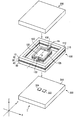
図1に、本発明の実施の形態のマイクロミラー装置1の構成を分解斜視図で示す。また、図2に、マイクロミラー装置1の構成を切断面図で示す。なお、説明の便宜上、互いに直交するX、Y、Z軸を図1および2に付す。図2について説明を加えると、当該切断面図は、図1の軸Axを含むYZ平面でマイクロミラー装置1を切断して示した図となっている。 FIG. 1 is an exploded perspective view showing the configuration of a micromirror device 1 according to an embodiment of the present invention. FIG. 2 is a sectional view showing the configuration of the micromirror device 1. For convenience of explanation, the X, Y, and Z axes orthogonal to each other are attached to FIGS. Referring to FIG. 2, the cut surface view is a view showing the micromirror device 1 cut along a YZ plane including the axis Ax in FIG. 1.
マイクロミラー装置1は、例えばバーコードリーダやレーザプリンタ等の種々の機器に実装され、機器内部の支持基板(不図示)上に支持される。マイクロミラー装置1は、マイクロミラーデバイス部100、蓋部200および下部基板300を備える。
The micromirror device 1 is mounted on various devices such as a barcode reader and a laser printer, and is supported on a support substrate (not shown) inside the device. The micromirror device 1 includes a
マイクロミラーデバイス部100は、中空矩形に形成された枠部110を有する。枠部110の中空部分には、マイクロミラーデバイス部100の可動部分が形成される。可動部分は、ミラー部120および、軸Axを中心軸とした一対のトーションバー130を含む。各トーションバー130の一端は枠部110に支持され、他端はミラー部120を軸Ax周りに揺動可能に支持する。
The
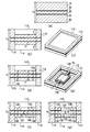
ここで、図3を参照して、マイクロミラーデバイス部100の製造プロセスについて説明する。マイクロミラーデバイス部100は、5層構造のウェハを用いて、以下の製造プロセスで形成される。
Here, with reference to FIG. 3, the manufacturing process of the
当該ウェハは、図3(a)に示されるように、単結晶シリコン層10、SiO2層20、単結晶シリコン層30、SiO2層40、単結晶シリコン層50を順に堆積させた層構造を有する。なお、図3は説明の便宜上、ウェハ全体でなく単一のダイについてのみ図示する。また、図3(a)、(b)、(d)、および(f)、(g)はウェハの断面図を示し、図3(c)および(e)はウェハの斜視図を示す。また、図3の製造プロセス前のウェハのZ軸方向の膜厚は図3(a)に示されるようにt0である。
As shown in FIG. 3A, the wafer has a layer structure in which a single
図3の製造プロセスによれば、先ず、図3(a)のウェハに対して、例えば熱酸化によるSiO2膜の形成、当該SiO2膜のパターニング等が施され、単結晶シリコン層10上にマスクパターンが形成される。このマスクパターンは、図1および2に示される枠部110の上面112に対応する領域に形成される。次いで、例えばKOH(水酸化カリウム)等を用いてエッチング処理が施され、マスクパターンから露出した領域に対応する部分(以下、「中空領域部分」という)の単結晶シリコン層10が所定の深さtまで除去される。
According to the manufacturing process of FIG. 3, first, for example, formation of a SiO 2 film by thermal oxidation, patterning of the SiO 2 film, etc. are performed on the wafer of FIG. 3A, and a mask pattern is formed on the single
単結晶シリコン層10に施した上記一連の処理(SiO2膜形成、パターニング、およびエッチング)がウェハの裏面、つまり単結晶シリコン層50に対しても施される。単結晶シリコン層50上のマスクパターンは、図2に示される枠部110の下面114に対応する領域に形成される。
The above-described series of processing (SiO 2 film formation, patterning, and etching) applied to the single
単結晶シリコン層10と単結晶シリコン層50の双方に上記一連の処理を施すことにより、ウェハは図3(b)および(c)の状態となる。すなわち、中空領域部分がエッチング処理で除去され、当該中空領域部分に対応するウェハの膜厚がt1となる。なお、除去深さtはSiO2層20、40を露出させない程度の深さである。この工程でのエッチング処理における除去深さは、エッチングの時間を管理することでコントロール可能である。また、図面の簡略化のため、図3の各図においてマスクパターンの図示は省略する。
By performing the above-described series of processes on both the single
次に、中空領域部分のうち、ミラー部120および一対のトーションバー130に対応する領域(以下、「可動部分領域」という)にマスクパターンが形成される。そして、単結晶シリコン層向けのエッチング処理(例えばKOHを用いたエッチング処理)、SiO2層向けのエッチング処理(例えば反応性イオンエッチング(RIE))が順次施され、中空領域部分のうち、可動部分領域以外の領域の5層全てが除去される(図3(d)および(e)参照)。
Next, a mask pattern is formed in a region corresponding to the
更に、可動部分領域のうち、図1、図2に示されるミラー面122、ミラー裏面124に対応する領域のマスクパターンが除去されて、マスクパターン除去領域に対してKOH等によるエッチング処理が施される。ここで、SiO2層20および40はエッチストップ層として機能する。よって、当該除去領域の膜厚は図3(f)に示されるように、SiO2層20−SiO2層40間の層厚t2となる。
Further, in the movable part region, the mask pattern of the region corresponding to the
次いで、RIE等により上記マスクパターン除去領域上のSiO2層20および40が除去されて、該除去後の領域にメタライズ等によって金属膜が形成される。なお、図面の簡略化のため、各図面において金属膜の図示を省略する。また、金属膜形成後のSiO2層20側の面を「ミラー面122」、SiO2層40側の面を「ミラー裏面124」と記す。
Next, the SiO2 layers 20 and 40 on the mask pattern removal region are removed by RIE or the like, and a metal film is formed in the region after the removal by metallization or the like. For simplification of the drawings, illustration of the metal film is omitted in each drawing. Further, the surface on the SiO 2
ミラー面122−ミラー裏面124間の膜厚t3は、SiO2層20および40のエッチストップにより、単結晶シリコン層30およびその両面の金属膜の膜厚で精密に規定される。また、当該エッチストップにより、ミラー面122−ミラー裏面124間は優れた膜厚均一性を得られる。このためミラー面122−ミラー裏面124間の膜厚を薄肉に形成した場合であっても、ダイの歩留まりは比較的安定する。
The film thickness t3 between the
次いで、全てのマスクパターンが除去されると図3の製造プロセスが終了し、ウェハは図3(g)および図1に示される状態になる。すなわちウェハは、各ダイが、枠部110と、その中空部分にミラー部120および一対のトーションバー130を有した形状に形成される。また、ミラー部120には、可動部分領域中の上記マスクパターン除去領域に対するエッチング処理によってミラー面122やミラー裏面124よりも突出した形状であるリブ126が形成される。
Next, when all the mask patterns are removed, the manufacturing process of FIG. 3 is completed, and the wafer is in the state shown in FIG. 3G and FIG. That is, the wafer is formed in a shape in which each die has a
ミラー面122−ミラー裏面124間の膜厚t3は非常に薄い。よって、例えばミラー部120全体の膜厚がt3である場合、ミラー部120の強度や剛性が実用上問題(例えば割れや破断、変形等)を生じ得る程度に低下する恐れがある。本実施形態では、このような問題発生を防止するため、上記製造プロセスでミラー面122の周辺部にリブ126を形成する構成を採用している。すなわち本実施形態によれば、ミラー部120の中央部を薄肉形成してミラー部120を軽量化すると共に、ミラー部120の全周にリブ126を形成してミラー部120全体の強度および剛性の確保も達成している。
The film thickness t3 between the
次に、図1および2を用いた説明に戻る。以降の説明では、マイクロミラー装置1の構成を更に説明しつつ可動部分の動作についても併せて説明する。 Next, the description returns to FIGS. 1 and 2. In the following description, the operation of the movable part is also described while further explaining the configuration of the micromirror device 1.
図2に示されるように、枠部110の上面112、下面114はそれぞれ蓋部200、下部基板300に接合される。蓋部200はガラス基板、下部基板300は例えば枠部110と同様にシリコン基板で形成されており、例えば陽極接合によって接合される。このとき陽極接合によって各接合部分は強固な結合力で結合する。
As shown in FIG. 2, the
また、枠部110は図3の製造プロセスにあるように、ウェハ上で除去されない部分であり、ミラー部120およびトーションバー130(膜厚t1、t3)よりも厚みを有する(膜厚t0)。そして、ミラー部120およびトーションバー130を四側面から覆うよう矩形に形成されている。よって、ミラー部120およびトーションバー130は、上記接合処理で枠部110の上面、下面それぞれに蓋部200、下部基板300が接合されると、図2に示されるように、枠部110、蓋部200、および下部基板300で形成されるキャビティに収容された状態となる。
Further, as in the manufacturing process of FIG. 3, the
また、膜厚t0は、ミラー部120の可動範囲がキャビティに完全に収まるように設計されている。よって、本実施形態によれば、マイクロミラーデバイス部100−蓋部200間、およびマイクロミラーデバイス部100−下部基板300間にスペーサ等の別個の構成要素を介在させることなくキャビティを形成することが可能となる。これには、スペーサ等の別個の構成要素とマイクロミラーデバイス部100との接合や当該接合のためのアライメント等の工程を削減するメリットがある。
Further, the film thickness t0 is designed so that the movable range of the
なお、キャビティの雰囲気は真空とすることが望ましい。キャビティの雰囲気を真空とすることで、例えばミラー部120が可動した際に受ける空気の粘性抵抗を考慮する必要がない、ミラー部120のQ値が安定する等の、マイクロミラー装置1の性能を安定させられる効果が得られるためである。
Note that the atmosphere of the cavity is preferably a vacuum. By making the atmosphere of the cavity a vacuum, for example, it is not necessary to consider the viscous resistance of the air received when the
蓋部200は光透過部材で形成されており、ミラー部120に対するレーザ光の入出射窓として機能する。このレーザ光は被走査物上を走査するための光であり、図示しない光源から射出される。蓋部200を透過したレーザ光はミラー面122に入射して、当該ミラー面122の傾き角に応じた方向に反射する。反射光は蓋部200を再び透過して射出し、マイクロミラー装置1からの走査光として被走査物上を走査する。
The
下部基板300の上面310には軸Axを含むYZ平面を挟み、電極322、324が対向離間して配置される。電極322、324はそれぞれスルーホール332、334を介して、上面310の裏面から引き出される配線(不図示)と電気的に接続される。また、マイクロミラーデバイス部100のミラー部120(単結晶シリコン層30)からも配線が引き出される。これらの配線は、マイクロミラー装置1を駆動制御する駆動制御回路(不図示)と接続される。なお、単結晶シリコン層30は、SiO2層20および40により他の層と絶縁されている。
On the
上記駆動制御回路がミラー部120と各電極間で非対称な電位差を生じさせるよう電圧を印加すると、ミラー部120が軸Ax周りに傾く。例えば上記駆動制御回路がミラー部120および電極324をグランド、ミラー裏面124−電極322間に電位差Vが生じるよう駆動制御した場合、ミラー部120は、ミラー裏面124−電極322間で発生した静電引力によって軸Ax周りの力のモーメントを受けて、軸Ax周りを図1の矢印R方向に回転するように傾く。また、例えば上記駆動制御回路がミラー部120および電極322をグランド、ミラー裏面124−電極324間に電位差Vが生じるよう駆動制御した場合、ミラー部120は上記と同様の作用によって軸Ax周りを矢印R方向と逆方向に回転するように傾く。この2パターンの電圧印加を交互に繰り返すことでミラー部120は振動し、走査光を被走査物上で走査することが可能となる。
When the drive control circuit applies a voltage so as to generate an asymmetric potential difference between the
すなわち本実施形態によれば、ミラー部120の中央部を薄肉形成して且つ周辺部を中央部よりも一段高く形成することで、ミラー部120全体を軽量化すると共に、実用上必要とされる強度および剛性を確保することが可能となる。また、リブ126を形成することでミラー部120の共振周波数を上げる効果も期待される。
That is, according to the present embodiment, the center part of the
以上が本発明の実施の形態である。本発明はこれらの実施の形態に限定されるものではなく様々な範囲で変形が可能である。例えばリブ126の形状や形成位置等には種々のパターンが想定される。例えば本実施形態ではリブ126をミラー部120の全周に形成しているが、別の実施の形態ではミラー部120周辺部の一部分(例えばトーションバー130が形成されているミラー部120上の辺)にだけ形成しても良い。また、リブ126をミラー面122およびミラー裏面124の両面でなく片面だけに形成しても良い。
The above is the embodiment of the present invention. The present invention is not limited to these embodiments and can be modified in various ranges. For example, various patterns are assumed for the shape and formation position of the
また、本実施形態ではミラー部120およびミラー面122は矩形状であるが、別の実施形態では他の形状(例えば円状や楕円状等)であっても良い。ミラー面122に関しては、少なくとも光学素子面として利用する有効領域がエッチストップ等で高い面精度を有していればその機能は十分に果たされる。
In the present embodiment, the
また、本実施形態では一軸のマイクロミラー装置について説明したが、本実施形態のミラー部120と同様の構成は、二軸或いはより多軸のマイクロミラー装置のミラー部に対しても適用可能である。
Further, although the uniaxial micromirror device has been described in the present embodiment, the same configuration as that of the
また、ウェハは、SiO2層を有さない1層の単結晶シリコン層であっても良く、或いは2層の単結晶シリコン層間にSiO2層を介在させたもの(以下、「SOI基板」という)であっても良い。すなわち単結晶シリコン層のエッチング時間を精密に管理すれば、ミラー部120の膜厚を精密に規定でき、また、ミラー面122やミラー裏面124の面精度を高くすることも可能である。よって、ウェハが1層の単結晶シリコン層であってもSOI基板であっても本実施形態のマイクロミラー装置1と同等のものを製造することが可能である。
In addition, the wafer may be a single monocrystalline silicon layer that does not have an SiO2 layer, or an SiO2 layer interposed between two monocrystalline silicon layers (hereinafter referred to as “SOI substrate”). There may be. That is, if the etching time of the single crystal silicon layer is precisely managed, the film thickness of the
また、本発明は、本実施形態の平面平板型のマイクロミラー装置に限らず、櫛歯型の静電駆動ミラー、或いは他の駆動方式のミラーにも適用可能である。 The present invention is not limited to the flat plate type micromirror device of the present embodiment, but can be applied to a comb-shaped electrostatic drive mirror or a mirror of another drive system.
1 マイクロミラー装置
100 マイクロミラーデバイス部
110 枠部
120 ミラー部
122 ミラー面
124 ミラー裏面
126 リブ
130 トーションバー
200 蓋部
300 下部基板
DESCRIPTION OF SYMBOLS 1
Claims (5)
光源からの光を走査光として反射するミラー部を備え、
前記ミラー部の中央部の膜厚が当該ミラー部の周辺部の膜厚よりも薄くなるよう形成されたこと、を特徴とするマイクロミラー装置。 In a micromirror device that scans light,
A mirror unit that reflects light from the light source as scanning light;
A micromirror device characterized by being formed so that the film thickness of the central part of the mirror part is thinner than the film thickness of the peripheral part of the mirror part.
該基台表面の所定領域に第1のマスクパターンを形成する第1のマスクパターン形成ステップと、
前記第1のマスクパターンから露出した領域を除去して前記ミラー部に対応したミラー形状を形成するミラー形状形成ステップと、
前記ミラー形状に対応する領域のうち当該ミラー形状の周辺領域のみに第2のマスクパターンを形成する第2のマスクパターン形成ステップと、
前記第2のマスクパターンから露出した前記ミラー形状の中央領域を所定の深さだけ除去して、当該中央領域の膜厚を該ミラー形状の周辺領域の膜厚よりも薄肉に形成する薄肉形成ステップと、を含むミラー部形成方法。 In a mirror part forming method for forming a mirror part supported to be swingable with respect to a base,
A first mask pattern forming step for forming a first mask pattern in a predetermined region on the surface of the base;
A mirror shape forming step of removing a region exposed from the first mask pattern to form a mirror shape corresponding to the mirror portion;
A second mask pattern forming step of forming a second mask pattern only in a peripheral region of the mirror shape among regions corresponding to the mirror shape;
A thin-wall forming step of removing the mirror-shaped central region exposed from the second mask pattern by a predetermined depth and forming the film thickness of the central region to be thinner than the film thickness of the peripheral region of the mirror shape And a mirror part forming method.
前記薄肉形成ステップにおいて、該中央領域の膜厚がエッチストップ層で規定される、ミラー部形成方法。 The base includes an etch stop layer;
The method for forming a mirror part, wherein in the thin-wall forming step, the film thickness of the central region is defined by an etch stop layer.
Priority Applications (1)
| Application Number | Priority Date | Filing Date | Title |
|---|---|---|---|
| JP2007266190A JP2009093105A (en) | 2007-10-12 | 2007-10-12 | Micromirror device, and mirror part forming method |
Applications Claiming Priority (1)
| Application Number | Priority Date | Filing Date | Title |
|---|---|---|---|
| JP2007266190A JP2009093105A (en) | 2007-10-12 | 2007-10-12 | Micromirror device, and mirror part forming method |
Publications (1)
| Publication Number | Publication Date |
|---|---|
| JP2009093105A true JP2009093105A (en) | 2009-04-30 |
Family
ID=40665123
Family Applications (1)
| Application Number | Title | Priority Date | Filing Date |
|---|---|---|---|
| JP2007266190A Withdrawn JP2009093105A (en) | 2007-10-12 | 2007-10-12 | Micromirror device, and mirror part forming method |
Country Status (1)
| Country | Link |
|---|---|
| JP (1) | JP2009093105A (en) |
Cited By (8)
| Publication number | Priority date | Publication date | Assignee | Title |
|---|---|---|---|---|
| JP2010128116A (en) * | 2008-11-27 | 2010-06-10 | Ricoh Co Ltd | Optical scanner |
| JP2011087421A (en) * | 2009-10-16 | 2011-04-28 | Nippon Signal Co Ltd:The | Planar type actuator and method for manufacturing the same |
| JP2014059527A (en) * | 2012-09-19 | 2014-04-03 | Stanley Electric Co Ltd | Method for manufacturing optical deflector |
| JP2016018029A (en) * | 2014-07-07 | 2016-02-01 | 株式会社Jvcケンウッド | Optical deflector |
| JP2020129116A (en) * | 2017-07-06 | 2020-08-27 | 浜松ホトニクス株式会社 | Optical device |
| CN113135547A (en) * | 2021-03-10 | 2021-07-20 | 苏州深水渔半导体有限公司 | Optical chip and method for producing the same |
| CN114730073A (en) * | 2019-11-21 | 2022-07-08 | 浜松光子学株式会社 | Mirror assembly |
| CN113135547B (en) * | 2021-03-10 | 2024-04-19 | 苏州深水渔半导体有限公司 | Method for producing optical chip |
Citations (5)
| Publication number | Priority date | Publication date | Assignee | Title |
|---|---|---|---|---|
| JPH11305162A (en) * | 1998-04-27 | 1999-11-05 | Olympus Optical Co Ltd | Optical scanner |
| JP2003315724A (en) * | 2002-04-26 | 2003-11-06 | Ricoh Co Ltd | Vibrating mirror and method for manufacturing the same, optical scanner, and image forming device |
| JP2004258158A (en) * | 2003-02-25 | 2004-09-16 | Miyota Kk | Planer type electromagnetic actuator |
| JP2006293176A (en) * | 2005-04-13 | 2006-10-26 | Sony Corp | Optical control element, method of manufacturing the same and display device |
| JP2007271787A (en) * | 2006-03-30 | 2007-10-18 | Brother Ind Ltd | Vibrating element, method of manufacturing vibrating element, optical scanner, image forming apparatus and image display device |
-
2007
- 2007-10-12 JP JP2007266190A patent/JP2009093105A/en not_active Withdrawn
Patent Citations (5)
| Publication number | Priority date | Publication date | Assignee | Title |
|---|---|---|---|---|
| JPH11305162A (en) * | 1998-04-27 | 1999-11-05 | Olympus Optical Co Ltd | Optical scanner |
| JP2003315724A (en) * | 2002-04-26 | 2003-11-06 | Ricoh Co Ltd | Vibrating mirror and method for manufacturing the same, optical scanner, and image forming device |
| JP2004258158A (en) * | 2003-02-25 | 2004-09-16 | Miyota Kk | Planer type electromagnetic actuator |
| JP2006293176A (en) * | 2005-04-13 | 2006-10-26 | Sony Corp | Optical control element, method of manufacturing the same and display device |
| JP2007271787A (en) * | 2006-03-30 | 2007-10-18 | Brother Ind Ltd | Vibrating element, method of manufacturing vibrating element, optical scanner, image forming apparatus and image display device |
Cited By (14)
| Publication number | Priority date | Publication date | Assignee | Title |
|---|---|---|---|---|
| JP2010128116A (en) * | 2008-11-27 | 2010-06-10 | Ricoh Co Ltd | Optical scanner |
| JP2011087421A (en) * | 2009-10-16 | 2011-04-28 | Nippon Signal Co Ltd:The | Planar type actuator and method for manufacturing the same |
| JP2014059527A (en) * | 2012-09-19 | 2014-04-03 | Stanley Electric Co Ltd | Method for manufacturing optical deflector |
| JP2016018029A (en) * | 2014-07-07 | 2016-02-01 | 株式会社Jvcケンウッド | Optical deflector |
| US11629947B2 (en) | 2017-07-06 | 2023-04-18 | Hamamatsu Photonics K.K. | Optical device |
| JP7153685B2 (en) | 2017-07-06 | 2022-10-14 | 浜松ホトニクス株式会社 | optical device |
| US11624605B2 (en) | 2017-07-06 | 2023-04-11 | Hamamatsu Photonics K.K. | Mirror unit and optical module |
| JP2020129116A (en) * | 2017-07-06 | 2020-08-27 | 浜松ホトニクス株式会社 | Optical device |
| US11629946B2 (en) | 2017-07-06 | 2023-04-18 | Hamamatsu Photonics K.K. | Mirror unit and optical module |
| US11635290B2 (en) | 2017-07-06 | 2023-04-25 | Hamamatsu Photonics K.K. | Optical module |
| US11879731B2 (en) | 2017-07-06 | 2024-01-23 | Hamamatsu Photonics K.K. | Mirror unit and optical module |
| CN114730073A (en) * | 2019-11-21 | 2022-07-08 | 浜松光子学株式会社 | Mirror assembly |
| CN113135547A (en) * | 2021-03-10 | 2021-07-20 | 苏州深水渔半导体有限公司 | Optical chip and method for producing the same |
| CN113135547B (en) * | 2021-03-10 | 2024-04-19 | 苏州深水渔半导体有限公司 | Method for producing optical chip |
Similar Documents
| Publication | Publication Date | Title |
|---|---|---|
| KR101306847B1 (en) | Optical scanning device | |
| KR101090961B1 (en) | The optical scanner and manufacturing method thereof | |
| JP5876329B2 (en) | Manufacturing method of optical scanner | |
| JP2009093105A (en) | Micromirror device, and mirror part forming method | |
| JP2003172897A (en) | Optical scanner and its manufacturing method, optical writing device, image forming apparatus, vibratory mirror chip and its manufacturing method, and optical scanning module | |
| US20050184351A1 (en) | Mems scanning mirror with trenched surface and tapered comb teeth for reducing inertia and deformation | |
| JP4351586B2 (en) | Optical scanner having curved mirror and method for manufacturing the same | |
| JP4151959B2 (en) | Vibrating mirror and manufacturing method thereof, optical writing device, and image forming apparatus | |
| JP2003005101A (en) | Optical modulation device and method for manufacturing the same | |
| JP2005266566A (en) | Polarizing mirror, method for manufacturing the polarizing mirror, optical writer, and image forming apparatus | |
| JPH10104543A (en) | Optical scanning device and method therefor | |
| JP3910333B2 (en) | Galvano micromirror and manufacturing method thereof | |
| US20100302609A1 (en) | Mems device having reduced deformations | |
| JP2009122155A (en) | Micro-device manufacturing method and micro--device | |
| JP2009098253A (en) | Optical reflection element and image projector using the same | |
| JP2012163792A (en) | Optical scanning element and image display device | |
| JP2005279863A (en) | Manufacturing method of actuator and actuator | |
| JP4835024B2 (en) | Light control element, manufacturing method thereof, and display device | |
| JP7193719B2 (en) | optical scanner | |
| JPH0933828A (en) | Scanning microelement for optical system | |
| US7046421B1 (en) | MEMS scanning mirror with trenched surface and I-beam like cross-section for reducing inertia and deformation | |
| JP2007171780A (en) | Drive device and manufacturing method therefor, and display apparatus | |
| JP2017068213A (en) | Optical scanner, method for manufacturing optical scanner, image display device and head mount display | |
| JP2014048327A (en) | Light deflector, image display device using the same, and method for manufacturing light deflector | |
| JP5077139B2 (en) | Optical reflection element |
Legal Events
| Date | Code | Title | Description |
|---|---|---|---|
| A621 | Written request for application examination |
Free format text: JAPANESE INTERMEDIATE CODE: A621 Effective date: 20100726 |
|
| A711 | Notification of change in applicant |
Free format text: JAPANESE INTERMEDIATE CODE: A712 Effective date: 20111202 |
|
| A977 | Report on retrieval |
Free format text: JAPANESE INTERMEDIATE CODE: A971007 Effective date: 20111227 |
|
| A131 | Notification of reasons for refusal |
Free format text: JAPANESE INTERMEDIATE CODE: A131 Effective date: 20120118 |
|
| A761 | Written withdrawal of application |
Free format text: JAPANESE INTERMEDIATE CODE: A761 Effective date: 20120306 |