JP2009031392A - ワイヤーグリッド型偏光素子、その製造方法、液晶装置および投射型表示装置 - Google Patents
ワイヤーグリッド型偏光素子、その製造方法、液晶装置および投射型表示装置 Download PDFInfo
- Publication number
- JP2009031392A JP2009031392A JP2007192990A JP2007192990A JP2009031392A JP 2009031392 A JP2009031392 A JP 2009031392A JP 2007192990 A JP2007192990 A JP 2007192990A JP 2007192990 A JP2007192990 A JP 2007192990A JP 2009031392 A JP2009031392 A JP 2009031392A
- Authority
- JP
- Japan
- Prior art keywords
- polarizing element
- wire grid
- metal
- grid type
- substrate surface
- Prior art date
- Legal status (The legal status is an assumption and is not a legal conclusion. Google has not performed a legal analysis and makes no representation as to the accuracy of the status listed.)
- Withdrawn
Links
- 239000004973 liquid crystal related substance Substances 0.000 title claims abstract description 56
- 238000004519 manufacturing process Methods 0.000 title claims abstract description 22
- 239000000758 substrate Substances 0.000 claims abstract description 136
- 229910052751 metal Inorganic materials 0.000 claims abstract description 126
- 239000002184 metal Substances 0.000 claims abstract description 126
- 238000002834 transmittance Methods 0.000 claims abstract description 25
- 238000005530 etching Methods 0.000 claims description 39
- 239000010410 layer Substances 0.000 claims description 20
- 230000010287 polarization Effects 0.000 claims description 18
- 238000005498 polishing Methods 0.000 claims description 17
- 230000003287 optical effect Effects 0.000 claims description 13
- 239000011241 protective layer Substances 0.000 claims description 13
- 239000000463 material Substances 0.000 claims description 12
- 239000011347 resin Substances 0.000 claims description 10
- 229920005989 resin Polymers 0.000 claims description 10
- 238000007517 polishing process Methods 0.000 claims description 6
- 239000000126 substance Substances 0.000 claims description 6
- 238000000465 moulding Methods 0.000 claims description 2
- 238000000227 grinding Methods 0.000 claims 1
- 238000000034 method Methods 0.000 abstract description 12
- VYPSYNLAJGMNEJ-UHFFFAOYSA-N Silicium dioxide Chemical compound O=[Si]=O VYPSYNLAJGMNEJ-UHFFFAOYSA-N 0.000 abstract description 8
- 239000011521 glass Substances 0.000 abstract description 5
- XEEYBQQBJWHFJM-UHFFFAOYSA-N Iron Chemical compound [Fe] XEEYBQQBJWHFJM-UHFFFAOYSA-N 0.000 description 6
- PXHVJJICTQNCMI-UHFFFAOYSA-N Nickel Chemical compound [Ni] PXHVJJICTQNCMI-UHFFFAOYSA-N 0.000 description 6
- KDLHZDBZIXYQEI-UHFFFAOYSA-N Palladium Chemical compound [Pd] KDLHZDBZIXYQEI-UHFFFAOYSA-N 0.000 description 6
- BASFCYQUMIYNBI-UHFFFAOYSA-N platinum Chemical compound [Pt] BASFCYQUMIYNBI-UHFFFAOYSA-N 0.000 description 6
- 230000008569 process Effects 0.000 description 6
- 229910052814 silicon oxide Inorganic materials 0.000 description 5
- 229910052581 Si3N4 Inorganic materials 0.000 description 4
- 230000015572 biosynthetic process Effects 0.000 description 4
- 229910044991 metal oxide Inorganic materials 0.000 description 4
- 150000004706 metal oxides Chemical class 0.000 description 4
- 150000004767 nitrides Chemical class 0.000 description 4
- HQVNEWCFYHHQES-UHFFFAOYSA-N silicon nitride Chemical compound N12[Si]34N5[Si]62N3[Si]51N64 HQVNEWCFYHHQES-UHFFFAOYSA-N 0.000 description 4
- VYZAMTAEIAYCRO-UHFFFAOYSA-N Chromium Chemical compound [Cr] VYZAMTAEIAYCRO-UHFFFAOYSA-N 0.000 description 3
- RYGMFSIKBFXOCR-UHFFFAOYSA-N Copper Chemical compound [Cu] RYGMFSIKBFXOCR-UHFFFAOYSA-N 0.000 description 3
- ZOKXTWBITQBERF-UHFFFAOYSA-N Molybdenum Chemical compound [Mo] ZOKXTWBITQBERF-UHFFFAOYSA-N 0.000 description 3
- 229910052779 Neodymium Inorganic materials 0.000 description 3
- KJTLSVCANCCWHF-UHFFFAOYSA-N Ruthenium Chemical compound [Ru] KJTLSVCANCCWHF-UHFFFAOYSA-N 0.000 description 3
- XUIMIQQOPSSXEZ-UHFFFAOYSA-N Silicon Chemical compound [Si] XUIMIQQOPSSXEZ-UHFFFAOYSA-N 0.000 description 3
- BQCADISMDOOEFD-UHFFFAOYSA-N Silver Chemical compound [Ag] BQCADISMDOOEFD-UHFFFAOYSA-N 0.000 description 3
- RTAQQCXQSZGOHL-UHFFFAOYSA-N Titanium Chemical compound [Ti] RTAQQCXQSZGOHL-UHFFFAOYSA-N 0.000 description 3
- 229910052769 Ytterbium Inorganic materials 0.000 description 3
- 229910052782 aluminium Inorganic materials 0.000 description 3
- XAGFODPZIPBFFR-UHFFFAOYSA-N aluminium Chemical compound [Al] XAGFODPZIPBFFR-UHFFFAOYSA-N 0.000 description 3
- 229910052797 bismuth Inorganic materials 0.000 description 3
- JCXGWMGPZLAOME-UHFFFAOYSA-N bismuth atom Chemical compound [Bi] JCXGWMGPZLAOME-UHFFFAOYSA-N 0.000 description 3
- 238000006243 chemical reaction Methods 0.000 description 3
- 229910052804 chromium Inorganic materials 0.000 description 3
- 239000011651 chromium Substances 0.000 description 3
- 229910017052 cobalt Inorganic materials 0.000 description 3
- 239000010941 cobalt Substances 0.000 description 3
- GUTLYIVDDKVIGB-UHFFFAOYSA-N cobalt atom Chemical compound [Co] GUTLYIVDDKVIGB-UHFFFAOYSA-N 0.000 description 3
- 229910052802 copper Inorganic materials 0.000 description 3
- 239000010949 copper Substances 0.000 description 3
- PCHJSUWPFVWCPO-UHFFFAOYSA-N gold Chemical compound [Au] PCHJSUWPFVWCPO-UHFFFAOYSA-N 0.000 description 3
- 229910052737 gold Inorganic materials 0.000 description 3
- 239000010931 gold Substances 0.000 description 3
- 229910052738 indium Inorganic materials 0.000 description 3
- APFVFJFRJDLVQX-UHFFFAOYSA-N indium atom Chemical compound [In] APFVFJFRJDLVQX-UHFFFAOYSA-N 0.000 description 3
- 229910052742 iron Inorganic materials 0.000 description 3
- WPBNNNQJVZRUHP-UHFFFAOYSA-L manganese(2+);methyl n-[[2-(methoxycarbonylcarbamothioylamino)phenyl]carbamothioyl]carbamate;n-[2-(sulfidocarbothioylamino)ethyl]carbamodithioate Chemical compound [Mn+2].[S-]C(=S)NCCNC([S-])=S.COC(=O)NC(=S)NC1=CC=CC=C1NC(=S)NC(=O)OC WPBNNNQJVZRUHP-UHFFFAOYSA-L 0.000 description 3
- 229910052750 molybdenum Inorganic materials 0.000 description 3
- 239000011733 molybdenum Substances 0.000 description 3
- QEFYFXOXNSNQGX-UHFFFAOYSA-N neodymium atom Chemical compound [Nd] QEFYFXOXNSNQGX-UHFFFAOYSA-N 0.000 description 3
- 229910052759 nickel Inorganic materials 0.000 description 3
- 229910052758 niobium Inorganic materials 0.000 description 3
- 239000010955 niobium Substances 0.000 description 3
- GUCVJGMIXFAOAE-UHFFFAOYSA-N niobium atom Chemical compound [Nb] GUCVJGMIXFAOAE-UHFFFAOYSA-N 0.000 description 3
- 229910052763 palladium Inorganic materials 0.000 description 3
- 230000035699 permeability Effects 0.000 description 3
- 229910052697 platinum Inorganic materials 0.000 description 3
- 229910052703 rhodium Inorganic materials 0.000 description 3
- 239000010948 rhodium Substances 0.000 description 3
- MHOVAHRLVXNVSD-UHFFFAOYSA-N rhodium atom Chemical compound [Rh] MHOVAHRLVXNVSD-UHFFFAOYSA-N 0.000 description 3
- 229910052707 ruthenium Inorganic materials 0.000 description 3
- 229910052710 silicon Inorganic materials 0.000 description 3
- 239000010703 silicon Substances 0.000 description 3
- 229910052709 silver Inorganic materials 0.000 description 3
- 239000004332 silver Substances 0.000 description 3
- 239000002356 single layer Substances 0.000 description 3
- 239000010936 titanium Substances 0.000 description 3
- 229910052719 titanium Inorganic materials 0.000 description 3
- WFKWXMTUELFFGS-UHFFFAOYSA-N tungsten Chemical compound [W] WFKWXMTUELFFGS-UHFFFAOYSA-N 0.000 description 3
- 229910052721 tungsten Inorganic materials 0.000 description 3
- 239000010937 tungsten Substances 0.000 description 3
- NAWDYIZEMPQZHO-UHFFFAOYSA-N ytterbium Chemical compound [Yb] NAWDYIZEMPQZHO-UHFFFAOYSA-N 0.000 description 3
- 229910052727 yttrium Inorganic materials 0.000 description 3
- VWQVUPCCIRVNHF-UHFFFAOYSA-N yttrium atom Chemical compound [Y] VWQVUPCCIRVNHF-UHFFFAOYSA-N 0.000 description 3
- PXGOKWXKJXAPGV-UHFFFAOYSA-N Fluorine Chemical compound FF PXGOKWXKJXAPGV-UHFFFAOYSA-N 0.000 description 2
- 239000000956 alloy Substances 0.000 description 2
- 229910045601 alloy Inorganic materials 0.000 description 2
- QVGXLLKOCUKJST-UHFFFAOYSA-N atomic oxygen Chemical compound [O] QVGXLLKOCUKJST-UHFFFAOYSA-N 0.000 description 2
- 230000008859 change Effects 0.000 description 2
- 238000005229 chemical vapour deposition Methods 0.000 description 2
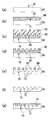
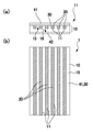
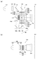
- 238000010586 diagram Methods 0.000 description 2
- 238000001312 dry etching Methods 0.000 description 2
- 238000010894 electron beam technology Methods 0.000 description 2
- 239000004744 fabric Substances 0.000 description 2
- 239000011737 fluorine Substances 0.000 description 2
- 229910052731 fluorine Inorganic materials 0.000 description 2
- 239000007789 gas Substances 0.000 description 2
- 239000001301 oxygen Substances 0.000 description 2
- 229910052760 oxygen Inorganic materials 0.000 description 2
- 239000002245 particle Substances 0.000 description 2
- 238000003825 pressing Methods 0.000 description 2
- 229920005830 Polyurethane Foam Polymers 0.000 description 1
- GWEVSGVZZGPLCZ-UHFFFAOYSA-N Titan oxide Chemical compound O=[Ti]=O GWEVSGVZZGPLCZ-UHFFFAOYSA-N 0.000 description 1
- 150000001252 acrylic acid derivatives Chemical class 0.000 description 1
- 230000009471 action Effects 0.000 description 1
- 230000008901 benefit Effects 0.000 description 1
- 229910000420 cerium oxide Inorganic materials 0.000 description 1
- 238000007796 conventional method Methods 0.000 description 1
- 230000003247 decreasing effect Effects 0.000 description 1
- 239000002270 dispersing agent Substances 0.000 description 1
- 238000009826 distribution Methods 0.000 description 1
- 230000000694 effects Effects 0.000 description 1
- 230000020169 heat generation Effects 0.000 description 1
- 238000010438 heat treatment Methods 0.000 description 1
- 230000001678 irradiating effect Effects 0.000 description 1
- 239000007788 liquid Substances 0.000 description 1
- QSHDDOUJBYECFT-UHFFFAOYSA-N mercury Chemical compound [Hg] QSHDDOUJBYECFT-UHFFFAOYSA-N 0.000 description 1
- 229910052753 mercury Inorganic materials 0.000 description 1
- 150000002739 metals Chemical class 0.000 description 1
- 239000004745 nonwoven fabric Substances 0.000 description 1
- BMMGVYCKOGBVEV-UHFFFAOYSA-N oxo(oxoceriooxy)cerium Chemical compound [Ce]=O.O=[Ce]=O BMMGVYCKOGBVEV-UHFFFAOYSA-N 0.000 description 1
- 238000001020 plasma etching Methods 0.000 description 1
- 239000011496 polyurethane foam Substances 0.000 description 1
- 238000000926 separation method Methods 0.000 description 1
- 238000004544 sputter deposition Methods 0.000 description 1
- 229920001187 thermosetting polymer Polymers 0.000 description 1
- OGIDPMRJRNCKJF-UHFFFAOYSA-N titanium oxide Inorganic materials [Ti]=O OGIDPMRJRNCKJF-UHFFFAOYSA-N 0.000 description 1
- 238000001771 vacuum deposition Methods 0.000 description 1
- XLYOFNOQVPJJNP-UHFFFAOYSA-N water Substances O XLYOFNOQVPJJNP-UHFFFAOYSA-N 0.000 description 1
Images


Classifications
-
- G—PHYSICS
- G02—OPTICS
- G02B—OPTICAL ELEMENTS, SYSTEMS OR APPARATUS
- G02B5/00—Optical elements other than lenses
- G02B5/30—Polarising elements
-
- G—PHYSICS
- G02—OPTICS
- G02B—OPTICAL ELEMENTS, SYSTEMS OR APPARATUS
- G02B5/00—Optical elements other than lenses
- G02B5/30—Polarising elements
- G02B5/3025—Polarisers, i.e. arrangements capable of producing a definite output polarisation state from an unpolarised input state
- G02B5/3058—Polarisers, i.e. arrangements capable of producing a definite output polarisation state from an unpolarised input state comprising electrically conductive elements, e.g. wire grids, conductive particles
-
- G—PHYSICS
- G02—OPTICS
- G02B—OPTICAL ELEMENTS, SYSTEMS OR APPARATUS
- G02B5/00—Optical elements other than lenses
- G02B5/18—Diffraction gratings
Landscapes
- Physics & Mathematics (AREA)
- General Physics & Mathematics (AREA)
- Optics & Photonics (AREA)
- Polarising Elements (AREA)
- Liquid Crystal (AREA)
- Projection Apparatus (AREA)
Priority Applications (4)
| Application Number | Priority Date | Filing Date | Title |
|---|---|---|---|
| JP2007192990A JP2009031392A (ja) | 2007-07-25 | 2007-07-25 | ワイヤーグリッド型偏光素子、その製造方法、液晶装置および投射型表示装置 |
| US12/145,229 US20090027773A1 (en) | 2007-07-25 | 2008-06-24 | Wire grid type polarization element, manufacturing method thereof, liquid crystal device, and projection type display apparatus |
| CNA2008101300313A CN101354458A (zh) | 2007-07-25 | 2008-07-24 | 线栅型偏振光元件及其制法、液晶装置及投射型显示装置 |
| KR1020080072001A KR20090012115A (ko) | 2007-07-25 | 2008-07-24 | 와이어 그리드형 편광 소자, 그 제조 방법, 액정 장치 및투사형 표시 장치 |
Applications Claiming Priority (1)
| Application Number | Priority Date | Filing Date | Title |
|---|---|---|---|
| JP2007192990A JP2009031392A (ja) | 2007-07-25 | 2007-07-25 | ワイヤーグリッド型偏光素子、その製造方法、液晶装置および投射型表示装置 |
Publications (2)
| Publication Number | Publication Date |
|---|---|
| JP2009031392A true JP2009031392A (ja) | 2009-02-12 |
| JP2009031392A5 JP2009031392A5 (enExample) | 2010-07-15 |
Family
ID=40295094
Family Applications (1)
| Application Number | Title | Priority Date | Filing Date |
|---|---|---|---|
| JP2007192990A Withdrawn JP2009031392A (ja) | 2007-07-25 | 2007-07-25 | ワイヤーグリッド型偏光素子、その製造方法、液晶装置および投射型表示装置 |
Country Status (4)
| Country | Link |
|---|---|
| US (1) | US20090027773A1 (enExample) |
| JP (1) | JP2009031392A (enExample) |
| KR (1) | KR20090012115A (enExample) |
| CN (1) | CN101354458A (enExample) |
Cited By (1)
| Publication number | Priority date | Publication date | Assignee | Title |
|---|---|---|---|---|
| JP2016153920A (ja) * | 2016-05-19 | 2016-08-25 | ウシオ電機株式会社 | 偏光光照射装置 |
Families Citing this family (33)
| Publication number | Priority date | Publication date | Assignee | Title |
|---|---|---|---|---|
| JP2010261999A (ja) * | 2009-04-30 | 2010-11-18 | Ricoh Co Ltd | 光学素子、偏光フィルタ、光アイソレータ、光学装置 |
| WO2011091556A1 (zh) * | 2010-01-26 | 2011-08-04 | Li Guanjun | 液晶屏与液晶显示装置 |
| JP5471674B2 (ja) * | 2010-03-23 | 2014-04-16 | セイコーエプソン株式会社 | プロジェクター |
| JP2011248284A (ja) * | 2010-05-31 | 2011-12-08 | Sony Chemical & Information Device Corp | 偏光板及び偏光板の製造方法 |
| US20130043956A1 (en) * | 2011-08-15 | 2013-02-21 | Honeywell International Inc. | Systems and methods for a nanofabricated optical circular polarizer |
| KR101856231B1 (ko) | 2011-12-19 | 2018-05-10 | 엘지이노텍 주식회사 | 나노패턴을 구비한 투명기판 및 그 제조방법 |
| WO2014196015A1 (ja) * | 2013-06-04 | 2014-12-11 | Necディスプレイソリューションズ株式会社 | 照明光学系及びプロジェクタ |
| CN104937448B (zh) * | 2013-09-06 | 2017-05-24 | 亚斯卡奈特股份有限公司 | 具备平行配置的光反射部的光控制面板的制造方法 |
| CN105511002B (zh) * | 2014-09-23 | 2018-03-20 | 中芯国际集成电路制造(上海)有限公司 | 一种光栅及其制造方法、电子装置 |
| JP6463934B2 (ja) * | 2014-09-29 | 2019-02-06 | Kyb株式会社 | サスペンション装置 |
| CN104297835B (zh) | 2014-10-17 | 2017-03-08 | 京东方科技集团股份有限公司 | 一种线栅偏振片的制作方法 |
| CN104347527B (zh) * | 2014-10-28 | 2017-02-15 | 北京思比科微电子技术股份有限公司 | 光学指纹传感器芯片封装玻璃光栅及其制作方法 |
| KR20160069048A (ko) * | 2014-12-05 | 2016-06-16 | 삼성디스플레이 주식회사 | 와이어 그리드 편광자 및 이의 제조방법 |
| KR102386196B1 (ko) * | 2014-12-10 | 2022-04-13 | 삼성디스플레이 주식회사 | 편광판, 이를 포함하는 박막 트랜지스터 기판 및 이의 제조 방법 |
| CN104483733B (zh) | 2014-12-30 | 2017-11-21 | 京东方科技集团股份有限公司 | 一种线栅偏振片及其制作方法、显示装置 |
| CN104459865A (zh) | 2014-12-30 | 2015-03-25 | 京东方科技集团股份有限公司 | 一种线栅偏振片及其制作方法、显示装置 |
| KR102319565B1 (ko) | 2015-01-08 | 2021-11-01 | 삼성디스플레이 주식회사 | 액정 표시 장치 |
| KR20160118403A (ko) * | 2015-04-01 | 2016-10-12 | 삼성디스플레이 주식회사 | 미러 기판, 이의 제조 방법 및 이를 포함하는 표시 장치 |
| CN104849906B (zh) * | 2015-06-11 | 2018-01-26 | 京东方科技集团股份有限公司 | 偏光片及其制造方法、显示装置 |
| US11249229B2 (en) * | 2015-08-17 | 2022-02-15 | Samsung Display Co., Ltd. | Display devices including mirror substrates and methods of manufacturing mirror substrates |
| KR102464855B1 (ko) * | 2015-08-17 | 2022-11-09 | 삼성디스플레이 주식회사 | 미러 기판의 제조 방법 및 이를 갖는 표시 장치 |
| KR20170079671A (ko) * | 2015-12-30 | 2017-07-10 | 코오롱인더스트리 주식회사 | 와이어 그리드 편광판 및 이를 포함한 액정표시장치 |
| KR102605957B1 (ko) * | 2016-02-23 | 2023-11-27 | 삼성디스플레이 주식회사 | 유기 발광 표시 장치 및 유기 발광 표시 장치의 제조 방법 |
| KR102663715B1 (ko) * | 2016-11-15 | 2024-05-16 | 삼성디스플레이 주식회사 | 표시 장치 및 이의 제조 방법 |
| JP6922279B2 (ja) * | 2017-03-14 | 2021-08-18 | セイコーエプソン株式会社 | ワイヤーグリッド偏光素子および投射型表示装置 |
| CN106950636A (zh) * | 2017-04-20 | 2017-07-14 | 京东方科技集团股份有限公司 | 一种金属线栅偏振片基板及其制备方法 |
| CN107544180A (zh) | 2017-09-26 | 2018-01-05 | 京东方科技集团股份有限公司 | 发光二极管、背光模组及液晶显示装置 |
| TWI727247B (zh) * | 2018-02-02 | 2021-05-11 | 中央研究院 | 偏振選擇的奈米發光二極體 |
| CN108490609A (zh) * | 2018-03-07 | 2018-09-04 | 中航华东光电有限公司 | 增强现实眼镜的显示模组 |
| CN108776364A (zh) * | 2018-05-29 | 2018-11-09 | 武汉华星光电技术有限公司 | 金属线栅偏光片的制作方法 |
| CN109270620B (zh) | 2018-11-16 | 2022-07-19 | 京东方科技集团股份有限公司 | 金属线栅偏振片的制作方法及显示面板 |
| CN113517569A (zh) * | 2021-04-29 | 2021-10-19 | 杭州光学精密机械研究所 | 一种超材料光学窗及其制备方法 |
| CN120122264B (zh) * | 2025-05-12 | 2025-08-08 | 深圳市前海誉卓科技有限公司 | 可控偏光片的偏振层制备方法及装置 |
Citations (2)
| Publication number | Priority date | Publication date | Assignee | Title |
|---|---|---|---|---|
| JP2004077831A (ja) * | 2002-08-19 | 2004-03-11 | Shin Etsu Chem Co Ltd | 偏光子および偏光子の製造方法 |
| JP2004271558A (ja) * | 2003-03-05 | 2004-09-30 | Ricoh Opt Ind Co Ltd | 偏光光学素子とその製造方法 |
Family Cites Families (13)
| Publication number | Priority date | Publication date | Assignee | Title |
|---|---|---|---|---|
| US4512638A (en) * | 1982-08-31 | 1985-04-23 | Westinghouse Electric Corp. | Wire grid polarizer |
| US6447120B2 (en) * | 1999-07-28 | 2002-09-10 | Moxtex | Image projection system with a polarizing beam splitter |
| US6665119B1 (en) * | 2002-10-15 | 2003-12-16 | Eastman Kodak Company | Wire grid polarizer |
| US20040174596A1 (en) * | 2003-03-05 | 2004-09-09 | Ricoh Optical Industries Co., Ltd. | Polarization optical device and manufacturing method therefor |
| JP4386413B2 (ja) * | 2003-08-25 | 2009-12-16 | 株式会社エンプラス | ワイヤーグリッド偏光子の製造方法 |
| US7768018B2 (en) * | 2003-10-10 | 2010-08-03 | Wostec, Inc. | Polarizer based on a nanowire grid |
| JP2005172955A (ja) * | 2003-12-08 | 2005-06-30 | Hitachi Maxell Ltd | 偏光子、偏光子の製造方法及び投射型液晶表示装置 |
| KR20070041540A (ko) * | 2004-06-30 | 2007-04-18 | 니폰 제온 가부시키가이샤 | 전자파 차폐성 그리드 편광자 및 그 제조방법, 및 그리드편광자의 제조방법 |
| US20080055722A1 (en) * | 2006-08-31 | 2008-03-06 | Perkins Raymond T | Optical Polarization Beam Combiner/Splitter with an Inorganic, Dielectric Grid Polarizer |
| US7570424B2 (en) * | 2004-12-06 | 2009-08-04 | Moxtek, Inc. | Multilayer wire-grid polarizer |
| WO2007053579A2 (en) * | 2005-10-31 | 2007-05-10 | Kabushiki Kaisha Toshiba | Short-wavelength polarizing elements and the manufacture and use thereof |
| US20070217008A1 (en) * | 2006-03-17 | 2007-09-20 | Wang Jian J | Polarizer films and methods of making the same |
| US20090316262A1 (en) * | 2006-08-09 | 2009-12-24 | Nippon Sheet Glass Company, Limited | Transmission type polarizing element, and composite polarizing plate using the element |
-
2007
- 2007-07-25 JP JP2007192990A patent/JP2009031392A/ja not_active Withdrawn
-
2008
- 2008-06-24 US US12/145,229 patent/US20090027773A1/en not_active Abandoned
- 2008-07-24 KR KR1020080072001A patent/KR20090012115A/ko not_active Withdrawn
- 2008-07-24 CN CNA2008101300313A patent/CN101354458A/zh active Pending
Patent Citations (2)
| Publication number | Priority date | Publication date | Assignee | Title |
|---|---|---|---|---|
| JP2004077831A (ja) * | 2002-08-19 | 2004-03-11 | Shin Etsu Chem Co Ltd | 偏光子および偏光子の製造方法 |
| JP2004271558A (ja) * | 2003-03-05 | 2004-09-30 | Ricoh Opt Ind Co Ltd | 偏光光学素子とその製造方法 |
Cited By (1)
| Publication number | Priority date | Publication date | Assignee | Title |
|---|---|---|---|---|
| JP2016153920A (ja) * | 2016-05-19 | 2016-08-25 | ウシオ電機株式会社 | 偏光光照射装置 |
Also Published As
| Publication number | Publication date |
|---|---|
| US20090027773A1 (en) | 2009-01-29 |
| CN101354458A (zh) | 2009-01-28 |
| KR20090012115A (ko) | 2009-02-02 |
Similar Documents
| Publication | Publication Date | Title |
|---|---|---|
| JP2009031392A (ja) | ワイヤーグリッド型偏光素子、その製造方法、液晶装置および投射型表示装置 | |
| TWI601986B (zh) | 光學元件、光學元件之製造方法及光學裝置 | |
| US6947215B2 (en) | Optical element, optical functional device, polarization conversion device, image display apparatus, and image display system | |
| JP4210070B2 (ja) | マイクロレンズ基板の作製方法 | |
| CN100401177C (zh) | 空间光调制装置及图像显示装置 | |
| TWI237725B (en) | Image display device and image projector device | |
| JP4230187B2 (ja) | マイクロレンズアレイの製造方法およびマイクロレンズアレイの製造装置 | |
| JP6450965B2 (ja) | マイクロレンズアレイ基板、マイクロレンズアレイ基板を備えた電気光学装置、及び投写型表示装置 | |
| JP4457854B2 (ja) | 偏光子、液晶パネルおよび投射型表示装置 | |
| JP2009198638A (ja) | ワイヤーグリッド型偏光素子、その製造方法、電気光学装置および投射型表示装置 | |
| JP4214713B2 (ja) | マイクロレンズアレイ、液晶表示素子及び投射装置 | |
| JP2008257133A (ja) | 偏光解消板、光学装置及び画像表示装置 | |
| JP2009086613A (ja) | レリーフ型回折光学素子とその製造方法 | |
| JP2005172955A (ja) | 偏光子、偏光子の製造方法及び投射型液晶表示装置 | |
| JP4267429B2 (ja) | 偏光変換素子、偏光変換素子の製造方法、および投射型液晶表示装置 | |
| JP2012203329A (ja) | 偏光分離素子および画像投射装置 | |
| JP4303084B2 (ja) | 偏光子、偏光子の製造方法、および投射型液晶表示装置 | |
| JP6610702B2 (ja) | ワイヤーグリッド偏光素子の製造方法 | |
| JP2014092600A (ja) | マイクロレンズアレイ基板の製造方法、マイクロレンズアレイ基板、電気光学装置、および電子機器 | |
| CN108572410B (zh) | 线栅偏振元件和投射型显示装置 | |
| JP2009080387A (ja) | 液晶装置、投射型表示装置、および液晶装置の製造方法 | |
| JP2007052315A (ja) | 光学素子の製造方法、投射型表示装置 | |
| JP2009069248A (ja) | 光学補償素子の製造方法及びプロジェクタ | |
| JP2007052316A (ja) | 液晶装置用基板、液晶装置用基板の製造方法、液晶装置、投射型表示装置 | |
| JP2005070666A (ja) | マイクロレンズ基板の製造方法 |
Legal Events
| Date | Code | Title | Description |
|---|---|---|---|
| A521 | Written amendment |
Free format text: JAPANESE INTERMEDIATE CODE: A523 Effective date: 20100602 |
|
| A621 | Written request for application examination |
Free format text: JAPANESE INTERMEDIATE CODE: A621 Effective date: 20100602 |
|
| A977 | Report on retrieval |
Free format text: JAPANESE INTERMEDIATE CODE: A971007 Effective date: 20110620 |
|
| A131 | Notification of reasons for refusal |
Free format text: JAPANESE INTERMEDIATE CODE: A131 Effective date: 20110705 |
|
| A521 | Written amendment |
Free format text: JAPANESE INTERMEDIATE CODE: A523 Effective date: 20110902 |
|
| A761 | Written withdrawal of application |
Free format text: JAPANESE INTERMEDIATE CODE: A761 Effective date: 20120614 |