JP2009004480A - 半導体装置の製造方法 - Google Patents
半導体装置の製造方法 Download PDFInfo
- Publication number
- JP2009004480A JP2009004480A JP2007162424A JP2007162424A JP2009004480A JP 2009004480 A JP2009004480 A JP 2009004480A JP 2007162424 A JP2007162424 A JP 2007162424A JP 2007162424 A JP2007162424 A JP 2007162424A JP 2009004480 A JP2009004480 A JP 2009004480A
- Authority
- JP
- Japan
- Prior art keywords
- film
- groove
- mask
- forming
- region
- Prior art date
- Legal status (The legal status is an assumption and is not a legal conclusion. Google has not performed a legal analysis and makes no representation as to the accuracy of the status listed.)
- Pending
Links
- 239000004065 semiconductor Substances 0.000 title claims abstract description 46
- 238000000034 method Methods 0.000 title claims abstract description 21
- 238000004519 manufacturing process Methods 0.000 title claims abstract description 17
- 239000000758 substrate Substances 0.000 claims abstract description 34
- 229910052760 oxygen Inorganic materials 0.000 claims abstract description 31
- 239000001301 oxygen Substances 0.000 claims abstract description 31
- 238000005530 etching Methods 0.000 claims abstract description 8
- 238000002955 isolation Methods 0.000 claims description 22
- -1 oxygen ions Chemical class 0.000 claims description 19
- 229910052581 Si3N4 Inorganic materials 0.000 claims description 14
- VYPSYNLAJGMNEJ-UHFFFAOYSA-N Silicium dioxide Chemical compound O=[Si]=O VYPSYNLAJGMNEJ-UHFFFAOYSA-N 0.000 claims description 14
- HQVNEWCFYHHQES-UHFFFAOYSA-N silicon nitride Chemical compound N12[Si]34N5[Si]62N3[Si]51N64 HQVNEWCFYHHQES-UHFFFAOYSA-N 0.000 claims description 14
- 229910052814 silicon oxide Inorganic materials 0.000 claims description 14
- 230000015572 biosynthetic process Effects 0.000 claims description 3
- 239000012535 impurity Substances 0.000 claims description 3
- 230000001590 oxidative effect Effects 0.000 claims description 2
- 238000000059 patterning Methods 0.000 claims description 2
- 230000001706 oxygenating effect Effects 0.000 abstract 1
- XUIMIQQOPSSXEZ-UHFFFAOYSA-N Silicon Chemical group [Si] XUIMIQQOPSSXEZ-UHFFFAOYSA-N 0.000 description 18
- 229910052710 silicon Inorganic materials 0.000 description 17
- 239000010703 silicon Substances 0.000 description 17
- QVGXLLKOCUKJST-UHFFFAOYSA-N atomic oxygen Chemical compound [O] QVGXLLKOCUKJST-UHFFFAOYSA-N 0.000 description 8
- 238000002513 implantation Methods 0.000 description 8
- 238000005468 ion implantation Methods 0.000 description 8
- KRHYYFGTRYWZRS-UHFFFAOYSA-N Fluorane Chemical compound F KRHYYFGTRYWZRS-UHFFFAOYSA-N 0.000 description 6
- 238000005229 chemical vapour deposition Methods 0.000 description 5
- NBIIXXVUZAFLBC-UHFFFAOYSA-N Phosphoric acid Chemical compound OP(O)(O)=O NBIIXXVUZAFLBC-UHFFFAOYSA-N 0.000 description 4
- 238000001459 lithography Methods 0.000 description 3
- 230000003647 oxidation Effects 0.000 description 3
- 238000007254 oxidation reaction Methods 0.000 description 3
- 229910000147 aluminium phosphate Inorganic materials 0.000 description 2
- 238000000137 annealing Methods 0.000 description 2
- 239000002019 doping agent Substances 0.000 description 2
- 238000001312 dry etching Methods 0.000 description 2
- 230000000694 effects Effects 0.000 description 2
- 150000004767 nitrides Chemical class 0.000 description 2
- 239000003990 capacitor Substances 0.000 description 1
- 238000011109 contamination Methods 0.000 description 1
- 238000009792 diffusion process Methods 0.000 description 1
- 230000006870 function Effects 0.000 description 1
- 238000002347 injection Methods 0.000 description 1
- 239000007924 injection Substances 0.000 description 1
- 238000009413 insulation Methods 0.000 description 1
- 239000011229 interlayer Substances 0.000 description 1
- 150000002500 ions Chemical class 0.000 description 1
- 239000010410 layer Substances 0.000 description 1
- 239000000463 material Substances 0.000 description 1
- 229910021421 monocrystalline silicon Inorganic materials 0.000 description 1
- 150000002926 oxygen Chemical class 0.000 description 1
- 238000005498 polishing Methods 0.000 description 1
- 229910021420 polycrystalline silicon Inorganic materials 0.000 description 1
- 239000000126 substance Substances 0.000 description 1
- 238000001039 wet etching Methods 0.000 description 1
Images


Classifications
-
- H—ELECTRICITY
- H01—ELECTRIC ELEMENTS
- H01L—SEMICONDUCTOR DEVICES NOT COVERED BY CLASS H10
- H01L21/00—Processes or apparatus adapted for the manufacture or treatment of semiconductor or solid state devices or of parts thereof
- H01L21/02—Manufacture or treatment of semiconductor devices or of parts thereof
- H01L21/04—Manufacture or treatment of semiconductor devices or of parts thereof the devices having at least one potential-jump barrier or surface barrier, e.g. PN junction, depletion layer or carrier concentration layer
- H01L21/18—Manufacture or treatment of semiconductor devices or of parts thereof the devices having at least one potential-jump barrier or surface barrier, e.g. PN junction, depletion layer or carrier concentration layer the devices having semiconductor bodies comprising elements of Group IV of the Periodic System or AIIIBV compounds with or without impurities, e.g. doping materials
- H01L21/26—Bombardment with radiation
- H01L21/263—Bombardment with radiation with high-energy radiation
- H01L21/265—Bombardment with radiation with high-energy radiation producing ion implantation
- H01L21/26506—Bombardment with radiation with high-energy radiation producing ion implantation in group IV semiconductors
-
- H—ELECTRICITY
- H01—ELECTRIC ELEMENTS
- H01L—SEMICONDUCTOR DEVICES NOT COVERED BY CLASS H10
- H01L21/00—Processes or apparatus adapted for the manufacture or treatment of semiconductor or solid state devices or of parts thereof
- H01L21/02—Manufacture or treatment of semiconductor devices or of parts thereof
- H01L21/04—Manufacture or treatment of semiconductor devices or of parts thereof the devices having at least one potential-jump barrier or surface barrier, e.g. PN junction, depletion layer or carrier concentration layer
- H01L21/18—Manufacture or treatment of semiconductor devices or of parts thereof the devices having at least one potential-jump barrier or surface barrier, e.g. PN junction, depletion layer or carrier concentration layer the devices having semiconductor bodies comprising elements of Group IV of the Periodic System or AIIIBV compounds with or without impurities, e.g. doping materials
- H01L21/26—Bombardment with radiation
- H01L21/263—Bombardment with radiation with high-energy radiation
- H01L21/265—Bombardment with radiation with high-energy radiation producing ion implantation
- H01L21/26586—Bombardment with radiation with high-energy radiation producing ion implantation characterised by the angle between the ion beam and the crystal planes or the main crystal surface
-
- H—ELECTRICITY
- H01—ELECTRIC ELEMENTS
- H01L—SEMICONDUCTOR DEVICES NOT COVERED BY CLASS H10
- H01L29/00—Semiconductor devices adapted for rectifying, amplifying, oscillating or switching, or capacitors or resistors with at least one potential-jump barrier or surface barrier, e.g. PN junction depletion layer or carrier concentration layer; Details of semiconductor bodies or of electrodes thereof ; Multistep manufacturing processes therefor
- H01L29/66—Types of semiconductor device ; Multistep manufacturing processes therefor
- H01L29/66007—Multistep manufacturing processes
- H01L29/66075—Multistep manufacturing processes of devices having semiconductor bodies comprising group 14 or group 13/15 materials
- H01L29/66227—Multistep manufacturing processes of devices having semiconductor bodies comprising group 14 or group 13/15 materials the devices being controllable only by the electric current supplied or the electric potential applied, to an electrode which does not carry the current to be rectified, amplified or switched, e.g. three-terminal devices
- H01L29/66409—Unipolar field-effect transistors
- H01L29/66477—Unipolar field-effect transistors with an insulated gate, i.e. MISFET
- H01L29/66568—Lateral single gate silicon transistors
- H01L29/66613—Lateral single gate silicon transistors with a gate recessing step, e.g. using local oxidation
- H01L29/66621—Lateral single gate silicon transistors with a gate recessing step, e.g. using local oxidation using etching to form a recess at the gate location
Abstract
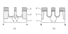
【解決手段】第1の溝内の素子分離膜と活性領域を有する半導体基板を用意する工程と、この半導体基板上にマスク形成用膜を形成する工程と、活性領域を横切る開口を有する第1のマスクを形成する工程と、第1のマスクを用いて異方性エッチングを行って、前記マスク形成用膜からなる第2のマスクと、活性領域内に、対向する素子分離膜露出面を有し且つ第1の溝より浅い第2の溝を形成する工程と、第2の溝内の半導体基板表面と素子分離膜露出面との境界を含む領域に酸素イオンが照射されるように、第2のマスクを用いて酸素イオンを斜めに注入する工程と、第2の溝内の酸素イオンが注入された領域を酸化して酸化領域を形成する工程と、この酸化領域を除去する工程を有する半導体装置の製造方法。
【選択図】図5
Description
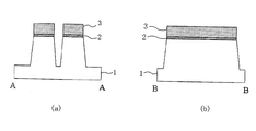
第1の溝と、第1の溝内に埋め込まれた素子分離膜と、この素子分離膜に囲まれた活性領域を有する半導体基板を用意する工程と、
前記半導体基板上にマスク形成用膜を形成する工程と、
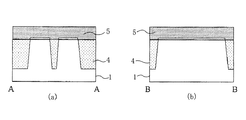
前記マスク形成用膜上に、前記活性領域を横切る開口を有する第1のマスクを形成する工程と、
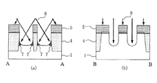
第1のマスクを用いて異方性エッチングを行って、前記開口に対応する開口を有する前記マスク形成用膜からなる第2のマスクと、前記活性領域内に、対向する素子分離膜露出面を有し且つ第1の溝より浅い第2の溝を形成する工程と、
第2の溝内の半導体基板表面と素子分離膜露出面との境界を含む領域に酸素イオンが照射されるように、第2の溝内に、第2のマスクを用いて、酸素イオンを斜めに注入する工程と、
第2の溝内の酸素イオンが注入された領域を酸化して酸化領域を形成する工程と、
前記酸化領域を除去する工程を有する半導体装置の製造方法が提供される。
第2の溝内を含む半導体基板表面の酸化を行って、第2の溝内の酸素イオンが注入された領域を酸化して酸化領域を形成するとともに、この酸化領域を含む酸化膜を形成する工程と、
前記酸化膜を除去するとともに、前記酸化領域を除去する工程を有する上記の半導体装置の製造方法が提供される。
第2の絶縁膜を除去する工程と、
第2の溝内を含む半導体基板上にゲート絶縁膜を形成する工程と、
前記ゲート絶縁膜が形成された第2の溝内を埋め込むように導電膜を形成し、この導電膜をパターニングしてゲート電極を形成する工程と、
前記ゲート電極の両側の当該活性領域に不純物を導入してソース/ドレイン領域を形成する工程をさらに有する上記の半導体装置の製造方法が提供される。
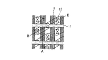
2 酸化シリコン膜
3 窒化シリコン膜
4 素子分離膜
5 窒化シリコン膜
6 溝
7 取り残り部(バリ)
8 酸素イオン注入
9 犠牲酸化膜(酸化シリコン膜)
10 ゲート絶縁膜(酸化シリコン膜)
11 ゲート電極
12 コンタクトプラグ
13 ビット線
Claims (4)
- 第1の溝と、第1の溝内に埋め込まれた素子分離膜と、この素子分離膜に囲まれた活性領域を有する半導体基板を用意する工程と、
前記半導体基板上にマスク形成用膜を形成する工程と、
前記マスク形成用膜上に、前記活性領域を横切る開口を有する第1のマスクを形成する工程と、
第1のマスクを用いて異方性エッチングを行って、前記開口に対応する開口を有する前記マスク形成用膜からなる第2のマスクと、前記活性領域内に、対向する素子分離膜露出面を有し且つ第1の溝より浅い第2の溝を形成する工程と、
第2の溝内の半導体基板表面と素子分離膜露出面との境界を含む領域に酸素イオンが照射されるように、第2の溝内に、第2のマスクを用いて、酸素イオンを斜めに注入する工程と、
第2の溝内の酸素イオンが注入された領域を酸化して酸化領域を形成する工程と、
前記酸化領域を除去する工程を有する半導体装置の製造方法。 - 第2の溝内を含む半導体基板表面の酸化を行って、第2の溝内の酸素イオンが注入された領域を酸化して酸化領域を形成するとともに、この酸化領域を含む酸化膜を形成する工程と、
前記酸化膜を除去するとともに、前記酸化領域を除去する工程を有する請求項1に記載の半導体装置の製造方法。 - 第2のマスクを除去する工程と、
第2の溝内を含む半導体基板上にゲート絶縁膜を形成する工程と、
前記ゲート絶縁膜が形成された第2の溝内を埋め込むように導電膜を形成し、この導電膜をパターニングしてゲート電極を形成する工程と、
前記ゲート電極の両側の当該活性領域に不純物を導入してソース/ドレイン領域を形成する工程をさらに有する請求項1又は2に記載の半導体装置の製造方法。 - 前記素子分離膜は酸化シリコン膜、前記マスク形成用膜は窒化シリコン膜である請求項1から3のいずれかに記載の半導体装置の製造方法。
Priority Applications (2)
| Application Number | Priority Date | Filing Date | Title |
|---|---|---|---|
| JP2007162424A JP2009004480A (ja) | 2007-06-20 | 2007-06-20 | 半導体装置の製造方法 |
| US12/142,320 US20080318383A1 (en) | 2007-06-20 | 2008-06-19 | Method of manufacturing semiconductor device |
Applications Claiming Priority (1)
| Application Number | Priority Date | Filing Date | Title |
|---|---|---|---|
| JP2007162424A JP2009004480A (ja) | 2007-06-20 | 2007-06-20 | 半導体装置の製造方法 |
Publications (2)
| Publication Number | Publication Date |
|---|---|
| JP2009004480A true JP2009004480A (ja) | 2009-01-08 |
| JP2009004480A5 JP2009004480A5 (ja) | 2010-07-08 |
Family
ID=40136921
Family Applications (1)
| Application Number | Title | Priority Date | Filing Date |
|---|---|---|---|
| JP2007162424A Pending JP2009004480A (ja) | 2007-06-20 | 2007-06-20 | 半導体装置の製造方法 |
Country Status (2)
| Country | Link |
|---|---|
| US (1) | US20080318383A1 (ja) |
| JP (1) | JP2009004480A (ja) |
Cited By (1)
| Publication number | Priority date | Publication date | Assignee | Title |
|---|---|---|---|---|
| KR101802371B1 (ko) * | 2011-05-12 | 2017-11-29 | 에스케이하이닉스 주식회사 | 반도체 셀 및 그 형성 방법 |
Families Citing this family (1)
| Publication number | Priority date | Publication date | Assignee | Title |
|---|---|---|---|---|
| CN113054014A (zh) * | 2019-12-26 | 2021-06-29 | 株洲中车时代半导体有限公司 | SiC沟槽氧化层和SiC MOSFET沟槽栅的制备方法及SiC MOSFET器件 |
Citations (2)
| Publication number | Priority date | Publication date | Assignee | Title |
|---|---|---|---|---|
| JP2000243954A (ja) * | 1999-02-22 | 2000-09-08 | Oki Electric Ind Co Ltd | 半導体装置の製造方法 |
| JP2005183976A (ja) * | 2003-12-19 | 2005-07-07 | Samsung Electronics Co Ltd | シリコン基板とのエッチング選択比が大きいマスク層を用いたリセスチャンネルアレイトランジスタの製造方法 |
Family Cites Families (2)
| Publication number | Priority date | Publication date | Assignee | Title |
|---|---|---|---|---|
| KR100468771B1 (ko) * | 2002-10-10 | 2005-01-29 | 삼성전자주식회사 | 모스 트랜지스터의 제조방법 |
| KR100604816B1 (ko) * | 2003-05-19 | 2006-07-28 | 삼성전자주식회사 | 집적 회로 소자 리세스 트랜지스터의 제조 방법 및 이에의해 제조된 집적회로 소자 리세스 트랜지스터 |
-
2007
- 2007-06-20 JP JP2007162424A patent/JP2009004480A/ja active Pending
-
2008
- 2008-06-19 US US12/142,320 patent/US20080318383A1/en not_active Abandoned
Patent Citations (2)
| Publication number | Priority date | Publication date | Assignee | Title |
|---|---|---|---|---|
| JP2000243954A (ja) * | 1999-02-22 | 2000-09-08 | Oki Electric Ind Co Ltd | 半導体装置の製造方法 |
| JP2005183976A (ja) * | 2003-12-19 | 2005-07-07 | Samsung Electronics Co Ltd | シリコン基板とのエッチング選択比が大きいマスク層を用いたリセスチャンネルアレイトランジスタの製造方法 |
Cited By (1)
| Publication number | Priority date | Publication date | Assignee | Title |
|---|---|---|---|---|
| KR101802371B1 (ko) * | 2011-05-12 | 2017-11-29 | 에스케이하이닉스 주식회사 | 반도체 셀 및 그 형성 방법 |
Also Published As
| Publication number | Publication date |
|---|---|
| US20080318383A1 (en) | 2008-12-25 |
Similar Documents
| Publication | Publication Date | Title |
|---|---|---|
| US7858490B2 (en) | Semiconductor device having dual-STI and manufacturing method thereof | |
| US7659179B2 (en) | Method of forming transistor using step STI profile in memory device | |
| JP2000200878A (ja) | 半導体集積回路装置およびその製造方法 | |
| JP2010027904A (ja) | 半導体装置の製造方法 | |
| US8198674B2 (en) | Semiconductor device and manufacturing method thereof | |
| US20120286357A1 (en) | Sense-amp transistor of semiconductor device and method for manufacturing the same | |
| JP2007194333A (ja) | 半導体装置の製造方法 | |
| JP2008053274A (ja) | 半導体装置及びその製造方法 | |
| JP2009004480A (ja) | 半導体装置の製造方法 | |
| US20090011564A1 (en) | Method of forming a gate oxide layer | |
| JP2005116952A (ja) | トレンチキャパシタ及びその製造方法 | |
| JP4191203B2 (ja) | 半導体装置及びその製造方法 | |
| JP2006310484A (ja) | 半導体装置の製造方法 | |
| KR101044385B1 (ko) | 반도체 소자의 제조방법 | |
| KR101098590B1 (ko) | 리세스 게이트를 갖는 반도체 소자의 제조방법 | |
| US7696075B2 (en) | Method of fabricating semiconductor device having a recess channel structure therein | |
| JP2011103436A (ja) | 半導体素子及びその製造方法 | |
| JP4989076B2 (ja) | 半導体装置の製造方法 | |
| JP2009004492A (ja) | 半導体装置の製造方法 | |
| KR20030094441A (ko) | 반도체 소자의 소자 분리막 형성 방법 | |
| KR20080089016A (ko) | 반도체 소자의 제조 방법 | |
| JP2008218808A (ja) | 半導体装置およびその製造方法 | |
| JP2005093816A (ja) | 半導体装置の製造方法および半導体装置 | |
| KR20140028907A (ko) | 반도체 소자의 제조방법 | |
| JPH06244415A (ja) | 半導体装置およびその製造方法 |
Legal Events
| Date | Code | Title | Description |
|---|---|---|---|
| A521 | Request for written amendment filed |
Free format text: JAPANESE INTERMEDIATE CODE: A523 Effective date: 20100520 |
|
| A621 | Written request for application examination |
Free format text: JAPANESE INTERMEDIATE CODE: A621 Effective date: 20100520 |
|
| A711 | Notification of change in applicant |
Free format text: JAPANESE INTERMEDIATE CODE: A711 Effective date: 20130730 |
|
| A977 | Report on retrieval |
Free format text: JAPANESE INTERMEDIATE CODE: A971007 Effective date: 20131209 |
|
| A131 | Notification of reasons for refusal |
Free format text: JAPANESE INTERMEDIATE CODE: A131 Effective date: 20131217 |
|
| A601 | Written request for extension of time |
Free format text: JAPANESE INTERMEDIATE CODE: A601 Effective date: 20140317 |
|
| A602 | Written permission of extension of time |
Free format text: JAPANESE INTERMEDIATE CODE: A602 Effective date: 20140320 |
|
| A601 | Written request for extension of time |
Free format text: JAPANESE INTERMEDIATE CODE: A601 Effective date: 20140325 |
|
| A602 | Written permission of extension of time |
Free format text: JAPANESE INTERMEDIATE CODE: A602 Effective date: 20140328 |
|
| RD04 | Notification of resignation of power of attorney |
Free format text: JAPANESE INTERMEDIATE CODE: A7424 Effective date: 20140410 |
|
| A02 | Decision of refusal |
Free format text: JAPANESE INTERMEDIATE CODE: A02 Effective date: 20141111 |