JP2008166310A - 半田印刷マスク、プリント配線基板及び回路基板の製造方法 - Google Patents
半田印刷マスク、プリント配線基板及び回路基板の製造方法 Download PDFInfo
- Publication number
- JP2008166310A JP2008166310A JP2006350652A JP2006350652A JP2008166310A JP 2008166310 A JP2008166310 A JP 2008166310A JP 2006350652 A JP2006350652 A JP 2006350652A JP 2006350652 A JP2006350652 A JP 2006350652A JP 2008166310 A JP2008166310 A JP 2008166310A
- Authority
- JP
- Japan
- Prior art keywords
- land
- component
- solder
- mounting
- printed wiring
- Prior art date
- Legal status (The legal status is an assumption and is not a legal conclusion. Google has not performed a legal analysis and makes no representation as to the accuracy of the status listed.)
- Pending
Links
Images

Landscapes
- Printing Plates And Materials Therefor (AREA)
- Electric Connection Of Electric Components To Printed Circuits (AREA)
Abstract
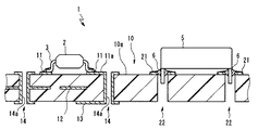
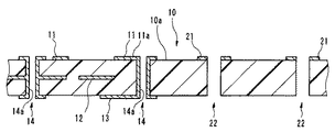
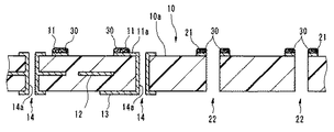
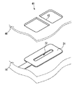
【解決手段】プリント配線基板の実装面上に、表面実装部品と挿入部品とが実装されてなる回路基板の製造方法において、表面実装部品が半田付けされる第1のランド上に半田ペーストを印刷するとともに、挿入部品が半田付けされる第2のランド上に半田ペーストが複数の領域に分割されて印刷されるように印刷する工程と、半田ペーストが印刷された第1のランド上に、表面実装部品を搭載する工程と、基板を加熱して表面実装部品を第1のランドに半田付けするとともに、第2のランド上に半田による被膜を形成する工程と、挿入部品を第2のランドに半田付けする工程とを実施するものとする。
【選択図】図8
Description
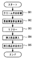
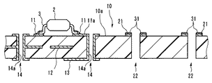
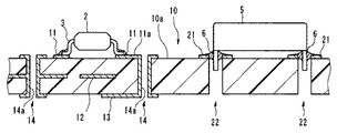
以上により、プリント配線基板10に、表面実装部品2及び挿入部品5が実装され、本実施形態の回路基板1の製造工程が終了するのである。
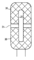
本実施形態の回路基板1の製造方法においては、ステップS01のクリーム半田印刷工程において、実装部品用ランド11上と挿入部品用ランド21上とに同時にクリーム半田30を印刷する場合に、挿入部品用ランド21上には、クリーム半田30が複数の領域に分割されて印刷される。
Claims (4)
- 表面実装部品及び挿入部品が実装されるプリント配線基板にクリーム半田を印刷するための半田印刷マスクであって、
前記挿入部品が半田付けされるランドに対応する開口部は、梁部が形成されることにより複数に分割されてなることを特徴とする半田印刷マスク。 - 複数の層の配線パターンを有し、実装面上に表面実装部品と挿入部品とが半田付けされるランドが形成されてなるプリント配線基板であって、
前記挿入部品が半田付けされる前記ランドを構成する導体部は、前記実装面上にのみに配設されることを特徴とするプリント配線基板。 - プリント配線基板の少なくとも一方の主面である実装面上に、表面実装部品と挿入部品とが実装されてなる回路基板の製造方法であって、
前記表面実装部品が半田付けされる第1のランド上に半田ペーストを印刷するとともに、前記挿入部品が半田付けされる第2のランド上に前記半田ペーストが複数の領域に分割されて印刷されるように印刷する工程と、
前記半田ペーストが印刷された第1のランド上に、前記表面実装部品を搭載する工程と、
前記基板を加熱して前記表面実装部品を前記第1のランドに半田付けするとともに、前記第2のランド上に半田による被膜を形成する工程と、
前記挿入部品を前記第2のランドに半田付けする工程とを具備することを特徴とする回路基板の製造方法。 - 前記プリント配線基板は、複数の層の配線パターンを有してなり、
前記第2のランドを構成する導体部は、前記実装面上にのみに配設されることを特徴とする請求項3に記載の回路基板の製造方法。
Priority Applications (1)
| Application Number | Priority Date | Filing Date | Title |
|---|---|---|---|
| JP2006350652A JP2008166310A (ja) | 2006-12-26 | 2006-12-26 | 半田印刷マスク、プリント配線基板及び回路基板の製造方法 |
Applications Claiming Priority (1)
| Application Number | Priority Date | Filing Date | Title |
|---|---|---|---|
| JP2006350652A JP2008166310A (ja) | 2006-12-26 | 2006-12-26 | 半田印刷マスク、プリント配線基板及び回路基板の製造方法 |
Publications (1)
| Publication Number | Publication Date |
|---|---|
| JP2008166310A true JP2008166310A (ja) | 2008-07-17 |
Family
ID=39695447
Family Applications (1)
| Application Number | Title | Priority Date | Filing Date |
|---|---|---|---|
| JP2006350652A Pending JP2008166310A (ja) | 2006-12-26 | 2006-12-26 | 半田印刷マスク、プリント配線基板及び回路基板の製造方法 |
Country Status (1)
| Country | Link |
|---|---|
| JP (1) | JP2008166310A (ja) |
Cited By (4)
| Publication number | Priority date | Publication date | Assignee | Title |
|---|---|---|---|---|
| EP2139056A1 (en) | 2008-06-25 | 2009-12-30 | Sony Corporation | Female connector structure, male connector structure, battery, adaptor and electric device |
| JP2011082498A (ja) * | 2009-10-07 | 2011-04-21 | Samsung Electro-Mechanics Co Ltd | ハンダを印刷するためのマスク及びこれを用いた印刷回路基板の製造方法 |
| CN113455112A (zh) * | 2019-02-25 | 2021-09-28 | 三菱电机株式会社 | 电路基板、半导体装置、电力转换装置及移动体 |
| CN115103528A (zh) * | 2022-06-20 | 2022-09-23 | 珠海景旺柔性电路有限公司 | 柔性电路板连接器焊接方法及柔性电路板 |
Citations (2)
| Publication number | Priority date | Publication date | Assignee | Title |
|---|---|---|---|---|
| JPH09162536A (ja) * | 1995-12-06 | 1997-06-20 | Sony Corp | 印刷回路基板への部品実装方法および印刷回路基板に実装する部品ならびに印刷回路基板 |
| JP2002185116A (ja) * | 2000-12-18 | 2002-06-28 | Rb Controls Co | メタルマスク及びクリーム半田印刷方法 |
-
2006
- 2006-12-26 JP JP2006350652A patent/JP2008166310A/ja active Pending
Patent Citations (2)
| Publication number | Priority date | Publication date | Assignee | Title |
|---|---|---|---|---|
| JPH09162536A (ja) * | 1995-12-06 | 1997-06-20 | Sony Corp | 印刷回路基板への部品実装方法および印刷回路基板に実装する部品ならびに印刷回路基板 |
| JP2002185116A (ja) * | 2000-12-18 | 2002-06-28 | Rb Controls Co | メタルマスク及びクリーム半田印刷方法 |
Cited By (4)
| Publication number | Priority date | Publication date | Assignee | Title |
|---|---|---|---|---|
| EP2139056A1 (en) | 2008-06-25 | 2009-12-30 | Sony Corporation | Female connector structure, male connector structure, battery, adaptor and electric device |
| JP2011082498A (ja) * | 2009-10-07 | 2011-04-21 | Samsung Electro-Mechanics Co Ltd | ハンダを印刷するためのマスク及びこれを用いた印刷回路基板の製造方法 |
| CN113455112A (zh) * | 2019-02-25 | 2021-09-28 | 三菱电机株式会社 | 电路基板、半导体装置、电力转换装置及移动体 |
| CN115103528A (zh) * | 2022-06-20 | 2022-09-23 | 珠海景旺柔性电路有限公司 | 柔性电路板连接器焊接方法及柔性电路板 |
Similar Documents
| Publication | Publication Date | Title |
|---|---|---|
| JP7522973B2 (ja) | チップ部品の実装構造 | |
| JP2008166310A (ja) | 半田印刷マスク、プリント配線基板及び回路基板の製造方法 | |
| JP5938953B2 (ja) | プリント配線基板の反り低減構造および回路基板の製造方法 | |
| JPH07288375A (ja) | 回路基板 | |
| KR20060045757A (ko) | 프린트 배선 기판, 부품 실장 방법 및 탑재 위치 확인 방법 | |
| US6344974B1 (en) | Printed circuit board and method of producing same | |
| JP2010103295A (ja) | 端面スルーホール配線基板の製造方法 | |
| JP2007027538A (ja) | 回路基板 | |
| US20070089903A1 (en) | Printed circuit board | |
| JP2001102713A (ja) | ピン立て型プリント回路基板 | |
| KR20090102227A (ko) | 인쇄회로기판 및 그 제조방법 | |
| JP2008205101A (ja) | 電子部品実装基板の製造方法及び電子部品実装基板 | |
| US20060038264A1 (en) | Printed circuit board | |
| JP2009060006A (ja) | 半田付けパレット | |
| JPH06296076A (ja) | Smdモジュールの側面電極形成方法 | |
| JP2002334953A (ja) | 配線基板の加工方法 | |
| JP2001102706A (ja) | ピン立て型プリント回路基板 | |
| JP2008066344A (ja) | 多層基板と金属接合材料の印刷方法 | |
| JP7427378B2 (ja) | プリント基板 | |
| JPS5853890A (ja) | 電子部品のはんだ付け方法 | |
| JP2020064998A5 (ja) | ||
| KR200176365Y1 (ko) | 인쇄회로기판 | |
| JP2017220574A (ja) | 電子部品実装基板の製造方法、基板およびメタルマスク | |
| EP2086298B1 (en) | Solder void reduction on circuit boards | |
| JP2007242906A (ja) | プリント配線板 |
Legal Events
| Date | Code | Title | Description |
|---|---|---|---|
| A621 | Written request for application examination |
Effective date: 20091008 Free format text: JAPANESE INTERMEDIATE CODE: A621 |
|
| A977 | Report on retrieval |
Free format text: JAPANESE INTERMEDIATE CODE: A971007 Effective date: 20110301 |
|
| A131 | Notification of reasons for refusal |
Effective date: 20110308 Free format text: JAPANESE INTERMEDIATE CODE: A131 |
|
| A521 | Written amendment |
Free format text: JAPANESE INTERMEDIATE CODE: A523 Effective date: 20110420 |
|
| A131 | Notification of reasons for refusal |
Free format text: JAPANESE INTERMEDIATE CODE: A131 Effective date: 20110531 |
|
| A02 | Decision of refusal |
Effective date: 20111011 Free format text: JAPANESE INTERMEDIATE CODE: A02 |