JP2007273275A - 有機el発光装置 - Google Patents
有機el発光装置 Download PDFInfo
- Publication number
- JP2007273275A JP2007273275A JP2006098001A JP2006098001A JP2007273275A JP 2007273275 A JP2007273275 A JP 2007273275A JP 2006098001 A JP2006098001 A JP 2006098001A JP 2006098001 A JP2006098001 A JP 2006098001A JP 2007273275 A JP2007273275 A JP 2007273275A
- Authority
- JP
- Japan
- Prior art keywords
- light
- prism
- organic
- emitting device
- degrees
- Prior art date
- Legal status (The legal status is an assumption and is not a legal conclusion. Google has not performed a legal analysis and makes no representation as to the accuracy of the status listed.)
- Pending
Links
- 238000000605 extraction Methods 0.000 claims abstract description 35
- 239000000758 substrate Substances 0.000 claims description 11
- 150000002894 organic compounds Chemical class 0.000 claims description 4
- 230000010287 polarization Effects 0.000 abstract description 5
- 239000010410 layer Substances 0.000 description 18
- 230000000694 effects Effects 0.000 description 13
- 238000000034 method Methods 0.000 description 9
- 239000000463 material Substances 0.000 description 8
- 239000011347 resin Substances 0.000 description 6
- 229920005989 resin Polymers 0.000 description 6
- 238000004088 simulation Methods 0.000 description 6
- 238000011156 evaluation Methods 0.000 description 5
- 230000005855 radiation Effects 0.000 description 5
- 230000005525 hole transport Effects 0.000 description 4
- TVIVIEFSHFOWTE-UHFFFAOYSA-K tri(quinolin-8-yloxy)alumane Chemical compound [Al+3].C1=CN=C2C([O-])=CC=CC2=C1.C1=CN=C2C([O-])=CC=CC2=C1.C1=CN=C2C([O-])=CC=CC2=C1 TVIVIEFSHFOWTE-UHFFFAOYSA-K 0.000 description 4
- 230000008859 change Effects 0.000 description 3
- 238000001723 curing Methods 0.000 description 3
- 239000006185 dispersion Substances 0.000 description 3
- 239000011521 glass Substances 0.000 description 3
- 230000001681 protective effect Effects 0.000 description 3
- 239000004925 Acrylic resin Substances 0.000 description 2
- 229920000178 Acrylic resin Polymers 0.000 description 2
- NIXOWILDQLNWCW-UHFFFAOYSA-N acrylic acid group Chemical group C(C=C)(=O)O NIXOWILDQLNWCW-UHFFFAOYSA-N 0.000 description 2
- 238000013459 approach Methods 0.000 description 2
- 230000008901 benefit Effects 0.000 description 2
- 230000015572 biosynthetic process Effects 0.000 description 2
- 230000007423 decrease Effects 0.000 description 2
- 238000000151 deposition Methods 0.000 description 2
- 238000010586 diagram Methods 0.000 description 2
- 238000005516 engineering process Methods 0.000 description 2
- 230000004907 flux Effects 0.000 description 2
- 238000002347 injection Methods 0.000 description 2
- 239000007924 injection Substances 0.000 description 2
- 239000004973 liquid crystal related substance Substances 0.000 description 2
- 238000004519 manufacturing process Methods 0.000 description 2
- 230000003287 optical effect Effects 0.000 description 2
- 229920003229 poly(methyl methacrylate) Polymers 0.000 description 2
- 239000004417 polycarbonate Substances 0.000 description 2
- 229920000515 polycarbonate Polymers 0.000 description 2
- 239000004926 polymethyl methacrylate Substances 0.000 description 2
- 230000002265 prevention Effects 0.000 description 2
- 239000011241 protective layer Substances 0.000 description 2
- 238000004544 sputter deposition Methods 0.000 description 2
- ZCYVEMRRCGMTRW-UHFFFAOYSA-N 7553-56-2 Chemical compound [I] ZCYVEMRRCGMTRW-UHFFFAOYSA-N 0.000 description 1
- ZOXJGFHDIHLPTG-UHFFFAOYSA-N Boron Chemical compound [B] ZOXJGFHDIHLPTG-UHFFFAOYSA-N 0.000 description 1
- 229920002284 Cellulose triacetate Polymers 0.000 description 1
- RYGMFSIKBFXOCR-UHFFFAOYSA-N Copper Chemical compound [Cu] RYGMFSIKBFXOCR-UHFFFAOYSA-N 0.000 description 1
- 208000033962 Fontaine progeroid syndrome Diseases 0.000 description 1
- 238000000342 Monte Carlo simulation Methods 0.000 description 1
- 239000004372 Polyvinyl alcohol Substances 0.000 description 1
- XUIMIQQOPSSXEZ-UHFFFAOYSA-N Silicon Chemical compound [Si] XUIMIQQOPSSXEZ-UHFFFAOYSA-N 0.000 description 1
- UCKMPCXJQFINFW-UHFFFAOYSA-N Sulphide Chemical compound [S-2] UCKMPCXJQFINFW-UHFFFAOYSA-N 0.000 description 1
- NNLVGZFZQQXQNW-ADJNRHBOSA-N [(2r,3r,4s,5r,6s)-4,5-diacetyloxy-3-[(2s,3r,4s,5r,6r)-3,4,5-triacetyloxy-6-(acetyloxymethyl)oxan-2-yl]oxy-6-[(2r,3r,4s,5r,6s)-4,5,6-triacetyloxy-2-(acetyloxymethyl)oxan-3-yl]oxyoxan-2-yl]methyl acetate Chemical compound O([C@@H]1O[C@@H]([C@H]([C@H](OC(C)=O)[C@H]1OC(C)=O)O[C@H]1[C@@H]([C@@H](OC(C)=O)[C@H](OC(C)=O)[C@@H](COC(C)=O)O1)OC(C)=O)COC(=O)C)[C@@H]1[C@@H](COC(C)=O)O[C@@H](OC(C)=O)[C@H](OC(C)=O)[C@H]1OC(C)=O NNLVGZFZQQXQNW-ADJNRHBOSA-N 0.000 description 1
- QVGXLLKOCUKJST-UHFFFAOYSA-N atomic oxygen Chemical compound [O] QVGXLLKOCUKJST-UHFFFAOYSA-N 0.000 description 1
- 230000000903 blocking effect Effects 0.000 description 1
- 229910052796 boron Inorganic materials 0.000 description 1
- FJDQFPXHSGXQBY-UHFFFAOYSA-L caesium carbonate Chemical compound [Cs+].[Cs+].[O-]C([O-])=O FJDQFPXHSGXQBY-UHFFFAOYSA-L 0.000 description 1
- 229910000024 caesium carbonate Inorganic materials 0.000 description 1
- 238000004364 calculation method Methods 0.000 description 1
- 239000011248 coating agent Substances 0.000 description 1
- 238000000576 coating method Methods 0.000 description 1
- 230000000052 comparative effect Effects 0.000 description 1
- 238000000748 compression moulding Methods 0.000 description 1
- 229910052802 copper Inorganic materials 0.000 description 1
- 239000010949 copper Substances 0.000 description 1
- 238000005520 cutting process Methods 0.000 description 1
- 229910003460 diamond Inorganic materials 0.000 description 1
- 239000010432 diamond Substances 0.000 description 1
- 239000007772 electrode material Substances 0.000 description 1
- 238000005323 electroforming Methods 0.000 description 1
- 239000000284 extract Substances 0.000 description 1
- 229910052732 germanium Inorganic materials 0.000 description 1
- GNPVGFCGXDBREM-UHFFFAOYSA-N germanium atom Chemical compound [Ge] GNPVGFCGXDBREM-UHFFFAOYSA-N 0.000 description 1
- 230000006872 improvement Effects 0.000 description 1
- 229910052740 iodine Inorganic materials 0.000 description 1
- 239000011630 iodine Substances 0.000 description 1
- 230000001678 irradiating effect Effects 0.000 description 1
- 238000010030 laminating Methods 0.000 description 1
- 238000005259 measurement Methods 0.000 description 1
- 229910052751 metal Inorganic materials 0.000 description 1
- 239000002184 metal Substances 0.000 description 1
- IBHBKWKFFTZAHE-UHFFFAOYSA-N n-[4-[4-(n-naphthalen-1-ylanilino)phenyl]phenyl]-n-phenylnaphthalen-1-amine Chemical compound C1=CC=CC=C1N(C=1C2=CC=CC=C2C=CC=1)C1=CC=C(C=2C=CC(=CC=2)N(C=2C=CC=CC=2)C=2C3=CC=CC=C3C=CC=2)C=C1 IBHBKWKFFTZAHE-UHFFFAOYSA-N 0.000 description 1
- 150000004767 nitrides Chemical class 0.000 description 1
- 229910052760 oxygen Inorganic materials 0.000 description 1
- 239000001301 oxygen Substances 0.000 description 1
- 238000000016 photochemical curing Methods 0.000 description 1
- 238000000206 photolithography Methods 0.000 description 1
- 238000007747 plating Methods 0.000 description 1
- 229920006289 polycarbonate film Polymers 0.000 description 1
- 229920002451 polyvinyl alcohol Polymers 0.000 description 1
- 238000007639 printing Methods 0.000 description 1
- 230000008569 process Effects 0.000 description 1
- 238000002310 reflectometry Methods 0.000 description 1
- 238000011160 research Methods 0.000 description 1
- 238000004904 shortening Methods 0.000 description 1
- 229910052710 silicon Inorganic materials 0.000 description 1
- 239000010703 silicon Substances 0.000 description 1
- 229910052709 silver Inorganic materials 0.000 description 1
- ILJSQTXMGCGYMG-UHFFFAOYSA-N triacetic acid Chemical compound CC(=O)CC(=O)CC(O)=O ILJSQTXMGCGYMG-UHFFFAOYSA-N 0.000 description 1
- 238000001771 vacuum deposition Methods 0.000 description 1
- 229910052724 xenon Inorganic materials 0.000 description 1
- FHNFHKCVQCLJFQ-UHFFFAOYSA-N xenon atom Chemical compound [Xe] FHNFHKCVQCLJFQ-UHFFFAOYSA-N 0.000 description 1
Images


Classifications
-
- G—PHYSICS
- G02—OPTICS
- G02F—OPTICAL DEVICES OR ARRANGEMENTS FOR THE CONTROL OF LIGHT BY MODIFICATION OF THE OPTICAL PROPERTIES OF THE MEDIA OF THE ELEMENTS INVOLVED THEREIN; NON-LINEAR OPTICS; FREQUENCY-CHANGING OF LIGHT; OPTICAL LOGIC ELEMENTS; OPTICAL ANALOGUE/DIGITAL CONVERTERS
- G02F1/00—Devices or arrangements for the control of the intensity, colour, phase, polarisation or direction of light arriving from an independent light source, e.g. switching, gating or modulating; Non-linear optics
- G02F1/01—Devices or arrangements for the control of the intensity, colour, phase, polarisation or direction of light arriving from an independent light source, e.g. switching, gating or modulating; Non-linear optics for the control of the intensity, phase, polarisation or colour
- G02F1/13—Devices or arrangements for the control of the intensity, colour, phase, polarisation or direction of light arriving from an independent light source, e.g. switching, gating or modulating; Non-linear optics for the control of the intensity, phase, polarisation or colour based on liquid crystals, e.g. single liquid crystal display cells
- G02F1/133—Constructional arrangements; Operation of liquid crystal cells; Circuit arrangements
- G02F1/1333—Constructional arrangements; Manufacturing methods
- G02F1/1335—Structural association of cells with optical devices, e.g. polarisers or reflectors
- G02F1/1336—Illuminating devices
- G02F1/133602—Direct backlight
- G02F1/133606—Direct backlight including a specially adapted diffusing, scattering or light controlling members
-
- F—MECHANICAL ENGINEERING; LIGHTING; HEATING; WEAPONS; BLASTING
- F21—LIGHTING
- F21V—FUNCTIONAL FEATURES OR DETAILS OF LIGHTING DEVICES OR SYSTEMS THEREOF; STRUCTURAL COMBINATIONS OF LIGHTING DEVICES WITH OTHER ARTICLES, NOT OTHERWISE PROVIDED FOR
- F21V5/00—Refractors for light sources
- F21V5/02—Refractors for light sources of prismatic shape
-
- G—PHYSICS
- G02—OPTICS
- G02F—OPTICAL DEVICES OR ARRANGEMENTS FOR THE CONTROL OF LIGHT BY MODIFICATION OF THE OPTICAL PROPERTIES OF THE MEDIA OF THE ELEMENTS INVOLVED THEREIN; NON-LINEAR OPTICS; FREQUENCY-CHANGING OF LIGHT; OPTICAL LOGIC ELEMENTS; OPTICAL ANALOGUE/DIGITAL CONVERTERS
- G02F1/00—Devices or arrangements for the control of the intensity, colour, phase, polarisation or direction of light arriving from an independent light source, e.g. switching, gating or modulating; Non-linear optics
- G02F1/01—Devices or arrangements for the control of the intensity, colour, phase, polarisation or direction of light arriving from an independent light source, e.g. switching, gating or modulating; Non-linear optics for the control of the intensity, phase, polarisation or colour
- G02F1/13—Devices or arrangements for the control of the intensity, colour, phase, polarisation or direction of light arriving from an independent light source, e.g. switching, gating or modulating; Non-linear optics for the control of the intensity, phase, polarisation or colour based on liquid crystals, e.g. single liquid crystal display cells
- G02F1/133—Constructional arrangements; Operation of liquid crystal cells; Circuit arrangements
- G02F1/1333—Constructional arrangements; Manufacturing methods
- G02F1/1335—Structural association of cells with optical devices, e.g. polarisers or reflectors
- G02F1/1336—Illuminating devices
- G02F1/133602—Direct backlight
- G02F1/133603—Direct backlight with LEDs
-
- G—PHYSICS
- G02—OPTICS
- G02B—OPTICAL ELEMENTS, SYSTEMS OR APPARATUS
- G02B6/00—Light guides; Structural details of arrangements comprising light guides and other optical elements, e.g. couplings
- G02B6/0001—Light guides; Structural details of arrangements comprising light guides and other optical elements, e.g. couplings specially adapted for lighting devices or systems
- G02B6/0011—Light guides; Structural details of arrangements comprising light guides and other optical elements, e.g. couplings specially adapted for lighting devices or systems the light guides being planar or of plate-like form
- G02B6/0033—Means for improving the coupling-out of light from the light guide
- G02B6/005—Means for improving the coupling-out of light from the light guide provided by one optical element, or plurality thereof, placed on the light output side of the light guide
- G02B6/0053—Prismatic sheet or layer; Brightness enhancement element, sheet or layer
-
- G—PHYSICS
- G02—OPTICS
- G02F—OPTICAL DEVICES OR ARRANGEMENTS FOR THE CONTROL OF LIGHT BY MODIFICATION OF THE OPTICAL PROPERTIES OF THE MEDIA OF THE ELEMENTS INVOLVED THEREIN; NON-LINEAR OPTICS; FREQUENCY-CHANGING OF LIGHT; OPTICAL LOGIC ELEMENTS; OPTICAL ANALOGUE/DIGITAL CONVERTERS
- G02F1/00—Devices or arrangements for the control of the intensity, colour, phase, polarisation or direction of light arriving from an independent light source, e.g. switching, gating or modulating; Non-linear optics
- G02F1/01—Devices or arrangements for the control of the intensity, colour, phase, polarisation or direction of light arriving from an independent light source, e.g. switching, gating or modulating; Non-linear optics for the control of the intensity, phase, polarisation or colour
- G02F1/13—Devices or arrangements for the control of the intensity, colour, phase, polarisation or direction of light arriving from an independent light source, e.g. switching, gating or modulating; Non-linear optics for the control of the intensity, phase, polarisation or colour based on liquid crystals, e.g. single liquid crystal display cells
- G02F1/133—Constructional arrangements; Operation of liquid crystal cells; Circuit arrangements
- G02F1/1333—Constructional arrangements; Manufacturing methods
- G02F1/1335—Structural association of cells with optical devices, e.g. polarisers or reflectors
- G02F1/1336—Illuminating devices
- G02F1/133602—Direct backlight
- G02F1/133606—Direct backlight including a specially adapted diffusing, scattering or light controlling members
- G02F1/133607—Direct backlight including a specially adapted diffusing, scattering or light controlling members the light controlling member including light directing or refracting elements, e.g. prisms or lenses
Abstract
【解決手段】 有機EL素子10の光取り出し側にプリズム部材12、偏光部材13、位相差部材14を有し、プリズム部材12は複数の三角柱状の単位プリズムの長軸方向が互いに平行になるように配置されたプリズム部材である有機EL発光装置であって、偏光部材13はプリズム部材12よりも光取り出し側に配置され、プリズム部材12の頂角が90度以上140度以下である。
【選択図】 図1
Description
次に、本発明にかかる有機EL発光装置を構成する各部材について説明する。
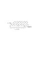
プリズム部材は有機EL素子の光取り出し面と接する面の反対側に凸部が複数設けられた光透過性を有する部材である。本発明における凸部の形状は、複数の三角柱状の単位プリズムの長軸方向が互いに平行になるように配置された形状である。
偏光部材はあらゆる方向に振動している光から一定方向にのみ振動する直線偏光を取り出すフィルターである。例えば一軸に延伸されたポリビニルアルコールフィルムにヨウ素などのニ色性色素を吸着配向させたものが使用される。
位相差部材は偏光部材によって偏光状態になった光に位相差を与える。本発明ではほぼλ/4の位相差を与え、直線偏光を円偏光に、円偏光を直線偏光に、それぞれ偏光状態を変える働きをもつ。材料としては、例えばポリカーボネートの一軸延伸配向フィルムなどが用いられる。
上記の偏光部材と位相差部材とを積層したものである。本発明においては、光取り出し側に偏光部材が配置される。円偏光部材を透過する光は、円偏光に変換される。また円偏光部材を透過する円偏光は位相差部材を透過する際に直線偏光に変換される。一度この円偏光部材を透過して、反射した円偏光は再度この円偏光部材を透過する際は偏光部材と直交する向きの偏光に変換されるため、偏光部材で吸収されて透過することはできない。
有機EL素子は、公知の素子構成、素子材料を適宜利用することができる。
次に、本発明の規定するプリズムの頂角について説明する。
プリズムの頂角を変化させた時の、EL発光の光取り出し効率を算出するために、市販の光線追跡シミュレーションソフトを用いた。光線追跡シミュレーション条件は以下のように設定した。
EL発光:発光層の中心平面より完全拡散発光
光線本数:2000本 モンテカルロシミュレーション
フレネル分岐数:50
(2)構成系のパラメーターの設定
アノード電極:完全反射
発光層:屈折率1.70 膜厚0.13μm
カソード電極:ITO 屈折率2.00 膜厚0.05μm
保護層: 屈折率1.53 膜厚50.0μm
プリズム:屈折率1.53 頂角20〜160度 ピッチ幅20μm
端面フレネル反射
次に外光反射防止について考察する。上述したようにプリズム部材が単に光を透過させるだけなら、円偏光部材との組み合わせにより外光反射を防止することができる。
(1)プリズム面への外光入射は、プリズム面に凹凸があることによって、プリズム面を基準とした時の入射角に依存して挙動が異なることを考慮する必要がある。
(2)また、入射角が大きくなると(後述するように、55度以上で)位相反転が起こることも考慮する必要がある。
(3)さらに、プリズム部材内で反射する回数に依存して位相反転の有無も異なってくることも考慮する必要がある。
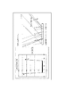
図4は評価×の例である。プリズムの頂角45度、外光15度入射条件では、複数回の多重反射がほとんどである。図5は評価○の例である。プリズムの頂角140度、外光15度入射条件では、1回反射のみでプリズム面への入射角度は5度と55度であった。
プリズム部材を付加した有機EL発光装置を以下の手順で作製した。
外光反射の影響を評価するために、ガラス基板にAlを蒸着した基板を用意した。それぞれ頂角の異なるプリズム部材をアクリル樹脂で接着し、この上に円偏光板を設けた。これらのサンプルを村上色彩技術研究所(株)製「3次元変角分光測色システム GCMS−11」で外光反射の影響を観察、評価した。具体的には標準白色光源(キセノンランプ)のほぼ平行光線を入射角度を変えながらサンプルに照射して、サンプル面を観察した。
この結果は、表3のシミュレーション予測である、複数回反射で外光反射が大きくなる、という結果とほぼ一致していた。○評価パネルのプリズム部材が見えにくいが、×評価パネルはいずれもプリズム部材が白っぽく見えてしまうことを確認した。特にプリズムの頂角60度以下では、特に顕著に白く見えた。

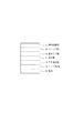
11 円偏光部材
12 プリズム部材
13 偏光部材
14 位相差部材
21 基板
22 アノード電極
23 正孔輸送層
24 発光層
25 電子輸送層
26 カソード電極
27 透明保護膜
Claims (7)
- 基材上の一対の電極間に配置される有機化合物層において発光する有機EL発光素子を有し、前記有機EL発光素子の光取り出し側にプリズム部材、偏光部材、位相差部材を有し、前記プリズム部材は複数の三角柱状の単位プリズムの長軸方向が互いに平行になるように配置されたプリズム部材である有機EL発光装置において、
前記偏光部材は前記プリズム部材よりも光取り出し側に配置され、
前記プリズム部材の頂角が90度以上140度以下であることを特徴とする有機EL発光装置。 - 前記光取り出し側から、前記偏光部材、前記位相差部材、前記プリズム部材、前記有機EL発光素子の順に配置されることを特徴とする請求項1に記載の有機EL発光装置。
- 前記光取り出し側から、前記偏光部材、前記プリズム部材、前記位相差部材、前記有機EL発光素子の順に配置されることを特徴とする請求項1に記載の有機EL発光装置。
- 前記有機EL発光装置が矩形のパネルであって、前記プリズム部材のピッチ方向と前記パネルの長尺方向とが一致することを特徴とする請求項1乃至請求項3のいずれか1項に記載の有機EL発光装置。
- 前記プリズム部材のプリズム面に反射防止処理がなされていることを特徴とする請求項1乃至請求項4のいずれか1項に記載の有機EL発光装置。
- 前記偏光部材の延伸方向と、隣接する前記プリズム部材の前記長軸方向が直交することを特徴とする請求項1乃至請求項5のいずれか1項に記載の有機EL発光装置。
- 前記有機化合物層において前記発光する光が、前記基材とは反対側から取り出されることを特徴とする請求項1乃至請求項6のいずれか1項に記載の有機EL発光装置。
Priority Applications (2)
| Application Number | Priority Date | Filing Date | Title |
|---|---|---|---|
| JP2006098001A JP2007273275A (ja) | 2006-03-31 | 2006-03-31 | 有機el発光装置 |
| US11/683,019 US7683533B2 (en) | 2006-03-31 | 2007-03-07 | Organic electroluminescent device provided with a polarizing plate, a prism member and a phase member in a stacked arrangement |
Applications Claiming Priority (1)
| Application Number | Priority Date | Filing Date | Title |
|---|---|---|---|
| JP2006098001A JP2007273275A (ja) | 2006-03-31 | 2006-03-31 | 有機el発光装置 |
Publications (2)
| Publication Number | Publication Date |
|---|---|
| JP2007273275A true JP2007273275A (ja) | 2007-10-18 |
| JP2007273275A5 JP2007273275A5 (ja) | 2007-11-29 |
Family
ID=38558621
Family Applications (1)
| Application Number | Title | Priority Date | Filing Date |
|---|---|---|---|
| JP2006098001A Pending JP2007273275A (ja) | 2006-03-31 | 2006-03-31 | 有機el発光装置 |
Country Status (2)
| Country | Link |
|---|---|
| US (1) | US7683533B2 (ja) |
| JP (1) | JP2007273275A (ja) |
Cited By (5)
| Publication number | Priority date | Publication date | Assignee | Title |
|---|---|---|---|---|
| WO2009084663A1 (ja) | 2007-12-28 | 2009-07-09 | Nippon Shokubai Co., Ltd. | 光学フィルムとそれを備える画像表示装置 |
| JP2012003074A (ja) * | 2010-06-17 | 2012-01-05 | Mitsubishi Rayon Co Ltd | 光学フィルム及びそれを用いた光学装置 |
| KR20140077707A (ko) * | 2012-12-14 | 2014-06-24 | 엘지디스플레이 주식회사 | 유기 발광 표시 장치 및 그의 제조 방법 |
| KR20170001634A (ko) * | 2015-06-26 | 2017-01-04 | 유니버셜 디스플레이 코포레이션 | 개선된 효율을 갖는 oled 디바이스 |
| KR20180036373A (ko) * | 2016-09-30 | 2018-04-09 | 엘지디스플레이 주식회사 | 표시장치 |
Families Citing this family (11)
| Publication number | Priority date | Publication date | Assignee | Title |
|---|---|---|---|---|
| JP4764230B2 (ja) * | 2006-03-31 | 2011-08-31 | キヤノン株式会社 | 表示装置 |
| JP2008108705A (ja) * | 2006-09-26 | 2008-05-08 | Canon Inc | 有機発光装置 |
| JP5224835B2 (ja) * | 2007-02-09 | 2013-07-03 | 国立大学法人東京工業大学 | 有機el素子およびその製造方法、ならびに有機el素子の評価方法 |
| JP2009272193A (ja) * | 2008-05-09 | 2009-11-19 | Funai Electric Co Ltd | バックライト装置及び液晶表示装置 |
| JP4947095B2 (ja) * | 2009-06-16 | 2012-06-06 | 住友化学株式会社 | 光取り出し構造体 |
| JP2011100715A (ja) * | 2009-10-09 | 2011-05-19 | Canon Inc | 発光装置、表示装置および撮像装置 |
| US9632326B2 (en) | 2010-10-28 | 2017-04-25 | Philips Lighting Holding B.V. | Collimator comprising a prismatic layer stack, and lighting unit comprising such collimator |
| BR112013021131A2 (pt) | 2011-02-22 | 2019-09-24 | Koninklijke Philips Electrnics N. V. | colimador compreendendo uma chaminé de camada prismática, e unidade de iluminação compreendendo o dito colimador |
| DE102012204062A1 (de) * | 2012-03-15 | 2013-09-19 | Ledon Oled Lighting Gmbh & Co. Kg | Lichtabgabeanordnung mit einer OLED oder QLED mit verbesserter Lichtausbeute |
| EP3033778A4 (en) | 2013-08-12 | 2017-03-29 | 3M Innovative Properties Company | Emissive article with light extraction film |
| CN104134758A (zh) * | 2014-07-14 | 2014-11-05 | 上海和辉光电有限公司 | 一种oled显示屏的封装结构 |
Citations (9)
| Publication number | Priority date | Publication date | Assignee | Title |
|---|---|---|---|---|
| JPH071428U (ja) * | 1993-06-04 | 1995-01-10 | 株式会社エンプラス | 面光源装置 |
| JPH118063A (ja) * | 1997-06-12 | 1999-01-12 | Minnesota Mining & Mfg Co <3M> | エレクトロルミネッセンス素子およびその製造方法 |
| JP2000321431A (ja) * | 1999-05-17 | 2000-11-24 | Nitto Denko Corp | 偏光素子、光学素子、偏光光源装置及び液晶表示装置 |
| JP2002006776A (ja) * | 2000-06-22 | 2002-01-11 | Nec Corp | 画像表示装置 |
| JP2004054035A (ja) * | 2002-07-22 | 2004-02-19 | Seiko Epson Corp | 液晶表示装置及び電子機器 |
| JP2005091825A (ja) * | 2003-09-18 | 2005-04-07 | Nippon Zeon Co Ltd | 偏光分離シート及び輝度向上フィルム |
| JP2006030289A (ja) * | 2004-07-12 | 2006-02-02 | Toshiba Matsushita Display Technology Co Ltd | El表示装置 |
| JP2006048011A (ja) * | 2004-06-29 | 2006-02-16 | Semiconductor Energy Lab Co Ltd | 表示装置及びその駆動方法並びに電子機器 |
| JP2006066074A (ja) * | 2004-08-24 | 2006-03-09 | Nippon Zeon Co Ltd | 直下型バックライト装置 |
Family Cites Families (11)
| Publication number | Priority date | Publication date | Assignee | Title |
|---|---|---|---|---|
| JPH0467016A (ja) | 1990-07-05 | 1992-03-03 | Sharp Corp | 液晶表示装置 |
| JPH06308485A (ja) | 1993-04-21 | 1994-11-04 | Hitachi Ltd | 表示装置 |
| US6804058B1 (en) * | 1993-12-21 | 2004-10-12 | 3M Innovative Properties Company | Electroluminescent light source and display incorporating same |
| JP3900617B2 (ja) | 1997-09-17 | 2007-04-04 | カシオ計算機株式会社 | 発光素子及び発光素子用の保護材料 |
| JP2002216947A (ja) | 2001-01-22 | 2002-08-02 | Polatechno Co Ltd | 表示装置 |
| JP2005055481A (ja) | 2003-06-09 | 2005-03-03 | Toyota Industries Corp | 光学素子、面状照明装置及び表示装置 |
| US7420322B2 (en) * | 2003-06-27 | 2008-09-02 | Casio Computer Co., Ltd. | Display device including a flat panel display panel |
| US20050242709A1 (en) * | 2004-04-30 | 2005-11-03 | Seiko Epson Corporation | Display element and method of manufacturing display element |
| US7440044B2 (en) * | 2004-11-29 | 2008-10-21 | Arisawa Manufacturing Co., Ltd. | Color display device and method |
| US8217572B2 (en) * | 2005-10-18 | 2012-07-10 | Semiconductor Energy Laboratory Co., Ltd. | Display device with prism layer |
| JP4764230B2 (ja) * | 2006-03-31 | 2011-08-31 | キヤノン株式会社 | 表示装置 |
-
2006
- 2006-03-31 JP JP2006098001A patent/JP2007273275A/ja active Pending
-
2007
- 2007-03-07 US US11/683,019 patent/US7683533B2/en not_active Expired - Fee Related
Patent Citations (9)
| Publication number | Priority date | Publication date | Assignee | Title |
|---|---|---|---|---|
| JPH071428U (ja) * | 1993-06-04 | 1995-01-10 | 株式会社エンプラス | 面光源装置 |
| JPH118063A (ja) * | 1997-06-12 | 1999-01-12 | Minnesota Mining & Mfg Co <3M> | エレクトロルミネッセンス素子およびその製造方法 |
| JP2000321431A (ja) * | 1999-05-17 | 2000-11-24 | Nitto Denko Corp | 偏光素子、光学素子、偏光光源装置及び液晶表示装置 |
| JP2002006776A (ja) * | 2000-06-22 | 2002-01-11 | Nec Corp | 画像表示装置 |
| JP2004054035A (ja) * | 2002-07-22 | 2004-02-19 | Seiko Epson Corp | 液晶表示装置及び電子機器 |
| JP2005091825A (ja) * | 2003-09-18 | 2005-04-07 | Nippon Zeon Co Ltd | 偏光分離シート及び輝度向上フィルム |
| JP2006048011A (ja) * | 2004-06-29 | 2006-02-16 | Semiconductor Energy Lab Co Ltd | 表示装置及びその駆動方法並びに電子機器 |
| JP2006030289A (ja) * | 2004-07-12 | 2006-02-02 | Toshiba Matsushita Display Technology Co Ltd | El表示装置 |
| JP2006066074A (ja) * | 2004-08-24 | 2006-03-09 | Nippon Zeon Co Ltd | 直下型バックライト装置 |
Cited By (11)
| Publication number | Priority date | Publication date | Assignee | Title |
|---|---|---|---|---|
| WO2009084663A1 (ja) | 2007-12-28 | 2009-07-09 | Nippon Shokubai Co., Ltd. | 光学フィルムとそれを備える画像表示装置 |
| JP2012003074A (ja) * | 2010-06-17 | 2012-01-05 | Mitsubishi Rayon Co Ltd | 光学フィルム及びそれを用いた光学装置 |
| KR20140077707A (ko) * | 2012-12-14 | 2014-06-24 | 엘지디스플레이 주식회사 | 유기 발광 표시 장치 및 그의 제조 방법 |
| KR102000050B1 (ko) * | 2012-12-14 | 2019-07-15 | 엘지디스플레이 주식회사 | 유기 발광 표시 장치 및 그의 제조 방법 |
| KR20170001634A (ko) * | 2015-06-26 | 2017-01-04 | 유니버셜 디스플레이 코포레이션 | 개선된 효율을 갖는 oled 디바이스 |
| JP2017017013A (ja) * | 2015-06-26 | 2017-01-19 | ユニバーサル ディスプレイ コーポレイション | 改善された効率を有するoledデバイス |
| US10686159B2 (en) | 2015-06-26 | 2020-06-16 | Universal Display Corporation | OLED devices having improved efficiency |
| US11121346B2 (en) | 2015-06-26 | 2021-09-14 | Universal Display Corporation | OLED devices having improved efficiency |
| KR102478347B1 (ko) * | 2015-06-26 | 2022-12-15 | 유니버셜 디스플레이 코포레이션 | 개선된 효율을 갖는 oled 디바이스 |
| KR20180036373A (ko) * | 2016-09-30 | 2018-04-09 | 엘지디스플레이 주식회사 | 표시장치 |
| KR102616406B1 (ko) * | 2016-09-30 | 2023-12-20 | 엘지디스플레이 주식회사 | 표시장치 |
Also Published As
| Publication number | Publication date |
|---|---|
| US20070230158A1 (en) | 2007-10-04 |
| US7683533B2 (en) | 2010-03-23 |
Similar Documents
| Publication | Publication Date | Title |
|---|---|---|
| JP2007273275A (ja) | 有機el発光装置 | |
| JP4764230B2 (ja) | 表示装置 | |
| JP2008108705A (ja) | 有機発光装置 | |
| JP5195719B2 (ja) | 液晶表示装置 | |
| TWI341948B (en) | Display device | |
| JP4122808B2 (ja) | 液晶表示装置および電子機器 | |
| JP2003332068A (ja) | エレクトロルミネッセンス素子 | |
| US20040001169A1 (en) | Polarizer, polarizing plate, liquid crystal display, and image display, and a method for producing the polarizer | |
| JP2014535127A (ja) | ディスプレイバックライトシステム | |
| KR20100056984A (ko) | 광학 시트, 조명 장치 및 액정 표시 장치 | |
| TW200307162A (en) | Liquid crystal display unit with wide viewing angle | |
| US20110037928A1 (en) | Wire grid polarizer for use on the front side oflcds | |
| KR101640719B1 (ko) | 액정표시장치용 모듈 및 이를 포함하는 액정표시장치 | |
| JP2010262813A (ja) | 照明装置及び液晶表示装置 | |
| CN104503129A (zh) | 一种光学模组和反射型显示装置 | |
| US20110073876A1 (en) | Light-emitting device and display | |
| KR102120808B1 (ko) | 색 변화 저감용 광학 필름 및 이를 채용한 유기 발광 표시 장치 | |
| CN103244875A (zh) | 一种具有纳米金属光栅的显示用背光结构 | |
| TW201608308A (zh) | 背光單元及液晶顯示裝置 | |
| US20020000772A1 (en) | Image display apparatus | |
| CN1400496A (zh) | 液晶显示装置及电子装置 | |
| KR20240017073A (ko) | 디스플레이 장치 및 전자 디바이스 | |
| JP2006244768A (ja) | エレクトロルミネッセンス素子 | |
| KR101813753B1 (ko) | 액정표시장치 | |
| CN1613028A (zh) | 背光灯及使用它的液晶显示装置 |
Legal Events
| Date | Code | Title | Description |
|---|---|---|---|
| A521 | Request for written amendment filed |
Free format text: JAPANESE INTERMEDIATE CODE: A523 Effective date: 20070830 |
|
| A621 | Written request for application examination |
Free format text: JAPANESE INTERMEDIATE CODE: A621 Effective date: 20070830 |
|
| RD04 | Notification of resignation of power of attorney |
Free format text: JAPANESE INTERMEDIATE CODE: A7424 Effective date: 20100201 |
|
| A131 | Notification of reasons for refusal |
Free format text: JAPANESE INTERMEDIATE CODE: A131 Effective date: 20100216 |
|
| A521 | Request for written amendment filed |
Free format text: JAPANESE INTERMEDIATE CODE: A523 Effective date: 20100414 |
|
| A02 | Decision of refusal |
Free format text: JAPANESE INTERMEDIATE CODE: A02 Effective date: 20100525 |
|
| RD01 | Notification of change of attorney |
Free format text: JAPANESE INTERMEDIATE CODE: A7421 Effective date: 20100630 |