JP2007012856A - Led apparatus and housing therefor - Google Patents
Led apparatus and housing therefor Download PDFInfo
- Publication number
- JP2007012856A JP2007012856A JP2005191442A JP2005191442A JP2007012856A JP 2007012856 A JP2007012856 A JP 2007012856A JP 2005191442 A JP2005191442 A JP 2005191442A JP 2005191442 A JP2005191442 A JP 2005191442A JP 2007012856 A JP2007012856 A JP 2007012856A
- Authority
- JP
- Japan
- Prior art keywords
- heat
- led
- wiring board
- printed wiring
- housing
- Prior art date
- Legal status (The legal status is an assumption and is not a legal conclusion. Google has not performed a legal analysis and makes no representation as to the accuracy of the status listed.)
- Withdrawn
Links
Images


Abstract
Description
本発明はLED装置に関する。より詳細には、本発明はLED装置の放熱構造の改良に関する。 The present invention relates to an LED device. More specifically, the present invention relates to an improvement in the heat dissipation structure of an LED device.
LEDを利用した様々な装置が実用化されている。例えばLED実装基板を筐体内に配置して構成される照明装置がある。このような装置ではLEDから放出される熱が筐体内にこもり、LEDの駆動状態や寿命に影響を及ぼすおそれがある。一般に、発熱体がプリント配線板に搭載されている場合の熱対策としては、導体パターンの面積を広くすることで導体パターンからの放熱量を増大させ、これによって放熱特性の向上を図る。しかしながら上記のような装置では、プリント配線板上の導体パターンを介した放熱をいくら促進させたとしても、放出された熱の逃げ場がなく、結果として筐体内の雰囲気温度を上昇させてしまう。
これまでに放熱方法として、熱伝導性の材料で実装基板を筐体に接続することによって筐体を介して放熱する方法(例えば特許文献1を参照)や、筐体内を液体で満たすことで発熱体の熱を一旦液体に逃がした後、筐体を介して外部へ放熱する方法(例えば特許文献2又は3を参照)が提案されている。
Various devices using LEDs have been put into practical use. For example, there is an illuminating device configured by arranging an LED mounting substrate in a housing. In such an apparatus, the heat released from the LED is trapped in the housing, which may affect the driving state and life of the LED. Generally, as a heat countermeasure when a heating element is mounted on a printed wiring board, the amount of heat radiation from the conductor pattern is increased by increasing the area of the conductor pattern, thereby improving the heat dissipation characteristics. However, in the apparatus as described above, no matter how much heat dissipation through the conductor pattern on the printed wiring board is promoted, there is no escape place for the released heat, resulting in an increase in the ambient temperature in the housing.
Conventional heat dissipation methods include a method of dissipating heat through the housing by connecting the mounting substrate to the housing with a thermally conductive material (see, for example, Patent Document 1), and heat generation by filling the housing with liquid. There has been proposed a method in which the heat of the body is once released into a liquid and then radiated to the outside through a housing (see, for example, Patent Document 2 or 3).
上記の従来の方法によってもある程度の放熱効果が期待できるが、使用環境(例えば直射日光が照射する屋外での使用)によっては十分な放熱効果が発揮できない場合のあることや、今後、LEDの高輝度化に伴い発熱量の増大が予想されること等を考慮すれば、より積極的かつ効率的に放熱させる手段の提供が望まれる。一方、特許文献2や3に開示される構造では、放熱のために筐体内に液体を封入するという特殊な構造が必要となることに加えてその用途も制限されるという問題もある。
一方、LEDを使用した装置ではLEDの他に抵抗等も発熱体となり、これらからの熱が筐体内の雰囲気温度を上昇させてしまう。従ってLEDに対してだけでなく、他の発熱体に対する放熱対策も同時に講じる必要がある。
上記課題に鑑み本発明は、LEDの熱、及び発熱体となるその他のデバイスからの熱を効率的に放熱する構造を備えたLED装置を、簡易でしかも汎用性に優れた構成で提供することを目的とする。
Although a certain amount of heat dissipation effect can be expected even by the above conventional method, there may be cases where sufficient heat dissipation effect may not be exhibited depending on the usage environment (for example, use outdoors where direct sunlight irradiates), and in the future, Considering that the amount of heat generation is expected to increase with the increase in brightness, it is desirable to provide means for more actively and efficiently dissipating heat. On the other hand, in the structures disclosed in Patent Documents 2 and 3, there is a problem that the use is limited in addition to the necessity of a special structure in which a liquid is sealed in a housing for heat dissipation.
On the other hand, in an apparatus using an LED, a resistor or the like in addition to the LED becomes a heating element, and heat from these increases the ambient temperature in the housing. Therefore, it is necessary to take heat dissipation measures not only for LEDs but also for other heating elements.
In view of the above-mentioned problems, the present invention provides an LED device having a structure that efficiently dissipates heat from LEDs and heat from other devices serving as a heating element, with a simple and versatile configuration. With the goal.
上記目的を達成するために本発明は次の構成からなる。即ち、
LED光源と、
LED駆動用デバイスと、
前記LED光源及び前記LED駆動用デバイスが実装されるプリント配線板であって、上面側に形成された導体パターンと、裏面側に形成された第1放熱部及び第2放熱部と、前記導体パターンにおける前記LED光源の実装領域から前記第1放熱部へと熱を伝導する第1伝熱部と、前記導体パターンにおける前記LED駆動用デバイスの実装領域から前記第2放熱部へと熱を伝導する第2伝熱部と、を備えたプリント配線板と、
前記LED光源及び前記LED駆動用デバイスが実装された前記プリント配線板を収納する筐体であって、その内側壁面に対して、前記第1放熱部及び前記第2放熱部が接触した状態で前記プリント配線板が固定されるとともに、前記プリント配線板が固定される領域の外側壁面にリブ状突起部が形成された筐体と、を備えてなるLED装置である。
In order to achieve the above object, the present invention comprises the following arrangement. That is,
An LED light source;
An LED driving device;
A printed wiring board on which the LED light source and the LED driving device are mounted, a conductor pattern formed on the upper surface side, a first heat radiation portion and a second heat radiation portion formed on the back surface side, and the conductor pattern Conducting heat from the LED light source mounting region to the first heat radiating unit in the first heat transfer unit, and conducting the heat from the LED driving device mounting region in the conductor pattern to the second heat radiating unit A printed wiring board comprising a second heat transfer section;
A housing that houses the printed wiring board on which the LED light source and the LED driving device are mounted, and the first heat radiating portion and the second heat radiating portion are in contact with the inner wall surface thereof. An LED device comprising: a housing on which a printed wiring board is fixed and a rib-shaped protrusion formed on an outer wall surface of an area to which the printed wiring board is fixed.
上記構成によれば、LED光源から放出された熱は導体パターン、第1伝熱部、そして第1放熱部へと伝導した後、プリント配線板と筐体との接触部を介して筐体へと伝導する。同様にLED駆動用デバイスから放出された熱も導体パターン、第2伝導部、第2放熱部を通って筐体へと伝導する。このような二つの放熱経路を形成することによって筐体への熱の伝導が積極的且つ効率的に行われる。その結果、LED光源及びLED駆動用デバイスから放出される熱が外部へと効果的に放散される。また、LED光源用の放熱経路とLED駆動用デバイス用の放熱経路を別々に形成したことから、LED駆動用デバイスからの熱がLED光源内のLEDチップに影響することを防止できる。
一方、本発明の構成では、筐体においてプリント配線板が固定される領域、即ち第1放熱部と第2放熱部が接触する領域の外側壁面に突起部を形成している。この突起部を形成した領域は、第1放熱部と第2放熱部が接触する領域の直下に位置し、そこにはLED光源などの熱が直接伝導する。熱の伝導を直接受ける当該領域の表面積を突起部の形成によって増大させたことで放熱作用の飛躍的な向上が達成される。しかも突起部の形状をリブ状にしたことから、当該突起部によって筐体が補強される。即ち、突起部が放熱と補強という二つの機能を発揮する。これによって簡易な構成でありながら高い放熱効果を発揮することが可能な装置となる。また、簡易な構成で高い放熱効果が発揮されることから汎用性も高い装置となる。
According to the above configuration, the heat emitted from the LED light source is conducted to the conductor pattern, the first heat transfer unit, and the first heat dissipation unit, and then to the case via the contact portion between the printed wiring board and the case. Conducted with. Similarly, the heat released from the LED driving device is also conducted to the housing through the conductor pattern, the second conductive portion, and the second heat radiating portion. By forming such two heat dissipation paths, heat conduction to the housing is positively and efficiently performed. As a result, the heat emitted from the LED light source and the LED driving device is effectively dissipated to the outside. In addition, since the heat radiation path for the LED light source and the heat radiation path for the LED driving device are formed separately, it is possible to prevent the heat from the LED driving device from affecting the LED chip in the LED light source.
On the other hand, in the configuration of the present invention, the protrusion is formed on the outer wall surface of the region where the printed wiring board is fixed in the housing, that is, the region where the first heat radiating portion and the second heat radiating portion are in contact. The region where the protrusion is formed is located immediately below the region where the first heat radiating portion and the second heat radiating portion are in contact, and heat from the LED light source or the like is directly conducted there. By increasing the surface area of the region directly receiving heat conduction by forming the protrusions, a dramatic improvement in the heat dissipation effect is achieved. And since the shape of the projection part was made into rib shape, a housing | casing is reinforced by the said projection part. That is, the protruding portion exhibits two functions of heat dissipation and reinforcement. As a result, the apparatus can exhibit a high heat dissipation effect with a simple configuration. Moreover, since a high heat dissipation effect is exhibited with a simple configuration, the apparatus is highly versatile.
本発明のLED装置では、LED光源及びLED駆動用デバイスが実装されたプリント配線板が筐体内に収納されている。
本発明におけるLED光源の種類は特に限定されず、砲弾型LEDランプ、SMD(表面実装)型LEDランプやLEDチップ単体などが用いられる。LED光源の発光色も特に限定されない。
LED駆動用デバイスとしては抵抗、ダイオード、トランジスタなど、回路構成に応じて必要なデバイスが用いられる。本発明ではLED駆動用デバイスの中で発熱するデバイス(例えば抵抗やダイオード)のことを「発熱体」と呼称する。
In the LED device of the present invention, a printed wiring board on which an LED light source and an LED driving device are mounted is housed in a housing.
The type of the LED light source in the present invention is not particularly limited, and a bullet-type LED lamp, an SMD (surface mount) type LED lamp, a single LED chip, or the like is used. The emission color of the LED light source is not particularly limited.
As the LED driving device, a necessary device such as a resistor, a diode, or a transistor is used depending on the circuit configuration. In the present invention, a device (for example, a resistor or a diode) that generates heat among the LED driving devices is referred to as a “heating element”.
プリント配線板の上面側(光源実装面側)には導体パターンが形成される。導体パターン上にはLED光源とLED駆動用デバイスが実装されるが、導体パターンにおいてLED光源が実装される領域と、LED駆動用デバイスが実装される領域とを離間して配置することが好ましい。LED駆動用デバイスからの熱が直接又は導体パターンを介してLED光源へと伝導することを抑制するためである。特に、LED駆動用デバイスの中で発熱量の大きいもの(例えば抵抗)がLED光源から可能な限り離れて配置されるように導体パターンを形成することが好ましい。 A conductor pattern is formed on the upper surface side (light source mounting surface side) of the printed wiring board. Although the LED light source and the LED driving device are mounted on the conductor pattern, it is preferable that the region where the LED light source is mounted and the region where the LED driving device is mounted are separated from each other in the conductor pattern. This is to prevent the heat from the LED driving device from being conducted directly or via the conductor pattern to the LED light source. In particular, it is preferable to form the conductor pattern so that the LED driving device having a large heat generation amount (for example, a resistor) is arranged as far as possible from the LED light source.
プリント配線板の材質、LED光源等の実装位置などによっては、LED駆動用デバイスの熱がプリント配線板内(又は表面)を通ってLEDチップに伝導する場合がある。このような熱伝導を抑制するため、プリント配線板においてLED光源の実装領域とLED駆動用デバイスの間の位置にスリット状貫通孔等の熱伝導に対する障壁を設けておくことが好ましい。 Depending on the material of the printed wiring board, the mounting position of the LED light source, etc., the heat of the LED driving device may be conducted through the printed wiring board (or the surface) to the LED chip. In order to suppress such heat conduction, it is preferable to provide a barrier against heat conduction such as a slit-shaped through hole at a position between the LED light source mounting region and the LED driving device in the printed wiring board.
プリント配線板の裏面側(実装面と反対側の面側)には放熱部が形成される。放熱部は熱伝導性の高い材料によって構成される。具体的には例えば、銅、銀、アルミ、モリブデン等の材料が採用される。
放熱部は二カ所以上に分かれており、第1の領域(第1放熱部)には、プリント配線板の実装面に形成された導体パターンのLED光源実装領域が後述の第1伝導部を介して接続されている。これによって、LED光源が放出する熱は導体パターン、第1伝熱部を通って第1放熱部まで伝わる。同様に放熱部の第2の領域(第2放熱部)には、プリント配線板の実装面に形成された導体パターンのLED駆動用デバイス実装領域が第2伝熱部を介して接続され、LED駆動用デバイスが放出する熱が第2放熱部に伝導する。
A heat radiating portion is formed on the back surface side (surface side opposite to the mounting surface) of the printed wiring board. The heat radiating portion is made of a material having high thermal conductivity. Specifically, for example, materials such as copper, silver, aluminum, and molybdenum are employed.
The heat dissipating part is divided into two or more locations. In the first area (first heat dissipating part), the LED light source mounting area of the conductor pattern formed on the mounting surface of the printed wiring board is interposed via the first conductive part described later. Connected. Thereby, the heat emitted from the LED light source is transmitted to the first heat radiating portion through the conductor pattern and the first heat transfer portion. Similarly, the LED driving device mounting area of the conductor pattern formed on the mounting surface of the printed wiring board is connected to the second area of the heat dissipation section (second heat dissipation section) via the second heat transfer section. Heat released from the driving device is conducted to the second heat radiating portion.
ここで、プリント配線板の上面に形成された導体パターンにおいても、LED光源などの発熱体が実装された領域ではその表面から放熱が生ずる。筐体内の空気に露出した状態でこのような放熱が行なわれれば、筐体内の雰囲気温度の上昇の原因となる。そこで、空気に露出した領域ができるだけ少なくなるように導体パターンを形成することが好ましい。即ち、プリント配線板の表面において筐体と接触しない領域には、必要な導体パターン以外は放熱部をできるだけ形成しないことが好ましい。 Here, also in the conductor pattern formed on the upper surface of the printed wiring board, heat is generated from the surface in the region where the heating element such as the LED light source is mounted. If such heat dissipation is performed in a state exposed to the air in the housing, the ambient temperature in the housing will increase. Therefore, it is preferable to form the conductor pattern so that the area exposed to air is as small as possible. That is, it is preferable that a heat radiating portion other than a necessary conductor pattern be formed as much as possible in a region that does not contact the housing on the surface of the printed wiring board.
プリント配線板(放熱部、伝熱部などを除く)の材質は特に限定されず、例えば紙フェノール、バークライト、紙エポキシ、ガラスエポキシ等の材料を用いてプリント配線板を作製することができる。また、金属芯を有するプリント配線板(メタルコアプリント配線板)を使用することもできる。メタルコアプリント配線板ではそれ自体が高い放熱性を備える。従って、その利用によって放熱特性の向上を望める。またメタルコアプリント配線板を用いる場合、その裏面側にメタルを露出させることによって放熱部(第1放熱部及び/又は第2放熱部)を形成することもできる。 The material of the printed wiring board (excluding the heat radiating part and the heat transfer part) is not particularly limited. For example, the printed wiring board can be produced using materials such as paper phenol, barkrite, paper epoxy, and glass epoxy. A printed wiring board having a metal core (metal core printed wiring board) can also be used. The metal core printed wiring board itself has high heat dissipation. Therefore, improvement of heat dissipation characteristics can be expected by the use. Moreover, when using a metal core printed wiring board, a thermal radiation part (a 1st thermal radiation part and / or a 2nd thermal radiation part) can also be formed by exposing a metal to the back surface side.
プリント配線板には少なくとの二種類の伝熱部(第1伝熱部及び第2伝熱部を含む)が形成される。伝熱部の一つ(第1伝熱部)は導体パターンのLED光源実装領域と第1放熱部とを接続し、これによってLEDチップからLED光源実装領域へと伝わった熱を第1放熱部へと伝導する。同様に第1伝熱部と隔絶した状態で形成された第2伝熱部は導体パターンのLED駆動用デバイス実装領域と第2放熱部とを接続し、これによってLED駆動用デバイスからLED駆動用デバイス実装領域へと伝わった熱を第2放熱部へと伝導する。各伝熱部を複数形成することにしてもよい。かかる構成によれば放熱経路が増加し、放熱効果が高まる。断面積の大きい伝熱部を採用することによって同様に放熱効果の向上を図れる。
伝熱部は例えばサーマルビアによって構成すればよい。メタルコアプリント配線板を用いる場合には金属芯の一部を伝熱部として利用してもよい。
At least two types of heat transfer portions (including the first heat transfer portion and the second heat transfer portion) are formed on the printed wiring board. One of the heat transfer parts (first heat transfer part) connects the LED light source mounting area of the conductor pattern and the first heat dissipation part, thereby transferring the heat transferred from the LED chip to the LED light source mounting area. Conducted to. Similarly, the second heat transfer section formed in a state of being isolated from the first heat transfer section connects the LED driving device mounting region of the conductor pattern and the second heat radiating section, thereby the LED driving device to the LED driving device. The heat conducted to the device mounting area is conducted to the second heat radiating portion. A plurality of heat transfer portions may be formed. According to such a configuration, the heat radiation path is increased and the heat radiation effect is enhanced. By adopting a heat transfer section having a large cross-sectional area, the heat dissipation effect can be improved in the same manner.
What is necessary is just to comprise a heat-transfer part by a thermal via, for example. When using a metal core printed wiring board, you may utilize a part of metal core as a heat-transfer part.
LED光源及びLED駆動用デバイスが実施されたプリント配線板は筐体に収納される。プリント配線板は筐体の内側に固定されるが、このときプリント配線板の裏面側が設置面となり、当該面側に形成された第1放熱部と第2放熱部が筐体の内側壁面に接触する。つまり、少なくとも第1放熱部と第2放熱部を介してプリント配線板と筐体の内側壁面とが接続された状態でプリント配線板が筐体に固定される。第1放熱部と第2放熱部以外の部分においても筐体に接触した状態でプリント配線板が筐体に固定されていてもよい。この態様においてプリント配線板の接触部に放熱部(第3放熱部)を形成しておけば、当該接触部を利用してプリント配線板側から筐体側へと放熱が行える。例えばこの第3放熱部と導体パターンのLED光源実装領域とを接続しておけば、上記の第1放熱部に加えて当該第3放熱部を利用してLED光源の熱を筐体に伝導することができ、放熱効果が増大する。LED光源の放熱用と、LED駆動用デバイスの放熱用にそれぞれこのような第3放熱部を設けることにしても良い。プリント配線板の上面側に形成される導体パターンの一部を第3放熱部として利用することもできる。即ち、導体パターンのLED光源実装領域の一部、及び/又はLED駆動用デバイス実装領域の一部が接触した状態でプリント配線板が筐体に固定される構成とすれば、導体パターンの中で筐体との接触領域が第3放熱部として機能することになる。 A printed wiring board on which the LED light source and the LED driving device are implemented is housed in a housing. The printed wiring board is fixed to the inside of the housing. At this time, the back surface side of the printed wiring board is the installation surface, and the first and second heat radiating portions formed on the surface side are in contact with the inner wall surface of the housing. To do. That is, the printed wiring board is fixed to the housing in a state where the printed wiring board and the inner wall surface of the housing are connected via at least the first heat radiating portion and the second heat radiating portion. The printed wiring board may be fixed to the casing in contact with the casing at portions other than the first and second heat dissipation sections. In this aspect, if a heat radiating portion (third heat radiating portion) is formed at the contact portion of the printed wiring board, heat can be radiated from the printed wiring board side to the housing side using the contact portion. For example, if this third heat radiating portion is connected to the LED light source mounting area of the conductor pattern, the heat of the LED light source is conducted to the casing using the third heat radiating portion in addition to the first heat radiating portion. And the heat dissipation effect is increased. You may decide to provide such a 3rd thermal radiation part for the radiation of an LED light source, and the radiation of an LED drive device, respectively. A part of the conductor pattern formed on the upper surface side of the printed wiring board can also be used as the third heat radiating portion. That is, if the printed wiring board is fixed to the housing in a state where a part of the LED light source mounting area of the conductor pattern and / or a part of the LED driving device mounting area is in contact, The contact area with the housing functions as the third heat radiating portion.
筐体においてプリント配線板が固定される領域の外側壁面にはリブ状突起部が形成される。このリブ状突起部は筐体の補強及び筐体からの放熱の促進を目的として備えられる。つまり、リブ状突起部は補強用リブとしての機能及び放熱フィンとして機能を併せ持つ。このように補強用リブに放熱フィンの機能を持たせることによって、別途ヒートシンクを設けなくとも良好な放熱効果が得られることから、部品点数を減らすことができる。またヒートシンクを別体として用いた場合のように筐体とヒートシンクとの接合部で熱抵抗が発生することがない。 A rib-like protrusion is formed on the outer wall surface of the region where the printed wiring board is fixed in the housing. The rib-like protrusions are provided for the purpose of reinforcing the casing and promoting heat dissipation from the casing. That is, the rib-shaped protrusion has both a function as a reinforcing rib and a function as a heat radiation fin. Thus, by providing the reinforcing rib with the function of the heat radiating fin, a good heat radiating effect can be obtained without providing a separate heat sink, so the number of parts can be reduced. Further, unlike the case where the heat sink is used as a separate body, no thermal resistance is generated at the joint between the housing and the heat sink.
リブ状突起部による補強作用によってプリント配線板の確実な固定及び安定した保持が可能となる。また、筐体の形状の保持にも有効に作用する。
ここで、プリント配線板を筐体に固定する際、プリント配線板の第1放熱部及び第2放熱部と筐体とが十分に密着した状態でないと、これらの放熱部を介したプリント基板側から筐体側への熱伝導が十分に行われない。つまり、プリント配線板と筐体の密着性は放熱性に大きく影響する。従ってプリント配線板が固定される筐体内側壁面のヒケは極力抑えることが好ましい。筐体をポリエステル系樹脂で形成する場合、筐体の肉厚をtとすれば、高さが(t×3)以下のリブ状突起部(フィン)であれば筐体内側のヒケ防止に有効である。また、リブ状突起部を高くすることは放熱面積を増加させることになるが、リブ状突起部が高くなるにつれてフィン効率が低下し、一定のレベルを超えるとリブ状突起部を高くしても冷却能力(放熱作用)が向上しない。フィン効率を80%以上保持することができればリブ状突起部の面積増加が冷却能力向上に直結すると考えることができる。以上の前提を踏まえ、筐体に要求される熱伝導率を求める。まず、フィン効率は次の式で表すことができる。

Here, when the printed wiring board is fixed to the housing, the printed circuit board side through these heat radiating portions is not in a state where the first heat radiating portion and the second heat radiating portion of the printed wiring board are sufficiently in contact with the housing. Heat conduction from the housing to the housing side is not sufficient. That is, the adhesiveness between the printed wiring board and the housing greatly affects the heat dissipation. Therefore, it is preferable to suppress sink marks on the inner wall surface of the housing to which the printed wiring board is fixed. When the casing is made of polyester resin, if the thickness of the casing is t, rib-shaped protrusions (fins) with a height of (t x 3) or less are effective in preventing sink marks inside the casing. It is. In addition, increasing the rib-shaped protrusion increases the heat dissipation area, but the fin efficiency decreases as the rib-shaped protrusion increases, and if the rib-shaped protrusion exceeds a certain level, the rib-shaped protrusion may be increased. Cooling capacity (heat dissipation) does not improve. If the fin efficiency can be maintained at 80% or more, it can be considered that an increase in the area of the rib-like protrusions directly leads to an improvement in cooling capacity. Based on the above assumptions, the thermal conductivity required for the housing is obtained. First, the fin efficiency can be expressed by the following equation.
フィンの高さを筐体肉厚の3倍以下(l≦3t)の条件を適用し、筐体外側のリブ状突起部のフィン効率を80%以上確保する条件を上記式に適用すると以下の関係式が導き出される。
本発明の好ましい形態では筐体において、プリント配線板の第1放熱部が接触する部分と、第2放熱部が接触する部分との間に、第2放熱部から第1放熱部への熱伝導を抑制する手段が備えられている。この熱伝導抑制手段を備えることによって、放熱部を介してLED駆動用デバイスの熱がLED光源へと伝導することを抑制できる。熱伝導抑制手段として例えば以下のいずれかを採用できる。尚、二つ以上の手段を併用してもよい。
(1)第1放熱部と第2放熱部との間に位置する筐体部分を熱伝導率が極端に高い材料(例えば銅などの金属)で形成しない。当該部分のみをこのような材料で形成することもできるが、筐体の製造工程、製造コストなどを考慮すれば筐体全体を同一の材料で形成するとよい。具体的には例えば、筐体全体を熱伝導率が0.5〜1.5 W/m・K程度の樹脂材料で形成する。
(2)第1放熱部と第2放熱部との間に位置する筐体部分を薄肉にし、当該部分の断面積を減少させる(図4(a)を参照)。
(3)第1放熱部と第2放熱部との間に位置する筐体部分における熱伝導距離が長くなるように、当該部分の表面に例えばパルス波形のような凹凸を設ける(図4(b)を参照)。
以下、実施例を用いて本発明をより詳細に説明する。
In a preferred embodiment of the present invention, heat conduction from the second heat dissipating part to the first heat dissipating part between the part of the printed wiring board that contacts the first heat dissipating part and the part that the second heat dissipating part contacts. Means for suppressing the above are provided. By providing this heat conduction suppression means, it is possible to suppress the heat of the LED driving device from being conducted to the LED light source via the heat radiating portion. For example, any of the following can be adopted as the heat conduction suppressing means. Two or more means may be used in combination.
(1) The casing portion positioned between the first heat radiating portion and the second heat radiating portion is not formed of a material having extremely high thermal conductivity (for example, a metal such as copper). Although only the part can be formed of such a material, the entire housing may be formed of the same material in consideration of the manufacturing process and manufacturing cost of the housing. Specifically, for example, the entire housing is formed of a resin material having a thermal conductivity of about 0.5 to 1.5 W / m · K.
(2) The casing portion located between the first heat radiating portion and the second heat radiating portion is thinned to reduce the cross-sectional area of the portion (see FIG. 4A).
(3) The surface of the portion is provided with irregularities such as a pulse waveform so that the heat conduction distance in the housing portion located between the first heat radiating portion and the second heat radiating portion is long (FIG. 4B )).
Hereinafter, the present invention will be described in more detail with reference to examples.
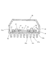
本発明の実施例の一つである照明装置1を図1及び2に示す。図1は照明装置1の斜視図、図2は図1のA−A線位置での断面図である。また、照明装置1に使用されるプリント配線板11の裏面側を図3に示す。照明装置1は例えば車両室内又は室外用の照明に利用される。
照明装置1ではLED実装基板10が筐体30に収納される。LED実装基板10は大別してプリント配線板11、LEDランプ20及びLED駆動用デバイスからなる。プリント配線板11の実装面側には導体パターン(12、13)が形成されている。LEDランプ20と抵抗21の実装領域ができるだけ離間するように導体パターン(12、13)が形成される。この例ではLED実装領域12がプリント配線板11の縁部に配置され、LED駆動用デバイスの中で特に発熱量が大きい抵抗21の実装領域13がプリント配線板11の中心を挟んで反対側の縁部に配置されるように導体パターンを形成し、LEDランプ20と抵抗21との距離を十分にとっている。また、抵抗以外のデバイスについてもLEDランプ20から離れた位置に実装されるような導体パターンとしている。
導体パターンは銅箔の印刷によって形成することができる。但し、導体パターンの材質、形成方法はこの例に限定されるものではない。
尚、導体パターンの表面から筐体内の空気へと放散する熱の量を抑えるために、必要最小限の導体パターンを形成している。
An illuminating device 1 which is one embodiment of the present invention is shown in FIGS. FIG. 1 is a perspective view of the lighting device 1, and FIG. 2 is a cross-sectional view taken along the line AA of FIG. Moreover, the back surface side of the printed
In the lighting device 1, the
The conductor pattern can be formed by printing a copper foil. However, the material and formation method of the conductor pattern are not limited to this example.
In order to suppress the amount of heat dissipated from the surface of the conductor pattern to the air in the housing, the minimum necessary conductor pattern is formed.
プリント配線板11の裏面側には放熱パターン(14、15)が形成されている(図2、図3)。この例では2種類の放熱パターン(第1放熱パターン14と第2放熱パターン15)を形成した。図3に示すように、第1放熱パターン14と第2放熱パターン15はプリント配線板11の中央領域を挟んで左右対称に形成されている。プリント配線板11の裏面においてLED実装領域12に対応する領域が第1放熱パターン14によって被覆され、プリント配線板11の裏面において各LED駆動用デバイスの実装領域13に対応する領域が第2放熱パターン15によって被覆されている。第1放熱パターン14及び第2放熱パターン15の被覆面積はそれぞれ、プリント配線板11の裏面全体の面積の約2/5である。また、第1放熱パターン14と第2放熱パターン15の形状はともに矩形である。
各放熱パターンはプリント配線板11の裏面側表面に銅箔をメッキすることによって形成することができる。但し、放熱パターンの材質、形成方法はこの例に限定されるものではない。
A heat radiation pattern (14, 15) is formed on the back side of the printed wiring board 11 (FIGS. 2 and 3). In this example, two types of heat radiation patterns (first
Each heat radiation pattern can be formed by plating a copper foil on the back surface of the printed
プリント配線板11には複数のサーマルビア(16、17)が備えられている。サーマルビアの一部(符号16)は、導体パターンの中のLED実装領域12と第1放熱パターン14とを接続する。残りのサーマルビア(符号17)は、導体パターンの中のLED駆動用デバイス実装領域13と第2放熱パターン15とを接続する。
The printed
筐体30は基板収納部31及びカバー部32から構成される。基板収納部31は熱伝導率が約1 W/m・Kである、アルミ酸化物で表面被覆されたアルミからなるフィラーを含有したポリエステル系の樹脂からなる。
その裏面側を設置面としてプリント配線板11が基板収納部31の内側壁面31aに設置、固定される。これによって、プリント配線板11の裏面側に形成された第1放熱パターン14と第2放熱パターン15がともに基板収納部31の内側壁面31aに密着した状態となる。プリント配線板11の固定は、接着剤、基板収納部31側に備えた係止爪などによって行われる。
The
The printed
基板収納部31の底部の外側壁面31bの一部はリブ状(フィン状)に突出している。即ち、基板収納部31はその外側壁面にリブ状突起部31cを備える。この実施例では、基板収納部31において、LED実装基板10が収納される領域に対応する部分にのみリブ状突起部31cを設けているが、当該部分以外にもリブ状突起部を設けてもよい。
リブ状突起部31cの高さや間隔等は、放熱効率を考慮して設定することができる。例えばリブ状突起部31cの高さを6mm(筐体肉厚の約3倍)とし、間隔を4mmとする。
A part of the
The height, interval, and the like of the rib-
筐体のカバー部32は透光性の樹脂(例えばポリカーボネート樹脂)からなる。カバー部32を基板収納部31に被せることによって実質的な密閉状態が作り出される。LEDランプ20が通電されると、LEDランプ20の光は当該カバー部32を通って外部に照射する。
The
以上の構成の照明装置1における放熱態様を説明する。まず、駆動に伴ってLEDランプ20から放出された熱は、導体パターン(LED実装部12)に伝導し、続いてサーマルビア16を介して第1放熱パターン14へと伝導する。第1放熱パターン14へ伝導した熱は第1放熱パターン14の表面を介して筐体の基板収納部31へと受け渡される。このようにして基板収納部31へ伝導した熱は、基板収納部31の外側表面より外部に放散する。一方、抵抗21から放出された熱も、導体パターン(LED駆動用デバイス実装部13)、サーマルビア17、及び第2放熱パターン15を介して筐体の基板収納部31へと伝導し、そして基板収納部31の外側表面より外部に放散する。このようにLEDランプ20の熱と抵抗21の熱がそれぞれ個別の放熱経路を通って積極的に筐体の基板収納部31へと伝導する。以上の二つの放熱経路が形成されることによって、効率的な放熱が行われるとともに、抵抗21の熱がLEDランプ20へと伝導することが防止される。尚、基板収納部31を介してLEDランプ20と抵抗21とが接続しているものの、基板収納部31の材質を熱伝導率が 約1 W/m・Kの樹脂としたことによって、第2放熱パターン15より基板収納部31へ伝導した抵抗21の熱の中で、基板収納部31を通って第1放熱パターン14へと伝導する熱の量は多くない。このように本実施例では筐体の材質によって、第2放熱パターン15から第1放熱パターン14への熱伝導、即ち抵抗21の熱がLEDランプ20の放熱経路に伝導してLEDランプ20に影響することを防止している。
A heat radiation mode in the lighting device 1 having the above configuration will be described. First, the heat released from the
一方、筐体の基板収納部31にリブ状突起部31cを備えたことによって、基板収納部31の外側壁面の表面積が増大している。これによって、基板収納部31に伝導したLEDランプ20の熱及び抵抗21の熱をより効率的に放散することが可能となる。しかも、リブ状突起部31cが放熱フィンとして機能し、高い放熱効果が得られる。また、第1放熱パターン14及び第2放熱パターン15の接触部の直下にリブ状突起部31cを配置したことから、第1放熱パターン14及び第2放熱パターン15より伝導した熱がリブ状突起部31cへと直接且つ効率的に伝導することになり、リブ状突起部31cによる放熱作用が良好に発揮される。
On the other hand, the surface area of the outer wall surface of the
照明装置1では、プリント配線板11の実装面には必要最小限の導体パターンのみを形成している。このように構成することでLEDランプ20の熱や抵抗21等の熱が導体パターンの表面から筐体内の空気へと放散することを極力抑えている。これによって筐体内の温度上昇が抑制される。
In the lighting device 1, only the minimum necessary conductor pattern is formed on the mounting surface of the printed
以上のように特有の放熱経路を設けたこと及び導体パターンから筐体内の空気への放熱を抑えたことによって、照明装置1では非常に高い放熱効率を達成でき、筐体内の温度上昇を抑えることができる。従って、LEDランプ20の通電電流を増加させ、高輝度に発光させることができる。つまり、高輝度の光を得るのに適した構造となる。
As described above, by providing a specific heat dissipation path and suppressing heat dissipation from the conductor pattern to the air in the housing, the lighting device 1 can achieve very high heat dissipation efficiency and suppress a temperature rise in the housing. Can do. Therefore, the energization current of the
一方、筐体の基板収納部31が備えるリブ状突起部31cは、放熱効果の増大に対して有効に作用すると同時に基板収納部31の補強の役目もする。つまりリブ状突起部31cが放熱と補強という二つの機能を発揮する。その結果、簡易な構成でありながら高い放熱効果を発揮することが可能な装置となる。また、簡易な構成で高い放熱効果が発揮されることから汎用性も高い装置となる。
On the other hand, the rib-
以上の実施例は本発明の具現化の一例であり、様々な変形、変更が可能である。例えば、プリント配線板11の裏面側に形成した各放熱パターンの形状、被覆面積は、放熱効率等を考慮して任意に設計できる。また、本実施例では第2放熱パターン15を利用して全てのLED駆動用デバイスの熱を放熱することにしたが、LED駆動用デバイス毎(或いは、LED駆動用デバイスをいくつかの組に分けて、組毎)に対応する放熱パターンを設け、各LED駆動用デバイス(各組に含まれるデバイス)の熱が個別の放熱経路で放熱されるように構成してもよい。
また、筐体内の温度上昇を抑えるために、筐体の一部に一又は複数の放熱用の孔を設けてもよい。
The above embodiment is an example of realization of the present invention, and various modifications and changes are possible. For example, the shape and covering area of each heat radiation pattern formed on the back surface side of the printed
Moreover, in order to suppress the temperature rise in the housing, one or a plurality of heat radiation holes may be provided in a part of the housing.
上記の実施例では、第2放熱パターン15から第1放熱パターン14への熱伝導を筐体の材質によって防止することにした。より積極的な熱伝導抑制手段を備えた筐体の例を図4に示す。図4(a)では筐体の基板収納部40の厚さが第1放熱パターン14の接触部と第2放熱パターン15の接触部との間41で薄くなっている。このように筐体の一部を薄肉にして断面積を小さくすればそこでの熱伝導量が減少する。これによって第2放熱パターン15から第1放熱パターン14への熱の受け渡しが抑制される。
一方、図4(b)では第1放熱パターン14の接触部と第2放熱パターン15の接触部との間の位置43で基板収納部42の表面にパルス波形状の凹凸を設けている。これによって第2放熱パターン15より基板収納部42に伝導した熱の一部について熱伝導距離が長くなり、第1放熱パターン14への熱伝導量が減少する。この例では筐体の基板収納部42の内側壁面に凹凸を設けたが、内側壁面に代えて又は加えて外側壁面に凹凸を設けることにしてもよい。また、凹凸の大きさ(長さ、深さ)は任意に設定可能である。
In the above embodiment, heat conduction from the second
On the other hand, in FIG. 4B, pulse wave-shaped irregularities are provided on the surface of the substrate storage portion 42 at a
本発明の他の実施例である照明装置2を図5に示す。図5は照明装置2の断面図であり、上記実施例における図2に相当する。尚、以下の説明において上記実施例と同一の部材には同一の符号を付してその説明を省略する。
照明装置2では筐体の基板収納部44の内側壁面44aにプリント配線板11固定用の一対の突起(45、46)が備えられる。当該突起と基板収納部44の内側壁面44aとによって狭持された状態でプリント配線板11が基板収納部44に固定される。そして突起45は導体パターンの中のLED実装領域12の一部に接触した状態となり、突起46は導体パターンの中のLED駆動用デバイス実装領域13の一部に接触した状態となる。これによって、LEDランプ20の熱の一部は導体パターン(LED実装領域12)を介して基板収納部44へと伝導し、抵抗21の熱の一部も同様に導体パターン(LED駆動用デバイス実装領域13)を介して基板収納部44へと伝導する。このように本実施例の構成では導体パターンの一部から直接、筐体への熱伝導が行われる。換言すれば、放熱経路として導体パターン、サーマルビア、及び放熱パターンを通って筐体に伝熱する放熱経路と、導体パターンから直接筐体に伝熱する放熱経路の二つが利用される。このように放熱経路を増加させたことによって筐体への熱伝導効率が高まり、放熱特性が向上する。
An illuminating device 2 which is another embodiment of the present invention is shown in FIG. FIG. 5 is a cross-sectional view of the illumination device 2 and corresponds to FIG. 2 in the above embodiment. In the following description, the same members as those in the above embodiment are denoted by the same reference numerals, and the description thereof is omitted.
In the lighting device 2, a pair of protrusions (45, 46) for fixing the printed
以上のように、本実施例では導体パターンの一部を筐体の基板収納部44に接触させることにした。つまり、導体パターンの一部を筐体への熱伝導を行う放熱パターン(第3放熱パターン)として利用した。このような機能を発揮する放熱パターン(第3放熱パターン)を別に設けることにしてもよい。また、このような放熱経路を二箇所ではなく、三箇所以上設けることにしてもよい。或いは、一箇所のみ(例えばLEDランプ20の熱に対する放熱経路のみ)設けることにしてもよい。
As described above, in this embodiment, a part of the conductor pattern is brought into contact with the
本発明によれば高い放熱効率のLED装置が提供される。高い放熱効率が達成され、筐体内の温度上昇を抑えることができることから、LED光源の通電電流を増加させ、輝度の向上(光束の増大)を図れる。即ち、本発明の構成は高輝度化に適したものといえる。
本発明の構造は、密閉環境下でLED光源に通電する場合に特に有効であるが、筐体内に熱がこもり、それがLEDの駆動状態に影響を与えるおそれのある状況において広く適用可能である。
According to the present invention, an LED device with high heat dissipation efficiency is provided. Since high heat dissipation efficiency is achieved and temperature rise in the housing can be suppressed, the energization current of the LED light source can be increased, and the luminance can be improved (increased luminous flux). That is, the configuration of the present invention is suitable for increasing the brightness.
The structure of the present invention is particularly effective when the LED light source is energized in a sealed environment, but can be widely applied in situations where heat is trapped in the housing, which may affect the driving state of the LED. .
この発明は、上記発明の実施の形態及び実施例の説明に何ら限定されるものではない。特許請求の範囲の記載を逸脱せず、当業者が容易に想到できる範囲で種々の変形態様もこの発明に含まれる。 The present invention is not limited to the description of the embodiments and examples of the invention described above. Various modifications may be included in the present invention as long as those skilled in the art can easily conceive without departing from the description of the scope of claims.
1、2 照明装置
11 プリント配線板
12 導体パターンのLED実装領域
13 導体パターンのLED駆動用デバイス実装領域
14 第1放熱パターン
15 第2放熱パターン
16、17 サーマルビア
20 LEDランプ
21 抵抗
30 筐体
31、44 筐体の基板収納部
31a、44a 基板収納部の内側壁面
31b 基板収納部の外側壁面
31c リブ状突起部
32 筐体のカバー部
45、46 基板収納部の突起部
DESCRIPTION OF SYMBOLS 1, 2
Claims (6)
LED駆動用デバイスと、
前記LED光源及び前記LED駆動用デバイスが実装されるプリント配線板であって、上面側に形成された導体パターンと、裏面側に形成された第1放熱部及び第2放熱部と、前記導体パターンにおける前記LED光源の実装領域から前記第1放熱部へと熱を伝導する第1伝熱部と、前記導体パターンにおける前記LED駆動用デバイスの実装領域から前記第2放熱部へと熱を伝導する第2伝熱部と、を備えたプリント配線板と、
前記LED光源及び前記LED駆動用デバイスが実装された前記プリント配線板を収納する筐体であって、その内側壁面に対して、前記第1放熱部及び前記第2放熱部が接触した状態で前記プリント配線板が固定されるとともに、前記プリント配線板が固定される領域の外側壁面にリブ状突起部が形成された筐体と、を備えてなるLED装置。 An LED light source;
An LED driving device;
A printed wiring board on which the LED light source and the LED driving device are mounted, a conductor pattern formed on the upper surface side, a first heat radiation portion and a second heat radiation portion formed on the back surface side, and the conductor pattern Conducting heat from the LED light source mounting region to the first heat radiating unit in the first heat transfer unit, and conducting the heat from the LED driving device mounting region in the conductor pattern to the second heat radiating unit A printed wiring board comprising a second heat transfer section;
A housing that houses the printed wiring board on which the LED light source and the LED driving device are mounted, and the first heat radiating portion and the second heat radiating portion are in contact with the inner wall surface thereof. An LED device comprising: a casing on which a printed wiring board is fixed, and a rib-shaped protrusion formed on an outer wall surface of an area where the printed wiring board is fixed.
前記第1放熱部及び前記第2放熱部に加えて、該第3放熱部が接触した状態で前記プリント配線板が前記筐体に固定されている、請求項1〜3のいずれかに記載のLED装置。 A third heat radiating portion is formed on the surface of the printed wiring board,
The said printed wiring board is fixed to the said housing | casing in the state which this 3rd heat radiating part contacted in addition to the said 1st heat radiating part and the said 2nd heat radiating part. LED device.
プリント配線板が固定される領域を内側壁面に備えるとともに、該固定領域の外側壁面にリブ状突起部を備えることを特徴とするLED装置用筐体。 A housing for an LED device that houses a printed wiring board on which an LED light source is mounted,
A housing for an LED device, wherein an area to which a printed wiring board is fixed is provided on an inner wall surface, and a rib-like protrusion is provided on an outer wall surface of the fixing area.
Priority Applications (1)
| Application Number | Priority Date | Filing Date | Title |
|---|---|---|---|
| JP2005191442A JP2007012856A (en) | 2005-06-30 | 2005-06-30 | Led apparatus and housing therefor |
Applications Claiming Priority (1)
| Application Number | Priority Date | Filing Date | Title |
|---|---|---|---|
| JP2005191442A JP2007012856A (en) | 2005-06-30 | 2005-06-30 | Led apparatus and housing therefor |
Publications (2)
| Publication Number | Publication Date |
|---|---|
| JP2007012856A true JP2007012856A (en) | 2007-01-18 |
| JP2007012856A5 JP2007012856A5 (en) | 2007-10-25 |
Family
ID=37750979
Family Applications (1)
| Application Number | Title | Priority Date | Filing Date |
|---|---|---|---|
| JP2005191442A Withdrawn JP2007012856A (en) | 2005-06-30 | 2005-06-30 | Led apparatus and housing therefor |
Country Status (1)
| Country | Link |
|---|---|
| JP (1) | JP2007012856A (en) |
Cited By (13)
| Publication number | Priority date | Publication date | Assignee | Title |
|---|---|---|---|---|
| JP2009064833A (en) * | 2007-09-04 | 2009-03-26 | Toshiba Lighting & Technology Corp | Light-emitting device and lighting device with the same |
| WO2009145109A1 (en) | 2008-05-29 | 2009-12-03 | 電気化学工業株式会社 | Metal base circuit board |
| JP2009295449A (en) * | 2008-06-05 | 2009-12-17 | Toshiba Lighting & Technology Corp | Luminaire |
| JP2010003968A (en) * | 2008-06-23 | 2010-01-07 | Panasonic Electric Works Co Ltd | Light-emitting device |
| JP2012519931A (en) * | 2009-03-05 | 2012-08-30 | アイティーアイ スコットランド リミテッド | Light guide |
| JP2014053603A (en) * | 2012-08-31 | 2014-03-20 | Avago Technologies General Ip (Singapore) Private Ltd | Method and system for dissipating heat in optical communication module |
| CN104134740A (en) * | 2014-07-15 | 2014-11-05 | 华南理工大学 | Structurally integrated LED (Light Emitting Diode) packaging structure |
| JP2015073131A (en) * | 2015-01-05 | 2015-04-16 | ローム株式会社 | Led light emitter and led bulb |
| US9625641B2 (en) | 2009-03-05 | 2017-04-18 | Design Led Products Limited | Light guides |
| US9709721B2 (en) | 2008-10-21 | 2017-07-18 | Design Led Products Limited | Light guides |
| US10054301B2 (en) | 2013-09-18 | 2018-08-21 | Denso Corporation | Lighting device and lighting appliance having the lighting device |
| CN111692573A (en) * | 2019-09-30 | 2020-09-22 | 长城汽车股份有限公司 | Lighting device and vehicle |
| CN114690338A (en) * | 2020-12-30 | 2022-07-01 | 华为技术有限公司 | Transmitting optical module, bidirectional optical module, and optical communication device |
Citations (11)
| Publication number | Priority date | Publication date | Assignee | Title |
|---|---|---|---|---|
| JPH03245586A (en) * | 1990-02-23 | 1991-11-01 | Nec Corp | Optical transmission circuit |
| JPH07131129A (en) * | 1993-11-05 | 1995-05-19 | Nippon Telegr & Teleph Corp <Ntt> | Double-side-mounted multichip module |
| JPH10177068A (en) * | 1996-12-19 | 1998-06-30 | Mitsubishi Electric Corp | Optical vehicle sensor |
| JPH10256677A (en) * | 1997-03-13 | 1998-09-25 | Nec Yonezawa Ltd | Printed board |
| JPH11318695A (en) * | 1998-05-15 | 1999-11-24 | Toshiba Home Techno Corp | Household heater |
| JP2001168560A (en) * | 1999-12-07 | 2001-06-22 | Denso Corp | Electronic circuit unit |
| JP2001298290A (en) * | 2000-04-13 | 2001-10-26 | Yazaki Corp | Heat radiation structure of electronic unit box |
| JP2003165773A (en) * | 2001-11-29 | 2003-06-10 | Kyocera Corp | High dielectric constant glass ceramic and wiring board using the same |
| JP2003178602A (en) * | 2001-12-10 | 2003-06-27 | Koito Mfg Co Ltd | Lighting system |
| JP2003258465A (en) * | 2002-03-04 | 2003-09-12 | Denso Corp | Electronic circuit unit |
| JP2005150408A (en) * | 2003-11-17 | 2005-06-09 | Sumitomo Electric Ind Ltd | Light source apparatus and package for mounting light emitting element |
-
2005
- 2005-06-30 JP JP2005191442A patent/JP2007012856A/en not_active Withdrawn
Patent Citations (11)
| Publication number | Priority date | Publication date | Assignee | Title |
|---|---|---|---|---|
| JPH03245586A (en) * | 1990-02-23 | 1991-11-01 | Nec Corp | Optical transmission circuit |
| JPH07131129A (en) * | 1993-11-05 | 1995-05-19 | Nippon Telegr & Teleph Corp <Ntt> | Double-side-mounted multichip module |
| JPH10177068A (en) * | 1996-12-19 | 1998-06-30 | Mitsubishi Electric Corp | Optical vehicle sensor |
| JPH10256677A (en) * | 1997-03-13 | 1998-09-25 | Nec Yonezawa Ltd | Printed board |
| JPH11318695A (en) * | 1998-05-15 | 1999-11-24 | Toshiba Home Techno Corp | Household heater |
| JP2001168560A (en) * | 1999-12-07 | 2001-06-22 | Denso Corp | Electronic circuit unit |
| JP2001298290A (en) * | 2000-04-13 | 2001-10-26 | Yazaki Corp | Heat radiation structure of electronic unit box |
| JP2003165773A (en) * | 2001-11-29 | 2003-06-10 | Kyocera Corp | High dielectric constant glass ceramic and wiring board using the same |
| JP2003178602A (en) * | 2001-12-10 | 2003-06-27 | Koito Mfg Co Ltd | Lighting system |
| JP2003258465A (en) * | 2002-03-04 | 2003-09-12 | Denso Corp | Electronic circuit unit |
| JP2005150408A (en) * | 2003-11-17 | 2005-06-09 | Sumitomo Electric Ind Ltd | Light source apparatus and package for mounting light emitting element |
Cited By (15)
| Publication number | Priority date | Publication date | Assignee | Title |
|---|---|---|---|---|
| JP2009064833A (en) * | 2007-09-04 | 2009-03-26 | Toshiba Lighting & Technology Corp | Light-emitting device and lighting device with the same |
| WO2009145109A1 (en) | 2008-05-29 | 2009-12-03 | 電気化学工業株式会社 | Metal base circuit board |
| US8426740B2 (en) | 2008-05-29 | 2013-04-23 | Denki Kagaku Kogyo Kabushiki Kaisha | Metal base circuit board |
| JP2009295449A (en) * | 2008-06-05 | 2009-12-17 | Toshiba Lighting & Technology Corp | Luminaire |
| JP2010003968A (en) * | 2008-06-23 | 2010-01-07 | Panasonic Electric Works Co Ltd | Light-emitting device |
| US9709721B2 (en) | 2008-10-21 | 2017-07-18 | Design Led Products Limited | Light guides |
| US9164223B2 (en) | 2009-03-05 | 2015-10-20 | Iti Scotland Limited | Light guides |
| US9625641B2 (en) | 2009-03-05 | 2017-04-18 | Design Led Products Limited | Light guides |
| JP2012519931A (en) * | 2009-03-05 | 2012-08-30 | アイティーアイ スコットランド リミテッド | Light guide |
| JP2014053603A (en) * | 2012-08-31 | 2014-03-20 | Avago Technologies General Ip (Singapore) Private Ltd | Method and system for dissipating heat in optical communication module |
| US10054301B2 (en) | 2013-09-18 | 2018-08-21 | Denso Corporation | Lighting device and lighting appliance having the lighting device |
| CN104134740A (en) * | 2014-07-15 | 2014-11-05 | 华南理工大学 | Structurally integrated LED (Light Emitting Diode) packaging structure |
| JP2015073131A (en) * | 2015-01-05 | 2015-04-16 | ローム株式会社 | Led light emitter and led bulb |
| CN111692573A (en) * | 2019-09-30 | 2020-09-22 | 长城汽车股份有限公司 | Lighting device and vehicle |
| CN114690338A (en) * | 2020-12-30 | 2022-07-01 | 华为技术有限公司 | Transmitting optical module, bidirectional optical module, and optical communication device |
Similar Documents
| Publication | Publication Date | Title |
|---|---|---|
| JP2007012856A (en) | Led apparatus and housing therefor | |
| JP3965929B2 (en) | LED lighting device | |
| JP4757174B2 (en) | Backlight unit | |
| KR100818745B1 (en) | LED module having cooling apparatus | |
| JP4337310B2 (en) | LED lighting device | |
| US20090141508A1 (en) | Lamp with heat conducting structure and lamp cover thereof | |
| JP4969332B2 (en) | Substrate and lighting device | |
| EP2723153A2 (en) | Electronic unit | |
| WO1986002985A1 (en) | Signal light unit having heat dissipating function | |
| RU2546492C1 (en) | Semiconductor device with cooling | |
| KR20080088890A (en) | Light emitting diode bulb having heat dissipation | |
| JP2018029037A (en) | Vehicular lighting system and vehicular lighting tool | |
| JP2008041638A (en) | Heat dissipation device for backlight light source for flat panel display | |
| JP2006331858A (en) | Lighting system | |
| JP2005109228A (en) | Led device and led illumination apparatus | |
| JP2010198952A (en) | Led lighting device | |
| JP2012256677A (en) | Light-emitting device | |
| KR101393052B1 (en) | Ceramic separation type led lighting apparatus having high radiation | |
| JP5835560B2 (en) | Lighting device | |
| JP2006147333A (en) | Led-mounting printed circuit board | |
| JP2001044517A (en) | Light emitter | |
| KR101188350B1 (en) | Light Emitting Diode Lamp using Heat Spreader | |
| JP2016225323A (en) | Light source unit and vehicle headlamp using the same | |
| JP2009224664A (en) | Heat radiating structure | |
| JP6098457B2 (en) | Lighting device and lamp provided with the lighting device |
Legal Events
| Date | Code | Title | Description |
|---|---|---|---|
| A521 | Written amendment |
Free format text: JAPANESE INTERMEDIATE CODE: A523 Effective date: 20070830 |
|
| A621 | Written request for application examination |
Free format text: JAPANESE INTERMEDIATE CODE: A621 Effective date: 20071024 |
|
| A977 | Report on retrieval |
Free format text: JAPANESE INTERMEDIATE CODE: A971007 Effective date: 20100813 |
|
| A131 | Notification of reasons for refusal |
Free format text: JAPANESE INTERMEDIATE CODE: A131 Effective date: 20100825 |
|
| A761 | Written withdrawal of application |
Free format text: JAPANESE INTERMEDIATE CODE: A761 Effective date: 20100929 |