JP2006147333A - Led-mounting printed circuit board - Google Patents
Led-mounting printed circuit board Download PDFInfo
- Publication number
- JP2006147333A JP2006147333A JP2004335496A JP2004335496A JP2006147333A JP 2006147333 A JP2006147333 A JP 2006147333A JP 2004335496 A JP2004335496 A JP 2004335496A JP 2004335496 A JP2004335496 A JP 2004335496A JP 2006147333 A JP2006147333 A JP 2006147333A
- Authority
- JP
- Japan
- Prior art keywords
- region
- circuit board
- printed circuit
- led
- cover
- Prior art date
- Legal status (The legal status is an assumption and is not a legal conclusion. Google has not performed a legal analysis and makes no representation as to the accuracy of the status listed.)
- Withdrawn
Links
Images
Abstract
Description
本発明はLED実装用プリント基板及びそれを利用したLED照明装置に関する。 The present invention relates to a printed circuit board for LED mounting and an LED lighting device using the same.
高輝度、長寿命等の利点を有するLEDが照明装置の光源として使用されつつある。このような背景の中で、LEDを用いた照明装置のさらなる高輝度化が要請されている。ところで、通常、電流量を増加させればLEDの輝度は上昇する。しかし、電流量を増加されせばそれに伴いLEDの制御回路からの発熱も増加し、その影響を受けてLEDが損傷する恐れがある。そのため、高放熱基板を用いることで熱的緩和を図るのが一般的であった。 LEDs having advantages such as high brightness and long life are being used as light sources for lighting devices. In such a background, there is a demand for further increasing the brightness of lighting devices using LEDs. By the way, normally, if the amount of current is increased, the luminance of the LED increases. However, if the amount of current is increased, the heat generated from the LED control circuit increases accordingly, and the LED may be damaged under the influence. For this reason, it has been common to achieve thermal relaxation by using a high heat dissipation substrate.
しかし、高放熱基板を用いると製造コストが上昇する。また、部品実装上も片面実装となり基板のサイズを大きくせざるを得ない。
そこで、本発明は製造コストの低減を図れるとともに、部品実装上の制約も少なく、さらにサイズ面でも有利なLED実装用のプリント基板を提供することを目的とする。
However, the use of a high heat dissipation substrate increases the manufacturing cost. In addition, component mounting is also one-sided mounting, and the size of the board must be increased.
SUMMARY OF THE INVENTION An object of the present invention is to provide a printed circuit board for LED mounting that can reduce the manufacturing cost, has few restrictions on component mounting, and is advantageous in terms of size.
本発明は上記課題の少なくとも一つを解決するために次の構成からなる。すなわち、
LEDが実装される第1領域と、
前記LEDの制御回路を構成する要素のうちの発熱要素が実装される第2領域と、
前記第2領域で発生した熱の伝導を制限するために前記第1領域と前記第2領域との間に形成されるスリット状貫通孔と、
を備えるプリント基板である。
The present invention comprises the following configuration in order to solve at least one of the above problems. That is,
A first region where the LED is mounted;
A second region in which a heating element among the elements constituting the LED control circuit is mounted;
A slit-shaped through hole formed between the first region and the second region to limit conduction of heat generated in the second region;
Is a printed circuit board.
上記構成では、プリント基板は、LEDが実装される第1領域と、制御回路が実装される第2領域とに分けられ、これらの領域の境界にスリット状貫通孔が形成される。このようにスリット状貫通孔によって第1領域と第2領域とを一部において分断したことから、第2領域で発生した熱が第1領域に伝導されることを効果的に制限することができる。すなわち、第1領域に実装されたLEDは、第2領域の制御回路で発生した熱の影響を受けにくい。
以上のように、スリット状貫通孔を設けるという簡易な構造によって、実装されたLEDへの熱的影響を格段に減少させることができるプリント基板となる。したがって、コストが低減され、部品実装上の制約が少なくなり、さらにサイズ面でも有利なプリント基板を実現できる。
In the above configuration, the printed circuit board is divided into a first region where the LED is mounted and a second region where the control circuit is mounted, and a slit-shaped through hole is formed at the boundary between these regions. As described above, since the first region and the second region are partly divided by the slit-shaped through hole, it is possible to effectively limit the heat generated in the second region from being conducted to the first region. . That is, the LED mounted in the first area is not easily affected by the heat generated by the control circuit in the second area.
As described above, with a simple structure in which the slit-shaped through hole is provided, a printed circuit board that can significantly reduce the thermal influence on the mounted LED is obtained. Therefore, it is possible to realize a printed circuit board that is reduced in cost, has fewer restrictions on component mounting, and is advantageous in terms of size.
以下、本発明の構成要素について説明する。 Hereinafter, the components of the present invention will be described.
(プリント基板及びスリット状貫通孔)
プリント基板はLED及びその制御回路を実装するために用いられる。材質は特に限定されないが、例えば、フェノール系樹脂、エポキシ系樹脂等が使用される。
プリント基板は第1領域と第2領域とを備える。第1領域にはLED等の発光素子が実装される。第2領域には発光素子の制御回路を構成する要素のうち少なくとも発熱要素(抵抗、トランジスタ、ダイオード等)が実装される。制御回路の全構成要素を第2領域に実装してもよい。また、発熱要素であっても制御回路の特性上、発光素子の近傍に配置せざるを得ないものは第1領域に実装される。
第2領域で発生した熱がプリント基板を介して、直接第1領域へ伝導しLEDに影響を与えることを回避するため、第1領域と第2領域との境界にスリット状貫通孔を設ける。これにより、第2領域で発生した熱の第1領域に対する伝導が制限される。すなわち、LEDが熱による影響を受けることを低減できる。一方、スリット状貫通孔を形成した場合、第2領域で発生した熱の一部は第1領域と第2領域との連続した部分より伝導されることが予想される。しかし、第2領域から第1領域への経路長が長くなるため、経路長の長さに比例して放熱量も増加し、最終的に第1領域に到達する熱量は少なくなる。よって、LEDは熱の影響を受けにくい。
(Printed circuit board and slit-shaped through hole)
The printed circuit board is used for mounting the LED and its control circuit. Although the material is not particularly limited, for example, a phenol resin, an epoxy resin, or the like is used.
The printed circuit board includes a first region and a second region. A light emitting element such as an LED is mounted in the first region. In the second region, at least heating elements (resistors, transistors, diodes, etc.) among the elements constituting the control circuit of the light emitting element are mounted. All components of the control circuit may be mounted in the second region. Moreover, even if it is a heat generating element, what must be arrange | positioned in the vicinity of a light emitting element on the characteristic of a control circuit is mounted in a 1st area | region.
In order to avoid the heat generated in the second region from being directly conducted to the first region via the printed circuit board and affecting the LED, a slit-shaped through hole is provided at the boundary between the first region and the second region. This limits the conduction of heat generated in the second region to the first region. That is, it is possible to reduce the LED from being affected by heat. On the other hand, when the slit-shaped through hole is formed, it is expected that part of the heat generated in the second region is conducted from a continuous portion of the first region and the second region. However, since the path length from the second area to the first area becomes longer, the heat radiation amount increases in proportion to the length of the path length, and the amount of heat finally reaching the first area decreases. Therefore, the LED is not easily affected by heat.
LEDと発熱要素とを結ぶ仮想直線がスリット状貫通孔上を通過するように、スリット状貫通孔を形成することが好ましい。スリット状貫通孔の長辺の長さは、第2領域で発生した熱を制限するために、できるだけ長いことが好ましい。ただし、プリント基板の十分な強度が確保できるとともに、配線上問題がないようにスリットの長さを設定する。例えば、スリット状貫通孔の長辺の長さは、第1領域と第2領域との境界の70%以上にすることが好ましい。さらに好ましくは80%以上である。境界に対する長さの上限は特に限定されないが、例えば、90%である。 It is preferable to form the slit-shaped through hole so that a virtual straight line connecting the LED and the heat generating element passes over the slit-shaped through hole. The length of the long side of the slit-shaped through hole is preferably as long as possible in order to limit the heat generated in the second region. However, the length of the slit is set so that sufficient strength of the printed circuit board can be secured and there is no problem in wiring. For example, the length of the long side of the slit-like through hole is preferably 70% or more of the boundary between the first region and the second region. More preferably, it is 80% or more. Although the upper limit of the length with respect to a boundary is not specifically limited, For example, it is 90%.
プリント基板内の熱を効率的に放熱させるため、プリント基板の表面の一部に放熱パターンを形成することが好ましい。特に第1領域に実装されるLEDへの熱的影響を低減するために、第1領域の表面に放熱パターンを形成するが好ましい。放熱パターンの材質は特に限定されない。材質の例としては銅を挙げることができる。より効率的に放熱するためにプリント基板の裏面にも放熱パターンを形成することが好ましい。放熱パターンはLED実装面及び裏面ともに第1領域の30%以上であることが好ましい。さらに、好ましくは50%以上である。放熱パターンを形成する領域の上限は特に限定されないが、約90%である。 In order to efficiently dissipate the heat in the printed circuit board, it is preferable to form a heat radiation pattern on a part of the surface of the printed circuit board. In particular, in order to reduce the thermal influence on the LED mounted in the first region, it is preferable to form a heat radiation pattern on the surface of the first region. The material of the heat radiation pattern is not particularly limited. An example of the material is copper. In order to dissipate heat more efficiently, it is preferable to form a heat dissipation pattern on the back surface of the printed circuit board. The heat dissipating pattern is preferably 30% or more of the first region on both the LED mounting surface and the back surface. Furthermore, it is preferably 50% or more. The upper limit of the region for forming the heat radiation pattern is not particularly limited, but is about 90%.
(LED)
LEDは照明用光源として用いられる。LEDの種類は特に限定されないが、例えば、レンズ形状の封止部材を有する砲弾タイプやSMDタイプ(表面実装型)の素子を用いる。LEDの発光色も特に限定されず、例えば、白色LEDを使用することができる。
(LED)
The LED is used as an illumination light source. The type of LED is not particularly limited. For example, a bullet type or SMD type (surface mount type) element having a lens-shaped sealing member is used. The emission color of the LED is not particularly limited, and for example, a white LED can be used.
(制御回路)
制御回路はLEDの動作状態を制御するために用いられる。具体的には例えば、LEDに流れる電流を一定に制御するために制御回路が用いられる。制御回路を構成する素子としては例えば、抵抗、トランジスタ等が使用される。それらの素子は、電流量を増加させた場合の発熱量が大きく、その熱はプリント基板内を伝導してLEDを損傷する恐れがある。そこで、本発明では、上記の通りプリント基板に形成されたスリット状貫通孔を利用して、制御回路を構成する素子(発熱要素)からの熱の伝導を積極的に抑制する。
(Control circuit)
The control circuit is used to control the operating state of the LED. Specifically, for example, a control circuit is used to control the current flowing through the LED to be constant. For example, a resistor, a transistor, or the like is used as an element constituting the control circuit. These elements generate a large amount of heat when the amount of current is increased, and the heat may be conducted through the printed circuit board to damage the LED. Therefore, in the present invention, the conduction of heat from the elements (heat generating elements) constituting the control circuit is positively suppressed using the slit-shaped through holes formed in the printed board as described above.
(カバー)
カバーはプリント基板とともに使用されて照明装置を構成する。また、外部との接触を防止する役割も有する。カバーは、プリント基板を覆うようにLEDの外表面側に取付られる。カバーの材質は特に限定されず、例えば、ポリカーボネート樹脂、アクリル樹脂等を使用することができる。
カバーの外表面の一部を凸レンズ状にし、カバーにレンズ効果を付与することもできる。この構成により、LEDの光がカバーを通過する際に収れんされる。このようなカバーに形成されるレンズに加えて、又はこれとは別にレンズを使用してLEDの光を制御してもよい。
(cover)
The cover is used together with a printed circuit board to constitute a lighting device. It also has a role of preventing contact with the outside. The cover is attached to the outer surface side of the LED so as to cover the printed board. The material of the cover is not particularly limited, and for example, a polycarbonate resin, an acrylic resin, or the like can be used.
A part of the outer surface of the cover can be formed into a convex lens shape to give a lens effect to the cover. With this configuration, the light from the LED is converged when passing through the cover. In addition to or in addition to the lens formed on such a cover, a lens may be used to control the light of the LED.
特にプリント基板をカバーで覆った場合には第2領域で発生した熱がプリント基板の上方の空間を介して第1領域へと伝導する恐れがある。そこで、カバーのプリント基板側に遮へい板を形成し、その遮へい板の先端がプリント基板の第1領域と第2領域との境界又は境界近傍に接するように形成することが好ましい。これにより、空間を介して第1領域へ伝導する熱を制限することができるため、LEDは熱的影響を受けにくくなる。
なお、遮へい板の材質は、特に限定されない。カバーと遮へい板は一体成型した場合は、遮へい板の材質はカバーと同じとなる。
In particular, when the printed circuit board is covered with a cover, the heat generated in the second region may be conducted to the first region through the space above the printed circuit board. Therefore, it is preferable to form a shielding plate on the printed circuit board side of the cover and to make the tip of the shielding plate come into contact with or near the boundary between the first region and the second region of the printed circuit board. Thereby, since heat conducted to the first region through the space can be limited, the LED is not easily affected by heat.
In addition, the material of a shielding board is not specifically limited. When the cover and the shielding plate are integrally molded, the material of the shielding plate is the same as that of the cover.
上述のようにプリント基板をカバーで覆って、第1領域と第2領域の境界又は境界近傍に、先端がプリント基板に接する遮へい板を形成した場合、第1領域の上方の空間と第2領域の上方の空間がともに密封状態が高くなる。特にスリット状貫通孔が遮へい板により塞がれる場合には実質的な密封状態となる。この空間にプリント基板から空間中に排出された熱が充満され、LEDに熱的影響を及ぼす。そのため、プリント基板の第1領域と第2領域ともに通気孔を形成することが好ましい。 When the shielding board whose tip is in contact with the printed circuit board is formed at or near the boundary between the first area and the second area by covering the printed circuit board with the cover as described above, the space above the first area and the second area Both of the spaces above are highly sealed. In particular, when the slit-shaped through hole is blocked by a shielding plate, a substantially sealed state is obtained. This space is filled with the heat discharged from the printed circuit board into the space, and the LED is thermally affected. Therefore, it is preferable to form a vent hole in both the first region and the second region of the printed circuit board.
カバーは、本発明の一態様ではプリント基板に固定される。固定方法として、ねじを使用する場合、カバーの一部にねじ孔を形成するとともに、プリント基板の対応する位置にもねじ孔を形成する。ここで、ねじ孔の一部としてスリット状貫通孔を利用することが好ましい。これにより、別途ねじ孔を形成する手間が省ける。また、限られたプリント基板内を有効に活用することができる。 The cover is fixed to the printed board in one embodiment of the present invention. When a screw is used as a fixing method, a screw hole is formed in a part of the cover, and a screw hole is also formed at a corresponding position on the printed board. Here, it is preferable to use a slit-like through hole as a part of the screw hole. Thereby, the trouble of forming a separate screw hole can be saved. In addition, the limited printed circuit board can be used effectively.
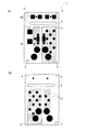
図1は本発明の実施例であるプリント基板1の平面図である。図1(a)はプリント基板1のLED実装面側の図であり、(b)はプリント基板1の裏面側の図である。プリント基板1はLED照明装置に使用され、LED及びその制御回路が実装される。
プリント基板1は第1領域10と第2領域20とを備える。第1領域10と第2領域20との境界にスリット状貫通孔2が形成されている。LEDは第1領域10のA−A上に実装される。プリント基板1は両面銅張りの積層板である。
FIG. 1 is a plan view of a printed circuit board 1 according to an embodiment of the present invention. FIG. 1A is a diagram of the printed circuit board 1 on the LED mounting surface side, and FIG. 1B is a diagram of the back surface side of the printed circuit board 1. The printed circuit board 1 is used in an LED lighting device, and an LED and its control circuit are mounted.
The printed circuit board 1 includes a
プリント基板1は第1領域10と第2領域20とを備える。第1領域10にはLED等の素子が実装される。第2領域20には制御回路(抵抗)の素子が実装される。第2領域20で発生した熱がプリント基板1を介して直接第1領域10へと伝導し、LEDに影響を与えることを回避するため、第1領域10と第2領域20との境界にスリット状貫通孔2を設ける。これにより、第2領域20で発生した熱の第1領域10に対する伝導を制限できる。すなわち、LEDが基板から伝わる発熱要素による熱の影響を受けることを低減できる。一方、スリット状貫通孔2を形成した場合、第2領域20で発生した熱の一部は第1領域10と第2領域20との連続した部分より伝導されると予想される。しかし、第2領域20から第1領域10への経路長が長くなるため、経路長の長さに比例して放熱量は増加し、最終的に第1領域に到達する熱量は少なくなる。
この実施例では第1領域10の面積は第2領域20の面積の4倍である。これにより、第1領域10で発生した熱及び第2領域20から第1領域10へ伝導される熱は、第1領域10の表面より効率的に放熱される。
さらに、第1領域10には放熱パターン3を形成することで効率的に放熱させることができる。特にLEDを含む領域に放熱パターン3を形成することにより、LEDへの熱の影響を低減できる。裏面側にも同様な放熱パターン3を形成し、より効率的に放熱させることができる。この実施例ではLED実装面及び裏面のパターン3の面積は第1領域10の面積の60%である。
The printed circuit board 1 includes a
In this embodiment, the area of the
Further, the
以上のような構成により、第1領域10と第2領域20との境界にスリット状貫通孔2を形成することにより、第2領域20から第1領域10までの経路長を長くすることができる。そのため、プリント基板1の第1領域10にLEDを実装し、第2領域20に発熱素子(抵抗)を実装することで、電流量を増加したとしても、LEDは熱的影響を受けにくい。すなわち、コストが低減され、部品実装上の制約がなくなり、さらにサイズ面でも有利なプリント基板を実現できる。
With the configuration as described above, by forming the slit-like through
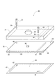
図2に本発明における他の実施例であるLED照明装置30の分解斜視図を示す。LED照明装置30はプリント基板36のLED実装面側にカバー31が取付けられ、カバー31とプリント基板36がねじ33を用いて取付面41へと固定される。LED38は第1領域100に実装される。LED38としてSMDタイプの白色LEDが使用される。LED照明装置30は車両内における照明に使用される。
なお、プリント基板36は上記実施例と同様であるためその説明を省略する。
FIG. 2 shows an exploded perspective view of an
Since the printed
カバー31はプリント基板36とともに使用されLED照明装置30を構成する。また、カバー31はプリント基板36と外部との接触を防止する役割も有する。カバー31の材質はポリカーボネート樹脂である。
カバー31の外表面にはプリント基板10のLED実装部の直上領域が凸レンズ状に形成されている。この構成によりLED38の光がカバーを通過する際に収れんされ、所望の範囲を照射する光が生成される。
プリント基板36はカバー31により覆われるため、第2領域200で発生した熱がプリント基板36の上方の空間を介して第1領域100へと伝導する恐れがある。そこで、カバー31において、第1領域100と第2領域200の境界又は境界近傍の上方に、先端がプリント基板36に接する遮へい板34を形成する。これにより、空間を介して第1領域100へ伝導する熱を制限することができるため、LED38は熱的影響を受けにくくなる。なお、遮へい板34の材質はカバーと同じ材質のポリカーボネート樹脂である。
プリント基板36をカバー31で覆って、第1領域100と第2領域200の境界又は境界近傍に、先端がプリント基板36に接する遮へい板34を形成すると、第1領域100の上方の空間と第2領域200の上方の空間とがともに密封状態が高くなる。この空間にプリント基板36の表面から放出された熱が充満され、LED38に熱的影響を及ぼす恐れがある。そのため、プリント基板36の第1領域100と第2領域200にそれぞれ通気孔39を設けている。
The
A region directly above the LED mounting portion of the printed
Since the printed
When the shielding
カバー31及びプリント基板36を固定するためにねじ33を用いる。そのため、カバー31の一部にねじ孔35を形成するとともに、プリント基板36の対応する位置にもねじ孔40を形成する。また、プリント基板36の製造工程を削減し、プリント基板36内を有効に活用するため、スリット状貫通孔37の一部をねじ孔として利用することとした。
取付面41には、カバー31及びプリント基板36を固定するためのねじ孔42を設けておく。また、車体内部からLED照明装置30への配線、及びプリント基板36で生じた熱を放熱させるために開口部43を形成する。
A
上記のように構成されるLED照明装置30は車両内の照明用として使用される。車両内の壁面に開口部を形成し、LED照明装置30を固定するためのねじ孔を形成する。LED照明装置30の電気配線を行った後に、LED照明装置30をねじにより固定することとなる。
カバー31の外表面が凸レンズ状に形成されているため、所望の距離にLEDの光が収れんされる。従って、車両内照明におけるマップランプ等として好適に利用できる。
The
Since the outer surface of the
以上のような構成により、プリント基板で生じた熱は効率的に外部へと放熱される。そのため、LEDへの電流を増加させたとしても、LEDは熱的影響を受けにくい。よって、本構成においてもLEDの高輝度化を実現できる。 With the above configuration, the heat generated in the printed circuit board is efficiently radiated to the outside. Therefore, even if the current to the LED is increased, the LED is not easily affected by heat. Therefore, high brightness of the LED can be realized also in this configuration.
この発明は上記発明の実施の態様及び実施例の説明に何ら限定されるものではない。特許請求の範囲を逸脱せず、当業者が容易に想到できる範囲で種々の変形態様もこの発明に含まれる。 The present invention is not limited to the description of the embodiments and examples of the invention described above. Various modifications are also included in the present invention as long as those skilled in the art can easily conceive without departing from the scope of the claims.
1 36 プリント基板
2 37 スリット状貫通孔
3 放熱用パターン
10 100 第1領域
20 200 第2領域
30 LED照明装置
31 カバー
34 遮へい板
DESCRIPTION OF SYMBOLS 1 36 Printed
Claims (10)
前記LEDの制御回路を構成する要素のうちの発熱要素が実装される第2領域と、
前記第2領域で発生した熱の伝導を制限するために前記第1領域と前記第2領域との間に形成されるスリット状貫通孔と、
を備えるプリント基板。 A first region where the LED is mounted;
A second region in which a heating element among the elements constituting the LED control circuit is mounted;
A slit-shaped through hole formed between the first region and the second region to limit conduction of heat generated in the second region;
Printed circuit board.
前記プリント基板に実装されたLED及び制御回路と、
前記プリント基板のLED実装面側を覆うように取付られるカバーと、
を備えるLED照明装置。 A printed circuit board according to any one of claims 1 to 5,
An LED and a control circuit mounted on the printed circuit board;
A cover attached to cover the LED mounting surface side of the printed circuit board;
LED lighting device comprising:
The heat dissipation vent is formed in the printed circuit board in order to discharge heat generated in the space surrounded by the cover and the printed circuit board. LED lighting device.
Priority Applications (1)
| Application Number | Priority Date | Filing Date | Title |
|---|---|---|---|
| JP2004335496A JP2006147333A (en) | 2004-11-19 | 2004-11-19 | Led-mounting printed circuit board |
Applications Claiming Priority (1)
| Application Number | Priority Date | Filing Date | Title |
|---|---|---|---|
| JP2004335496A JP2006147333A (en) | 2004-11-19 | 2004-11-19 | Led-mounting printed circuit board |
Publications (2)
| Publication Number | Publication Date |
|---|---|
| JP2006147333A true JP2006147333A (en) | 2006-06-08 |
| JP2006147333A5 JP2006147333A5 (en) | 2007-02-15 |
Family
ID=36626774
Family Applications (1)
| Application Number | Title | Priority Date | Filing Date |
|---|---|---|---|
| JP2004335496A Withdrawn JP2006147333A (en) | 2004-11-19 | 2004-11-19 | Led-mounting printed circuit board |
Country Status (1)
| Country | Link |
|---|---|
| JP (1) | JP2006147333A (en) |
Cited By (9)
| Publication number | Priority date | Publication date | Assignee | Title |
|---|---|---|---|---|
| EP1881362A1 (en) * | 2006-07-21 | 2008-01-23 | Sony Corporation | Light source module, light source apparatus and liquid crystal display |
| JP2008180633A (en) * | 2007-01-25 | 2008-08-07 | Alps Electric Co Ltd | Substrate for sensor element |
| JP2013188243A (en) * | 2012-03-12 | 2013-09-26 | Kpe Inc | Game machine |
| JP2014086241A (en) * | 2012-10-23 | 2014-05-12 | Stanley Electric Co Ltd | LED lamp |
| CN104488077A (en) * | 2014-06-23 | 2015-04-01 | 华为技术有限公司 | Chip heat dissipation structure and terminal device |
| WO2015098383A1 (en) | 2013-12-26 | 2015-07-02 | 岩崎電気株式会社 | Led lamp |
| US9750133B2 (en) | 2015-03-12 | 2017-08-29 | Kabushiki Kaisha Toshiba | Printed circuit board |
| JP2018046058A (en) * | 2016-09-12 | 2018-03-22 | 矢崎総業株式会社 | Electronic circuit board |
| WO2023203750A1 (en) * | 2022-04-22 | 2023-10-26 | 日立Astemo株式会社 | Electronic control device |
-
2004
- 2004-11-19 JP JP2004335496A patent/JP2006147333A/en not_active Withdrawn
Cited By (10)
| Publication number | Priority date | Publication date | Assignee | Title |
|---|---|---|---|---|
| EP1881362A1 (en) * | 2006-07-21 | 2008-01-23 | Sony Corporation | Light source module, light source apparatus and liquid crystal display |
| US7878680B2 (en) | 2006-07-21 | 2011-02-01 | Sony Corporation | Light source module, light source apparatus and liquid crystal display |
| JP2008180633A (en) * | 2007-01-25 | 2008-08-07 | Alps Electric Co Ltd | Substrate for sensor element |
| JP2013188243A (en) * | 2012-03-12 | 2013-09-26 | Kpe Inc | Game machine |
| JP2014086241A (en) * | 2012-10-23 | 2014-05-12 | Stanley Electric Co Ltd | LED lamp |
| WO2015098383A1 (en) | 2013-12-26 | 2015-07-02 | 岩崎電気株式会社 | Led lamp |
| CN104488077A (en) * | 2014-06-23 | 2015-04-01 | 华为技术有限公司 | Chip heat dissipation structure and terminal device |
| US9750133B2 (en) | 2015-03-12 | 2017-08-29 | Kabushiki Kaisha Toshiba | Printed circuit board |
| JP2018046058A (en) * | 2016-09-12 | 2018-03-22 | 矢崎総業株式会社 | Electronic circuit board |
| WO2023203750A1 (en) * | 2022-04-22 | 2023-10-26 | 日立Astemo株式会社 | Electronic control device |
Similar Documents
| Publication | Publication Date | Title |
|---|---|---|
| EP2723153A2 (en) | Electronic unit | |
| JP2008098020A (en) | Led lighting device | |
| JP4337310B2 (en) | LED lighting device | |
| JP2010153044A (en) | Light source unit and luminaire | |
| KR100898817B1 (en) | Light emitting diode bulb having heat dissipation | |
| JP2007012856A (en) | Led apparatus and housing therefor | |
| JP2009301810A (en) | Illuminating device | |
| JP2009004129A (en) | Substrate, and illumination device | |
| JP2006147333A (en) | Led-mounting printed circuit board | |
| JP2010153048A (en) | Light source unit and luminaire | |
| JP2006331858A (en) | Lighting system | |
| JP5278656B2 (en) | Display device | |
| KR100791594B1 (en) | Illuminator having radiating unit | |
| KR101479635B1 (en) | A high power type led lighing device | |
| US20150201486A1 (en) | Stacked Heatsink Assembly | |
| JP6593587B2 (en) | VEHICLE LIGHTING DEVICE AND VEHICLE LIGHT | |
| JP2017174675A (en) | Illumination tool | |
| JP2017174671A (en) | Illumination tool | |
| JP2017224466A (en) | Vehicle lighting device and vehicle lamp fitting | |
| JP2017168274A (en) | Vehicular lighting device and vehicular lighting fixture | |
| JP2010251191A (en) | Projector | |
| JP6569866B2 (en) | lighting equipment | |
| JP2017174780A (en) | Lamp device and luminaire | |
| JP2011108471A (en) | Light source device and equipment | |
| JP6861383B2 (en) | lighting equipment |
Legal Events
| Date | Code | Title | Description |
|---|---|---|---|
| A521 | Written amendment |
Free format text: JAPANESE INTERMEDIATE CODE: A523 Effective date: 20061226 |
|
| A621 | Written request for application examination |
Free format text: JAPANESE INTERMEDIATE CODE: A621 Effective date: 20070125 |
|
| A977 | Report on retrieval |
Free format text: JAPANESE INTERMEDIATE CODE: A971007 Effective date: 20090213 |
|
| A131 | Notification of reasons for refusal |
Free format text: JAPANESE INTERMEDIATE CODE: A131 Effective date: 20090217 |
|
| A761 | Written withdrawal of application |
Free format text: JAPANESE INTERMEDIATE CODE: A761 Effective date: 20090331 |