JP5835560B2 - Lighting device - Google Patents
Lighting device Download PDFInfo
- Publication number
- JP5835560B2 JP5835560B2 JP2011188355A JP2011188355A JP5835560B2 JP 5835560 B2 JP5835560 B2 JP 5835560B2 JP 2011188355 A JP2011188355 A JP 2011188355A JP 2011188355 A JP2011188355 A JP 2011188355A JP 5835560 B2 JP5835560 B2 JP 5835560B2
- Authority
- JP
- Japan
- Prior art keywords
- cover member
- light source
- substrate
- light emitting
- emitting element
- Prior art date
- Legal status (The legal status is an assumption and is not a legal conclusion. Google has not performed a legal analysis and makes no representation as to the accuracy of the status listed.)
- Expired - Fee Related
Links
Images


Description
本発明の実施形態は、発光ダイオード(以下、LEDと称する。)等の発光素子を光源として用いる照明装置に関する。 Embodiments described herein relate generally to a lighting device using a light emitting element such as a light emitting diode (hereinafter referred to as LED) as a light source.
近時、LEDの高出力化及び高効率化に伴い、光源としてLEDを用いた屋内又は屋外で使用される長寿命化が期待できる照明装置が開発されている。この照明装置は、LEDを基板に複数実装して所定の明るさを得るようにしたもので、例えば、天井面等に直接的に取付けられる、いわゆる直付タイプのベース照明として用いられている。 In recent years, along with higher output and higher efficiency of LEDs, lighting devices that can be used indoors or outdoors using LEDs as light sources have been developed. This illuminating device is obtained by mounting a plurality of LEDs on a substrate so as to obtain a predetermined brightness. For example, the illuminating device is used as a so-called direct-on type base illumination that is directly attached to a ceiling surface or the like.
このような照明装置は、LEDが実装された基板が装置本体にねじ等の固定手段によって取付けられるようになっている。また、同様に、基板の前面側を覆う透光性のカバー部材が装置本体に取付けられるようになっている。したがって、これら基板及びカバー部材は、装置本体に各々別個に取付けられる。 In such an illuminating device, a substrate on which an LED is mounted is attached to the apparatus main body by a fixing means such as a screw. Similarly, a translucent cover member that covers the front side of the substrate is attached to the apparatus main body. Accordingly, the substrate and the cover member are separately attached to the apparatus main body.
一方、LED等の発光素子は、その温度が上昇するに従い、光の出力が低下し、耐用年数も短くなる。このため、LEDやEL素子等の固体発光素子を光源とする照明装置にとって、耐用年数を延したり発光効率等の特性を改善したりするために、発光素子の温度が上昇するのを抑制することが必要である。このため発光素子の温度上昇を抑制する様々な放熱構造が採られている。 On the other hand, as the temperature of a light emitting element such as an LED increases, the light output decreases and the useful life is shortened. For this reason, for a lighting device using a solid light emitting element such as an LED or an EL element as a light source, the temperature of the light emitting element is prevented from rising in order to extend the service life or improve characteristics such as light emission efficiency. It is necessary. For this reason, various heat dissipation structures that suppress the temperature rise of the light emitting element are employed.
しかしながら、上記のような照明装置においては、LEDが実装された基板及びカバー部材が装置本体に各々別個に取付けられるため、組立作業性が効率的ではないという課題が生じる。 However, in the illumination device as described above, since the substrate on which the LED is mounted and the cover member are separately attached to the device main body, there is a problem that the assembly workability is not efficient.
本発明は、上記課題に鑑みなされたもので、組立作業性の向上を図ることができるとともに、発光素子の温度上昇を抑制することができる照明装置を提供することを目的とする。 The present invention has been made in view of the above problems, and an object of the present invention is to provide an illumination device that can improve the assembly workability and can suppress the temperature rise of the light emitting element.
本発明の実施形態による照明装置は、基板と、この基板に実装された発光素子とを有する光源部と、この光源部を保持するとともに、光源部の前面側を覆い、背面側を開放する開放部を備え、かつ外面に断面略コ字状であって、内側に開放する係止部が形成された絶縁性を有する透光性のカバー部材とを備えている。
また、カバー部材における前記断面略コ字状の係止部の外面を係止するストッパ部材を備え、端縁部が前記係止部の内側に挿入された状態で、かつ前記断面略コ字状の係止部の外面が前記ストッパ部材に係止された状態で、前記カバー部材が取付けられているとともに、前記光源部の背面側が前記カバー部材の開放部を介して熱的に結合される熱伝導性を有する放熱部材を具備している。
An illumination device according to an embodiment of the present invention includes a light source unit including a substrate and a light emitting element mounted on the substrate, and holds the light source unit, covers the front side of the light source unit, and opens the back side. And a translucent cover member having an insulating property having a substantially U-shaped cross section on the outer surface and formed with an engaging portion that opens to the inside.
In addition, the cover member includes a stopper member that locks the outer surface of the locking portion having a substantially U-shaped cross section, and the end edge portion is inserted inside the locking portion , and the substantially U-shaped cross section The cover member is attached in a state where the outer surface of the locking portion is locked to the stopper member, and the back side of the light source portion is thermally coupled through the opening portion of the cover member. A heat radiating member having conductivity is provided.
本発明の実施形態によれば、組立作業性の向上を図ることができるとともに、発光素子の温度上昇を抑制することができる照明装置を提供することが可能となる。 According to the embodiment of the present invention, it is possible to provide an illumination device that can improve the assembly workability and can suppress the temperature rise of the light emitting element.
以下、本発明に係る照明装置の実施形態について図1乃至図8を参照して説明する。なお、リード線等の配線部材関係の図示は省略し、また、各図において同一部分には同一符号を付し、重複した説明は省略する。 Hereinafter, an embodiment of a lighting device according to the present invention will be described with reference to FIGS. 1 to 8. In addition, illustration of wiring member relations, such as a lead wire, is abbreviate | omitted, the same code | symbol is attached | subjected to the same part in each figure, and the overlapping description is abbreviate | omitted.
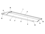
図1乃至図4において、照明装置として天井面へ設置される天井直付けタイプのベースライトが示されており、この照明装置は、横長の略長方形状に形成されている。 FIGS. 1 to 4 show a ceiling-mounted base light installed on a ceiling surface as a lighting device, and this lighting device is formed in a horizontally long, substantially rectangular shape.
照明装置は、装置本体1と、この装置本体1に配設された光源部2と、光源部2を覆う乳白色であって透光性のカバー部材3と、光源部2を点灯制御する点灯装置4と、前記装置本体1の中央部に配設されたセンターカバー5と、側板6とを備えている。このような照明装置は、前面側を光の照射面とし、背面側を天井面への取付面としている。
The lighting device includes a device
図3及び図4に代表して示すように、装置本体1は、横長で略長方形状のシャーシであり、溶融亜鉛めっき鋼板等の熱伝導性を有する金属板を折曲して形成されている。この装置本体1は、放熱部材としての機能を有していて、中央部には、長手方向に沿って平坦な天板面11が形成されており、両側には、長手方向に沿って前面側へ突出する樋状の折曲した配設部12が形成されている。配設部12は、長手方向に沿って細幅の平坦面を有しており、光源部2が配設されるようになっている。
As representatively shown in FIGS. 3 and 4, the apparatus
また、装置本体1の天板面11の両端側には、一対の取付穴11aが形成されている。この取付穴11aには、天井の構造体に設けられた一対の取付ボルトが背面側から貫通し、装置本体1が天井面に設置されるようになっている。
Further, a pair of
なお、装置本体1は、本実施形態においては、シャーシが該当するが、熱伝導性を有し放熱部材としての機能を有していれば、ケース、反射板やベースと指称されるものであってもよく、その部材の名称に拘束されるものではない。一般的には、光源部2が直接的又は間接的に配設される部材や部分を意味しており、格別限定的に解釈されるものではない。
The apparatus
光源部2は、図2乃至図4、図7に代表して示すように、基板21と、この基板21に実装された複数の発光素子22と、各発光素子22を覆う蛍光体層23とを備えている。 なお、図2においては、説明上、一方(図示上、上側)のカバー部材3を透明化して示しており、図7(b)においては、主として基板21の配線パターン層21aを示している。
As representatively shown in FIGS. 2 to 4 and 7, the
基板21は、絶縁材である例えば、ガラスエポキシ樹脂(FR−4)等の材料で細長の長方形状に形成されている。表面側には銅箔で形成された配線パターン層21aが施されている(図7(b)参照)。また、配線パターン層21aの上には、適宜レジスト層21bが施されるようになっている。この基板21は、装置本体1の前面側に後述するカバー部材3を介して複数枚、具体的には、3枚の基板21が長手方向に直線状に並べられて配設されている。したがって、基板21の裏面側は、装置本体1における配設部12の平坦面に面接触して熱的に結合されるようになっている。
The board |
なお、基板21の材料には、セラミックス材料、合成樹脂材料又は各発光素子22の放熱性を高めるうえで、アルミニウム等の熱伝導性が良好で放熱性に優れたべース板の一面に絶縁層が積層された金属製のべース基板を適用することができ、格別その材料が限定されるものではない。
The material of the
配線パターン層21aは、詳しくは、図7(b)に示すように、例えば、略四角形状に形成されて各発光素子22に対応したブロック状のパターンが基板21の長手方向に沿って連続するように並べられて形成されている。全体としては細長の長方形状に形成されていて、これが2列にわたって設けられている。
Specifically, as shown in FIG. 7B, the
この配線パターン層21aは、各発光素子22を電気的に接続する導電層であり、また、各発光素子22から発生する熱を拡散し放熱する放熱層としての機能を併せ持っている。
The
また、基板21の表層には、発光素子22の実装領域や部品の実装部分を除いて、ほとんど全面に反射率の高い白色の前記レジスト層21bが積層されている。これにより発光素子22が放射した光のうちで横方向へ向かった光は、反射率の高い白色のレジスト層21bの表面で反射され前面側へ放射される。
Further, on the surface layer of the
複数の発光素子22は、LEDのベアチップからなる。LEDのベアチップには、例えば、白色系の光を発光部で発光させるために、青色の光を発するものが用いられている。このLEDのベアチップは、シリコーン樹脂系の絶縁性接着剤を用いて配線パターン層21a上に接着され、ボンディングワイヤによって配線パターン層21aに電気的に接続されている。
The plurality of
蛍光体層23は、透光性合成樹脂、例えば、透明シリコーン樹脂製であり、YAG:Ce等の蛍光体を適量含有している。蛍光体層23は、個々の発光素子22を発光素子22ごとに被覆するように高さ寸法の小さい略円筒状をなしている。蛍光体は、発光素子22が発する光で励起されて、発光素子22が発する光の色とは異なる色の光を放射する。発光素子22が青色光を発する本実施形態では、白色光を出射できるようにするために、蛍光体には青色の光とは補色の関係にある黄色系の光を放射する黄色蛍光体が使用されている。
The
なお、蛍光体層23の形状は、個々の発光素子22を被覆できれば、特段限定されるものではなく、山形の形状や複数の発光素子22を連続的に覆うライン状の形態を適用することができる。また、発光素子としては、表面実装型のLEDパッケージを用いるようにしてもよく、実装方式や形式は、格別限定されるものではない。
The shape of the
さらに、本実施形態では、配線パターン層21aは、放熱層として機能するものであるが、配線パターン層21aと放熱層とは、別個に形成するようにしてもよい。この場合、放熱層上に発光素子22が接着されて配置されるが、放熱層は電気的には接続されず、発光素子22の実装パッドとして主として放熱作用を促進する役目を担うこととなる。
Furthermore, in the present embodiment, the
カバー部材3は、図3乃至図5に代表して示すように、アクリル樹脂やポリカーボネート樹脂等の絶縁性の材料から乳白色で透光性を有して押出成形によって作られている。カバー部材3は、長尺のケース状に形成されていて、断面形状が左右対称であり、装置本体1の両側に形成された配設部12に配設されるようになっている。また、このカバー部材3には、前記光源部2が保持される。
As representatively shown in FIGS. 3 to 5, the
より詳しくは、カバー部材3は、前面側が光源部2を長手方向に沿って覆うようになっており、背面側が長手方向に沿って長方形状に開放されて開放部31として構成されている。また、長手方向の両端部は開口32して形成されている。
More specifically, the
さらに、開放部31の長手方向に沿う縁部には、互いに対向して開放する一対の保持溝33が全長に亘って形成されている。この保持溝33は、長手方向に沿う前面側支持部33a及び背面側支持部33bによって形成されている。
また、保持溝33の外側方向には、断面略コ字状であって内側に開放する一対の係止部34が長手方向の全長に亘って形成されている。
Further, a pair of holding
In addition, a pair of locking
このようなカバー部材3には、光源部2が保持溝33に保持されて配設される。具体的には、図3に示すように、基板21をカバー部材3における開口32の一方側から、保持溝44にスライドさせて挿入する。これにより光源部2は、カバー部材3に保持される。このように、カバー部材3に光源部2が保持され、カバー部材3と光源部2とは、一体化される。
In such a
また、図8に示すように、カバー部材3における両端部の開口32には、この開口32を閉塞するパッキン35が取付けられるようになっている。このパッキン35は、シリコーンゴム製であり、透光性を有している。このため、光源部2から入射する光をパッキン35を介して外部に照射することが可能となる。さらに、パッキン35は、後述する側板6に組み合わされてその位置が規制されるようになっている。
Further, as shown in FIG. 8, packings 35 for closing the
次に、主として図3及び図5を参照して光源部2が保持されたカバー部材3の装置本体1への取付状態について説明する。カバー部材3を装置本体1に取付ける際には、まず、断面略コ字状の一対の係止部34のうち、外側の係止部34のコ字状の内面側に、装置本体1の長手方向に沿う端縁部13を挿入して配設する。次いで、内側の係止部34の外面側をストッパ部材36によって係止する。
Next, the attachment state of the
ストッパ部材36は、鍵状に屈曲形成されたストッパ金具であり、係止片部36aとこの係止片部36aと一体的に形成された固定片部36bとから構成されている。また、固定片部36bには、ねじ貫通孔が形成されている。このストッパ部材36の係止片部36aがカバー部材3における係止部34の外面側に係止され、固定片部36bがそのねじ貫通孔を貫通して装置本体1にねじ込まれる取付ねじ36cによって固定される。
The
ストッパ部材36は、カバー部材3の長手方向に沿って複数個、具体的には、3個設けられるようになっており(図3参照)、このストッパ部材36と外側の係止部34の内面側に挿入される装置本体1の端縁部13とによって、カバー部材3の前背方向(図示上、上下方向)の動きが規制されるようになっている。
A plurality of, specifically three,
また、カバー部材3の取付状態においては、光源部2の背面側、すなわち、基板21の背面側がカバー部材3の開放部31を介して装置本体1の平坦な配設部12に面接触して熱的に結合される。換言すれば、カバー部材3は、開放部31を有しているので、前面側へ突出する配設部12がこの開放部31に臨むように配設されるため、配設部12と基板21との熱的結合が可能となる。また、この熱的結合は、カバー部材3の装置本体1への取付けと同時に行われるようになる。
Further, in the attached state of the
加えて、装置本体1における前面側へ突出する配設部12は、その側壁が保持溝33を形成する背面側支持部33bの背面側へ延出する延出壁33cを嵌合支持するようになっている。このため、カバー部材3は、装置本体1の配設部12によって左右方向の動きが規制されるようになっている。
In addition, the
図3及び図6に示すように、点灯装置4は、装置本体1における天板部11の前面側に取付けられている。点灯装置4は、光源部2を点灯制御するものであり、箱状のケース内に回路基板及びこの基板に実装された回路部品を収容して構成されており、商用交流電源ACに接続されていて、この交流電源ACを受けて直流出力を生成する。点灯装置4は、例えば、全波整流回路の出力端子間に平滑コンデンサを接続し、この平滑コンデンサに直流電圧変換回路及び電流検出手段を接続して構成されている。したがって、点灯装置4は、基板21を介して発光素子22に接続されており、その直流出力を発光素子22に供給し、発光素子22を点灯制御するようになっている。
また、天板部11の前面側には、端子台7が取付けられている。この端子台7には、電源線や送り線、調光信号線等の配線部材が接続されるようになっている。
As shown in FIGS. 3 and 6, the
A terminal block 7 is attached to the front side of the
図1乃至図6に示すようにセンターカバー5は、装置本体1の前面側の中央部に配設されている。センターカバー5は、溶融亜鉛めっき鋼板等の金属製の板材から形成されていて、側面形状がV字状をなしている。また、少なくとも表面側には、白色の塗装が施されている。
As shown in FIGS. 1 to 6, the
このセンターカバー5の拡開する長手方向に沿う端縁51(図3参照)には、複数の取付舌片52が形成されている。一方、この取付舌片52と対向する装置本体1側には、切込みによって前面側へ若干膨出変形させて形成した挿入孔14が形成されている。
A plurality of
センターカバー5は、V字状の頂部を中心として、拡開する端縁を幅方向に弾性変形させて、拡開する幅寸法を縮小させることが可能となっている。したがって、センターカバー5を装置本体1に取付ける場合には、センターカバー5を拡開する幅寸法を縮小させるように弾性変形し、取付舌片52を挿入孔14の位置に合わせ、弾性変形を解いて元の状態に復帰させる。これにより、取付舌片52が挿入孔14に挿入され、センターカバー5は装置本体1に取付けられる。
The
センターカバー5が取付けられた状態においては、ストッパ部材36における固定片部36bにセンターカバー5の端縁51が当接されるようになる。したがって、例えば、経時的な振動等によってストッパ部材36の取付ねじ36cに緩みが生じても、ストッパ部材36の外れや過度な動きを抑制できる。これにより、装置本体1と基板21との熱的結合の確実化が期待できる。
加えて、点灯装置4や端子台7、配線部材等は、センターカバー5に覆われ外部からは視認できないようになり、外観性が向上できるようになる。
側板6は、合成樹脂材料から形成され、装置本体1の長手方向の両端部を閉塞するように取付けられている。
When the
In addition, the
The
以上のように構成された照明装置は、カバー部材3に光源部2が保持され、このカバー部材3を放熱部材である装置本体1に取付けることにより、光源部2の背面側、具体的には、基板21の背面側が装置本体1の配設部12に面接触して熱的に結合される。したがって、組立作業性が良好であるとともに、基板21の放熱性を向上でき、発光素子22の温度上昇を抑制することが可能となる。さらに、装置本体1の長手方向に沿う端縁部13は、係止部34のコ字状の内面側に挿入され、係止部34によって覆われるようになるので、端縁部13に特別な加工を施すことなく、端縁部13の鋭利性に起因する危険性を回避することができ、組立作業性の安全性を確保することができる。
In the lighting apparatus configured as described above, the
また、図6に示すように、光源部2が保持されたカバー部材3及び点灯装置4は、装置本体1の前面側に、前背方向(図示上、上下方向)に重ならないように横方向に略同一面に配設されており、また、無駄な内部空間を形成しないように構成されているので照明装置の薄型化の実現が可能となる。
Further, as shown in FIG. 6, the
照明装置の設置状態において、点灯装置4に電力が供給されると、光源部2に直流出力が供給され、基板21を介して発光素子22に通電され、各発光素子22が点灯する。発光素子22から出射された光は、蛍光体層23を透過し、乳白色の透光性のカバー部材3を透過して拡散され、主として下方に放射され所定の配光範囲が照明される。
When power is supplied to the
また、図5に示すようにカバー部材3の係止部34は、装置本体1の端縁部13より外方に延出されるようになっているので、この延出された部位より、発光素子22から横方向に出射される光の一部が外部に放射されるようになる。さらに、発光素子22から長手方向両端部の横方向に出射される光の一部は、透光性のパッキン35から外部に放射されるようになる。これら外部に放射される光は、天井面Cを照射するようになるため、照明の明るさ感を増すことができる。
Further, as shown in FIG. 5, the locking
各発光素子22が点灯することにより熱が発生する。各発光素子22から発生する熱は、配線パターン層21aに伝わり、主として基板21の背面側から装置本体1の配設部12に伝導され、さらに装置本体1の全体に伝導されて放熱される。これによって、発光素子22の温度上昇を抑制することができる。
When each light emitting
この場合、図7(a)、(b)に示すように、カバー部材3における光源部2を保持する手段、すなわち、カバー部材3における保持溝33を形成する前面側支持部33aは、放熱層としての配線パターン層21aが形成された領域外に対応して位置されるようになっている。したがって、配線パターン層21aに伝導された熱が前面側支持部33aに影響するのが緩和され、カバー部材3の熱的変形を抑制することが可能となる。
In this case, as shown in FIGS. 7A and 7B, the means for holding the
以上のように本実施形態によれば、光源部2が保持されたカバー部材3を取付けると同時に、光源部2が装置本体1(放熱部材)と熱的に結合されるので、組立作業性の向上を図ることができるとともに、発光素子22の温度上昇を効果的に抑制することができる照明装置を提供することが可能となる。
As described above, according to the present embodiment, the
なお、本発明は、上記実施形態の構成に限定されることなく、発明の要旨を逸脱しない範囲で種々の変形が可能である。また、上記実施形態は、一例として提示したものであり、発明の範囲を限定することは意図していない。例えば、発光素子は、LEDや有機EL等の固体発光素子が適用できる。 In addition, this invention is not limited to the structure of the said embodiment, A various deformation | transformation is possible in the range which does not deviate from the summary of invention. Moreover, the said embodiment is shown as an example and is not intending limiting the range of invention. For example, the light emitting element can be a solid light emitting element such as an LED or an organic EL.
1・・・装置本体(放熱部材)、2・・・光源部、
3・・・カバー部材、4・・・点灯装置、
5・・・センターカバー、6・・・側板、
21・・・基板、21a・・配線パターン層(放熱層)、
21b・・・レジスト層、22・・・発光素子(LED)、
23・・・蛍光体層、31・・・開放部、
33a・・・前面側支持部(光源部を保持する手段)
DESCRIPTION OF
3 ... cover member, 4 ... lighting device,
5 ... Center cover, 6 ... Side plate,
21... Substrate, 21a .. wiring pattern layer (heat radiation layer),
21b ... resist layer, 22 ... light emitting element (LED),
23 ... phosphor layer, 31 ... open part,
33a ... Front side support section (means for holding light source section)
Claims (3)
この光源部を保持するとともに、光源部の前面側を覆い、背面側を開放する開放部を備え、かつ外面に断面略コ字状であって、内側に開放する係止部が形成された絶縁性を有する透光性のカバー部材と;
このカバー部材における前記断面略コ字状の係止部の外面を係止するストッパ部材を備え、端縁部が前記係止部の内側に挿入された状態で、かつ前記断面略コ字状の係止部の外面が前記ストッパ部材に係止された状態で、前記カバー部材が取付けられているとともに、前記光源部の背面側が前記カバー部材の開放部を介して熱的に結合される熱伝導性を有する放熱部材と;
を具備することを特徴とする照明装置。 A light source unit having a substrate and a light emitting element mounted on the substrate;
Insulation that holds the light source part, covers the front side of the light source part, has an open part that opens the back side, and has a substantially U-shaped cross section on the outer surface, and a locking part that opens inside A translucent cover member having properties;
The cover member includes a stopper member that locks the outer surface of the locking portion having a substantially U-shaped cross section, and an end edge portion is inserted inside the locking portion and has a substantially U-shaped cross section. Heat conduction in which the cover member is attached in a state where the outer surface of the locking portion is locked to the stopper member, and the back side of the light source unit is thermally coupled via the opening portion of the cover member A heat dissipating member having a property;
An illumination device comprising:
前記基板が前記一対の保持溝に挿入された状態で、前記光源部が前記カバー部材に保持されるとともに前記基板が前記配設部に熱的に結合され、かつ前記一対の延出壁が前記配設部に嵌合支持されることを特徴とする請求項1又は請求項2に記載の照明装置。 The heat dissipating member has a disposing portion protruding to the front side, and the cover member includes a pair of holding grooves formed by a front side supporting portion and a back side supporting portion facing the front side supporting portion, A pair of extending walls extending from the back side support part to the back side;
With the substrate inserted into the pair of holding grooves, the light source portion is held by the cover member, the substrate is thermally coupled to the arrangement portion, and the pair of extending walls are The lighting device according to claim 1, wherein the lighting device is fitted and supported by the disposition portion.
Priority Applications (2)
| Application Number | Priority Date | Filing Date | Title |
|---|---|---|---|
| JP2011188355A JP5835560B2 (en) | 2011-08-31 | 2011-08-31 | Lighting device |
| CN2012204396540U CN203052387U (en) | 2011-08-31 | 2012-08-30 | Lighting device |
Applications Claiming Priority (1)
| Application Number | Priority Date | Filing Date | Title |
|---|---|---|---|
| JP2011188355A JP5835560B2 (en) | 2011-08-31 | 2011-08-31 | Lighting device |
Publications (2)
| Publication Number | Publication Date |
|---|---|
| JP2013051118A JP2013051118A (en) | 2013-03-14 |
| JP5835560B2 true JP5835560B2 (en) | 2015-12-24 |
Family
ID=48013009
Family Applications (1)
| Application Number | Title | Priority Date | Filing Date |
|---|---|---|---|
| JP2011188355A Expired - Fee Related JP5835560B2 (en) | 2011-08-31 | 2011-08-31 | Lighting device |
Country Status (1)
| Country | Link |
|---|---|
| JP (1) | JP5835560B2 (en) |
Families Citing this family (3)
| Publication number | Priority date | Publication date | Assignee | Title |
|---|---|---|---|---|
| JP2013077400A (en) * | 2011-09-29 | 2013-04-25 | Toshiba Lighting & Technology Corp | Lighting device |
| JP6747807B2 (en) * | 2014-01-30 | 2020-08-26 | 興和株式会社 | Lighting equipment |
| JP6948599B2 (en) * | 2017-11-22 | 2021-10-13 | 東芝ライテック株式会社 | lighting equipment |
Family Cites Families (1)
| Publication number | Priority date | Publication date | Assignee | Title |
|---|---|---|---|---|
| JP2010123552A (en) * | 2008-11-24 | 2010-06-03 | Toshiba Lighting & Technology Corp | Luminaire |
-
2011
- 2011-08-31 JP JP2011188355A patent/JP5835560B2/en not_active Expired - Fee Related
Also Published As
| Publication number | Publication date |
|---|---|
| JP2013051118A (en) | 2013-03-14 |
Similar Documents
| Publication | Publication Date | Title |
|---|---|---|
| US8567999B2 (en) | Lighting apparatus | |
| JP5391767B2 (en) | Light emitting device and lighting apparatus | |
| US8294356B2 (en) | Light-emitting element lamp and lighting equipment | |
| JP2013062163A (en) | Luminaire | |
| JP2013077400A (en) | Lighting device | |
| JP2012244018A (en) | Light-emitting module and illumination apparatus | |
| JP5126631B2 (en) | Light emitting element lamp and lighting apparatus | |
| JP2016195134A (en) | Light source unit | |
| JP5245806B2 (en) | Light source unit and lighting apparatus | |
| JP5835560B2 (en) | Lighting device | |
| TWI509193B (en) | Luminaire | |
| JP2012160264A (en) | Lighting fixture | |
| JP2012243661A (en) | Lighting fixture | |
| JP2013062107A (en) | Luminaire | |
| JP5772661B2 (en) | lighting equipment | |
| JP6297299B2 (en) | lighting equipment | |
| JP5294044B2 (en) | lighting equipment | |
| JP2009206026A (en) | Light-emitting element lamp and lighting fixture | |
| JP2013179014A (en) | Lighting fixture | |
| JP2012160265A (en) | Lighting fixture | |
| JP2012160266A (en) | Lighting fixture | |
| JP2010055939A (en) | Light source unit and lighting fixture | |
| JP5448011B2 (en) | Light emitting element lamp and lighting apparatus | |
| JP2013152901A (en) | Light-emitting device, and lighting device | |
| KR100998560B1 (en) | Light Emittion Diode module having radiant heat and reflection function |
Legal Events
| Date | Code | Title | Description |
|---|---|---|---|
| A621 | Written request for application examination |
Free format text: JAPANESE INTERMEDIATE CODE: A621 Effective date: 20140626 |
|
| A977 | Report on retrieval |
Free format text: JAPANESE INTERMEDIATE CODE: A971007 Effective date: 20150318 |
|
| A131 | Notification of reasons for refusal |
Free format text: JAPANESE INTERMEDIATE CODE: A131 Effective date: 20150327 |
|
| A521 | Written amendment |
Free format text: JAPANESE INTERMEDIATE CODE: A523 Effective date: 20150514 |
|
| A131 | Notification of reasons for refusal |
Free format text: JAPANESE INTERMEDIATE CODE: A131 Effective date: 20150804 |
|
| A521 | Written amendment |
Free format text: JAPANESE INTERMEDIATE CODE: A523 Effective date: 20150916 |
|
| TRDD | Decision of grant or rejection written | ||
| A01 | Written decision to grant a patent or to grant a registration (utility model) |
Free format text: JAPANESE INTERMEDIATE CODE: A01 Effective date: 20151007 |
|
| A61 | First payment of annual fees (during grant procedure) |
Free format text: JAPANESE INTERMEDIATE CODE: A61 Effective date: 20151020 |
|
| LAPS | Cancellation because of no payment of annual fees |