JP2006237055A - Method of manufacturing semiconductor wafer and method of specularly chamfering semiconductor wafer - Google Patents
Method of manufacturing semiconductor wafer and method of specularly chamfering semiconductor wafer Download PDFInfo
- Publication number
- JP2006237055A JP2006237055A JP2005045360A JP2005045360A JP2006237055A JP 2006237055 A JP2006237055 A JP 2006237055A JP 2005045360 A JP2005045360 A JP 2005045360A JP 2005045360 A JP2005045360 A JP 2005045360A JP 2006237055 A JP2006237055 A JP 2006237055A
- Authority
- JP
- Japan
- Prior art keywords
- polishing
- semiconductor wafer
- wafer
- protective film
- mirror
- Prior art date
- Legal status (The legal status is an assumption and is not a legal conclusion. Google has not performed a legal analysis and makes no representation as to the accuracy of the status listed.)
- Pending
Links
Images


Classifications
-
- H—ELECTRICITY
- H01—ELECTRIC ELEMENTS
- H01L—SEMICONDUCTOR DEVICES NOT COVERED BY CLASS H10
- H01L21/00—Processes or apparatus adapted for the manufacture or treatment of semiconductor or solid state devices or of parts thereof
- H01L21/02—Manufacture or treatment of semiconductor devices or of parts thereof
- H01L21/04—Manufacture or treatment of semiconductor devices or of parts thereof the devices having at least one potential-jump barrier or surface barrier, e.g. PN junction, depletion layer or carrier concentration layer
- H01L21/18—Manufacture or treatment of semiconductor devices or of parts thereof the devices having at least one potential-jump barrier or surface barrier, e.g. PN junction, depletion layer or carrier concentration layer the devices having semiconductor bodies comprising elements of Group IV of the Periodic System or AIIIBV compounds with or without impurities, e.g. doping materials
- H01L21/30—Treatment of semiconductor bodies using processes or apparatus not provided for in groups H01L21/20 - H01L21/26
- H01L21/302—Treatment of semiconductor bodies using processes or apparatus not provided for in groups H01L21/20 - H01L21/26 to change their surface-physical characteristics or shape, e.g. etching, polishing, cutting
- H01L21/304—Mechanical treatment, e.g. grinding, polishing, cutting
-
- H—ELECTRICITY
- H01—ELECTRIC ELEMENTS
- H01L—SEMICONDUCTOR DEVICES NOT COVERED BY CLASS H10
- H01L21/00—Processes or apparatus adapted for the manufacture or treatment of semiconductor or solid state devices or of parts thereof
- H01L21/02—Manufacture or treatment of semiconductor devices or of parts thereof
- H01L21/02002—Preparing wafers
- H01L21/02005—Preparing bulk and homogeneous wafers
- H01L21/02008—Multistep processes
-
- B—PERFORMING OPERATIONS; TRANSPORTING
- B24—GRINDING; POLISHING
- B24B—MACHINES, DEVICES, OR PROCESSES FOR GRINDING OR POLISHING; DRESSING OR CONDITIONING OF ABRADING SURFACES; FEEDING OF GRINDING, POLISHING, OR LAPPING AGENTS
- B24B37/00—Lapping machines or devices; Accessories
- B24B37/04—Lapping machines or devices; Accessories designed for working plane surfaces
- B24B37/07—Lapping machines or devices; Accessories designed for working plane surfaces characterised by the movement of the work or lapping tool
- B24B37/08—Lapping machines or devices; Accessories designed for working plane surfaces characterised by the movement of the work or lapping tool for double side lapping
-
- B—PERFORMING OPERATIONS; TRANSPORTING
- B24—GRINDING; POLISHING
- B24B—MACHINES, DEVICES, OR PROCESSES FOR GRINDING OR POLISHING; DRESSING OR CONDITIONING OF ABRADING SURFACES; FEEDING OF GRINDING, POLISHING, OR LAPPING AGENTS
- B24B9/00—Machines or devices designed for grinding edges or bevels on work or for removing burrs; Accessories therefor
- B24B9/02—Machines or devices designed for grinding edges or bevels on work or for removing burrs; Accessories therefor characterised by a special design with respect to properties of materials specific to articles to be ground
- B24B9/06—Machines or devices designed for grinding edges or bevels on work or for removing burrs; Accessories therefor characterised by a special design with respect to properties of materials specific to articles to be ground of non-metallic inorganic material, e.g. stone, ceramics, porcelain
- B24B9/065—Machines or devices designed for grinding edges or bevels on work or for removing burrs; Accessories therefor characterised by a special design with respect to properties of materials specific to articles to be ground of non-metallic inorganic material, e.g. stone, ceramics, porcelain of thin, brittle parts, e.g. semiconductors, wafers
-
- H—ELECTRICITY
- H01—ELECTRIC ELEMENTS
- H01L—SEMICONDUCTOR DEVICES NOT COVERED BY CLASS H10
- H01L21/00—Processes or apparatus adapted for the manufacture or treatment of semiconductor or solid state devices or of parts thereof
- H01L21/02—Manufacture or treatment of semiconductor devices or of parts thereof
- H01L21/02002—Preparing wafers
- H01L21/02005—Preparing bulk and homogeneous wafers
- H01L21/02008—Multistep processes
- H01L21/0201—Specific process step
- H01L21/02021—Edge treatment, chamfering
Abstract
Description
本発明は、半導体ウェーハの製造方法に関し、両面研磨工程等を経て製造する場合に、ウェーハ外周部でも高い平坦度を達成することができる半導体ウェーハの製造方法および半導体ウェーハの鏡面面取り方法に関する。 The present invention relates to a method for manufacturing a semiconductor wafer, and more particularly to a method for manufacturing a semiconductor wafer and a mirror chamfering method for a semiconductor wafer that can achieve high flatness even at the outer peripheral portion of the wafer when manufacturing through a double-side polishing process.
半導体デバイスの製造に使用する半導体ウェーハは、例えば、チョクラルスキー法により育成されたシリコン単結晶インゴットをスライスしてウェーハ形状に加工した後、面取り(研削)、ラッピング、エッチング、片面研磨、面取り部研磨(鏡面面取り)等の各工程を経て製造される。 Semiconductor wafers used for semiconductor device manufacturing are, for example, slicing silicon single crystal ingots grown by the Czochralski method and processing into wafer shapes, then chamfering (grinding), lapping, etching, single-side polishing, chamfered parts It is manufactured through each process such as polishing (mirror chamfering).
近年、半導体デバイスの高集積化に伴うデザイン・ルールの縮小に伴い、シリコンウェーハに要求される平坦度もますます厳しくなっている。さらに、1枚のウェーハから極力多くのデバイスを得ることが望まれ、シリコンウェーハの大口径化と共に、ウェーハ全面、特に外周端部まで平坦な形状が要求されるようになってきている。ウェーハの外周端部においてデバイスチップが取れない、いわゆるウェーハの外周除外領域の縮小化は、従来の3mmから2mmへと進んでおり、さらには1mmの外周除外領域の要求も出始めている。最近、ウェーハ外周部の平坦度は、ロールオフ量と称されるパラメータで評価されている。 In recent years, the flatness required for silicon wafers has become stricter as the design rules have been reduced due to higher integration of semiconductor devices. Furthermore, it is desired to obtain as many devices as possible from a single wafer, and as the diameter of a silicon wafer increases, a flat shape is demanded on the entire surface of the wafer, particularly the outer peripheral edge. The reduction of the so-called outer periphery exclusion area of the wafer, in which device chips cannot be removed at the outer peripheral edge of the wafer, has progressed from the conventional 3 mm to 2 mm, and there is also a demand for an outer periphery exclusion area of 1 mm. Recently, the flatness of the wafer outer peripheral portion has been evaluated by a parameter called a roll-off amount.
また、近年のシリコンウェーハの需要拡大に伴う製造コスト引き下げ要請に対応するために製造されている、300mmφに代表される大口径シリコンウェーハでは、平坦度品質やナノトポグラフィー品質を得るために、表裏面を同時研磨する両面研磨工程が採用されている。両面研磨では片面方式の研磨に比べ、特にエッジロールオフと呼ばれるウェーハ外周部に対する平坦度の精度が得やすいという特徴を持つ。また基準面を持たない加工方法のため、表裏面に存在する1mm〜20mmのナノトポグラフィーと呼ばれるうねり形状を容易に除去する事が出来る。
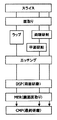
この場合、例えば図12に示されるように、スライス、面取り、ラッピング(両頭研削、平面研削)、エッチング、両面研磨、鏡面面取り、最終研磨の各工程を経て鏡面状のシリコンウェーハを得ることができる。
In addition, in order to obtain flatness quality and nanotopography quality, large-diameter silicon wafers represented by 300 mmφ, which are manufactured to meet the demand for reduction in manufacturing costs accompanying the recent increase in demand for silicon wafers, A double-side polishing process that simultaneously polishes the back surface is employed. Double-side polishing has a feature that flatness accuracy with respect to the outer peripheral portion of the wafer, which is called edge roll-off, can be obtained more easily than single-side polishing. Further, since the processing method does not have a reference surface, a waviness shape called nanotopography of 1 mm to 20 mm existing on the front and back surfaces can be easily removed.
In this case, for example, as shown in FIG. 12, a mirror-like silicon wafer can be obtained through the steps of slicing, chamfering, lapping (double-head grinding, surface grinding), etching, double-side polishing, mirror chamfering, and final polishing. .
然るに、両面研磨工程では、ウェーハキャリアの複数の円形開口部にウェーハを収納してウェーハの両面を同時に研磨するため、研磨中にウェーハの面取り部端面とキャリア内周面が常時接触する。そのため、ウェーハ面取り部端面にキズや圧痕が発生し、これらの欠陥は、キャリア内周面にシリコンより軟質な樹脂を用いてもこれを完全に防ぐ事は困難である。 However, in the double-side polishing step, the wafer is housed in a plurality of circular openings of the wafer carrier and both surfaces of the wafer are polished simultaneously, so that the end surface of the chamfered portion of the wafer and the inner peripheral surface of the wafer are always in contact during polishing. For this reason, scratches and indentations are generated on the end face of the wafer chamfered portion, and it is difficult to completely prevent these defects even if a resin softer than silicon is used on the inner peripheral surface of the carrier.
デバイス製造における成膜処理工程やレジスト樹脂膜塗布工程において、面取り部に酸化膜や窒化膜が形成されたり、レジスト膜が付着する場合があるが、面取り部にキズや圧痕があると、これらの膜成分はその後の洗浄工程等では除去されずに残留して発塵源となり、歩留まりを悪化させる要因となる。しかし、面取り部を鏡面化しておけば、その後付着したレジスト膜等の除去が容易となる。 In the film formation process and the resist resin film coating process in device manufacturing, an oxide film or a nitride film may be formed on the chamfered part, or a resist film may adhere to the chamfered part. The film component remains without being removed in the subsequent cleaning process or the like and becomes a source of dust generation, which becomes a factor of deteriorating the yield. However, if the chamfered portion is mirror-finished, the resist film and the like attached thereafter can be easily removed.
従って、両面研磨の後には、面取り部端面のキズや圧痕を除去するために、面取り部を鏡面研磨する鏡面面取り工程が必須であるが、両面研磨で作り出した優れた外周形状、即ち良好なエッジロールオフ量を、面取り部の鏡面研磨により悪化させる現象が起きている。面取り部の研磨処理は、比較的軟質な研磨パッドが用いられるため、面取り部のみでなく、表面および/または裏面(以下「主面」とも言う)にまで、研磨パッドが入り込む過研磨を避けられず、ロールオフ量の悪化を引き起こす。 Therefore, after double-sided polishing, in order to remove scratches and indentations on the end face of the chamfered part, a mirror chamfering process of mirror-polishing the chamfered part is essential, but an excellent outer peripheral shape created by double-sided polishing, that is, a good edge There is a phenomenon in which the roll-off amount is deteriorated by mirror polishing of the chamfered portion. Since the polishing process of the chamfered portion uses a relatively soft polishing pad, it is possible to avoid overpolishing not only the chamfered portion but also the front surface and / or back surface (hereinafter also referred to as “main surface”). In other words, the roll-off amount is deteriorated.
これに対して、面取り部のキズや裏面の吸着痕を除去する技術として、面取りされたウェーハを、ウェーハ保持板に形成されたウェーハ保持孔に挿入・保持し、この半導体ウェーハに粗い研磨を施す粗研磨工程と、粗研磨後、半導体ウェーハの外周部の面取り面を鏡面仕上げする鏡面面取り工程と、この面取り部の鏡面研磨後、半導体ウェーハの研磨面を仕上げ研磨する仕上げ研磨工程とを備えた半導体ウェーハの製造方法において、面取り部研磨前の粗研磨された半導体ウェーハに酸化膜を形成し、面取り部の鏡面研磨後で仕上げ研磨する前に、上記半導体ウェーハから酸化膜を除去する半導体ウェーハの製造方法が提案されている(特許文献1)。 On the other hand, as a technique for removing scratches on the chamfered portion and suction marks on the back surface, the chamfered wafer is inserted and held in a wafer holding hole formed in the wafer holding plate, and this semiconductor wafer is subjected to rough polishing. A rough polishing step, a mirror chamfering step for mirror finishing the chamfered surface of the outer peripheral portion of the semiconductor wafer after the rough polishing, and a final polishing step for polishing the polishing surface of the semiconductor wafer after mirror polishing of the chamfered portion are provided. In a semiconductor wafer manufacturing method, an oxide film is formed on a roughly polished semiconductor wafer before chamfered portion polishing, and the oxide film is removed from the semiconductor wafer before finish polishing after mirror polishing of the chamfered portion. A manufacturing method has been proposed (Patent Document 1).
本方式では保護膜に酸化膜を使用するため、面取り部のキズや吸着痕を防止できるとともに、特許文献1には明記されていないが、面取り部の鏡面研磨時に主面への過研磨が抑制され、主面の過研磨を防止する効果が得られる可能性がある。但し、この場合酸素雰囲気中での熱処理法による熱酸化膜、CVD法による気相成長膜が必要となるが、その形成には別途酸化炉やCVD炉が必要となり、大幅な設備投資を伴う事になる。更に、面取り部の鏡面研磨後の酸化膜の除去にはふっ酸による洗浄が不可欠であり、特殊な洗浄機の導入も不可欠となる。
Since this method uses an oxide film as the protective film, it can prevent scratches and adsorption marks in the chamfered portion and is not specified in
そこで、本発明は、上記問題点に鑑みてなされたものであって、本発明の目的は、設備投資や工程数の増加等のコスト増を極力排除して半導体ウェーハの面取り部端面部のキズや圧痕を除去し、ウェーハの面取り部を鏡面研磨する鏡面面取り工程において研磨パッドがウェーハの主面に入り込むことによる過研磨を抑制し、ウェーハ外周形状、特にエッジロールオフを悪化させない工程を提供することである。 Accordingly, the present invention has been made in view of the above problems, and an object of the present invention is to eliminate the increase in cost such as capital investment and increase in the number of processes as much as possible, and to scratch the chamfered end face of the semiconductor wafer. In the mirror chamfering process, which removes dents and mirrors the chamfered portion of the wafer, it suppresses overpolishing due to the polishing pad entering the main surface of the wafer, and provides a process that does not deteriorate the wafer outer peripheral shape, especially edge roll-off. That is.
上記目的を達成するために、本発明によれば、少なくとも、半導体ウェーハの表面および裏面を鏡面研磨する両面研磨工程と、該両面研磨された半導体ウェーハの面取り部を鏡面研磨する鏡面面取り工程とを含む半導体ウェーハの製造方法において、前記両面研磨工程の後に、半導体ウェーハの表面または表裏両面に研磨を抑制する樹脂製の保護膜を形成した後、前記鏡面面取り工程を行い、その後に前記樹脂製の保護膜を除去することを特徴とする半導体ウェーハの製造方法が提供される(請求項1)。 In order to achieve the above object, according to the present invention, at least a double-side polishing step for mirror polishing the front and back surfaces of a semiconductor wafer, and a mirror chamfering step for mirror polishing a chamfered portion of the semiconductor wafer polished on both sides. In the manufacturing method of a semiconductor wafer including, after the double-side polishing step, after forming a protective film made of resin that suppresses polishing on the front surface or both sides of the semiconductor wafer, the mirror chamfering step is performed, and then the resin-made chamfering step is performed. A method for producing a semiconductor wafer is provided, wherein the protective film is removed (claim 1).
このように、少なくとも、両面研磨工程と鏡面面取り工程とを含む半導体ウェーハの製造方法において、前記両面研磨工程後に、半導体ウェーハの表面または表裏両面に研磨を抑制する樹脂製の保護膜を形成(塗布)した後、前記鏡面面取り工程を行い、その後に前記樹脂製の保護膜を除去することにより、両面研磨で得られた高精度なウェーハ形状を悪化させることなく、両面研磨工程で劣化した面取り部端面部のキズや圧痕を容易に除去することができ、鏡面面取り工程において研磨パッドが半導体ウェーハの主面に入り込むことによる過研磨を抑制することができ、ウェーハ外周形状、特にエッジロールオフを悪化させる事もない。また、樹脂の塗布工程を追加し、従来の洗浄工程を改良するだけであるので、設備投資や工程数の増加等のコスト増を排除することもできる。 Thus, in the semiconductor wafer manufacturing method including at least a double-side polishing step and a mirror chamfering step, after the double-side polishing step, a resin protective film that suppresses polishing is formed on the front surface or both front and back surfaces of the semiconductor wafer (application) The chamfered portion deteriorated in the double-side polishing step without deteriorating the high-precision wafer shape obtained by double-side polishing by performing the mirror chamfering step and then removing the resin protective film. Scratches and indentations on the end face can be easily removed, over-polishing due to the polishing pad entering the main surface of the semiconductor wafer in the mirror chamfering process can be suppressed, and the wafer outer peripheral shape, especially edge roll-off, is deteriorated. There's nothing to do. Moreover, since only the resin coating process is added and the conventional cleaning process is improved, it is possible to eliminate an increase in cost such as capital investment and an increase in the number of processes.
このとき、前記半導体ウェーハとして、シリコンウェーハを用いることが好ましい(請求項2)。
シリコンウェーハは半導体デバイスの材料として最も需要が高く、特に近年量産されている直径300mm以上に及ぶ大直径のシリコンウェーハの製造では一般的に両面研磨が行われるので、本発明が特に有効となる。
At this time, it is preferable to use a silicon wafer as the semiconductor wafer.
Silicon wafers are most in demand as materials for semiconductor devices, and in particular, double-side polishing is generally performed in the manufacture of large-diameter silicon wafers having a diameter of 300 mm or more, which have been mass-produced in recent years. Therefore, the present invention is particularly effective.
また、前記樹脂製の保護膜として、アルカリ性水溶液に可溶な樹脂を用いることが好ましい(請求項3)。
樹脂製の保護膜として、アルカリ性水溶液に可溶な樹脂を用いることにより、鏡面面取り工程の後に前記樹脂製の保護膜を容易に除去(剥離)することができる。
Further, it is preferable to use a resin soluble in an alkaline aqueous solution as the resin protective film.
By using a resin soluble in an alkaline aqueous solution as the resin protective film, the resin protective film can be easily removed (peeled) after the mirror chamfering step.
さらに、前記樹脂製の保護膜として、半導体ウェーハの研磨レートと同じか遅い特性を持つ樹脂を用いることが好ましい(請求項4)。
鏡面面取り工程において、シリコン面露出部、樹脂製の保護膜による被覆部は同時に接触・研磨されるが、前記樹脂製の保護膜として、半導体ウェーハの研磨レートと同じか遅い特性を持つ樹脂を用いることにより、保護膜被覆部を確実に露出部より研磨されるのを抑制でき、主面の過研磨時の研磨量を抑えることができる。
Furthermore, it is preferable to use a resin having the same or slower characteristics as the polishing rate of the semiconductor wafer as the protective film made of resin.
In the mirror chamfering process, the silicon surface exposed portion and the coating portion with the resin protective film are simultaneously contacted and polished, but the resin protective film is made of a resin having the same or slower characteristics as the polishing rate of the semiconductor wafer. Thus, the protective film covering portion can be reliably prevented from being polished from the exposed portion, and the polishing amount when the main surface is excessively polished can be suppressed.
また、前記樹脂製の保護膜として、アクリル系樹脂を用いることが好ましい(請求項5)。
このように、前記樹脂製の保護膜として、アクリル系樹脂を用いることにより、アルカリ性水溶液に容易に溶解・分解することができ、研磨時の研磨レートをシリコンウェーハより遅くすることができる。
Moreover, it is preferable to use an acrylic resin as the protective film made of resin.
Thus, by using acrylic resin as the protective film made of resin, it can be easily dissolved and decomposed in an alkaline aqueous solution, and the polishing rate at the time of polishing can be made slower than that of the silicon wafer.
さらに、前記樹脂製の保護膜の除去を、アルカリ系洗浄により行うことが好ましい(請求項6)。
このように、前記樹脂製の保護膜の除去を、一般的なアルカリ系の洗浄により容易に行うことができる。また、このような一般的なアルカリ系の洗浄による保護膜の除去においては、特殊な溶剤を使用しないため、地球環境の観点からも優れている。
Furthermore, it is preferable to remove the resin protective film by alkaline cleaning.
In this way, the resin protective film can be easily removed by general alkaline cleaning. Further, in the removal of the protective film by such general alkaline cleaning, since a special solvent is not used, it is excellent from the viewpoint of the global environment.
また、前記樹脂製の保護膜の除去を、苛性ソーダ水溶液と過酸化水素水の混合液による化学洗浄と、アンモニア水と過酸化水素水の混合液による化学洗浄により行うことが好ましい(請求項7)。
一般的な面取り研磨後の洗浄である、アンモニア水と過酸化水素水の混合液による化学洗浄に加え、苛性ソーダ水溶液と過酸化水素水の混合液による化学洗浄を行うことにより、アクリル系樹脂の保護膜を容易に除去することができる。
Further, it is preferable that the protective film made of resin is removed by chemical cleaning with a mixed solution of caustic soda and hydrogen peroxide solution and chemical cleaning with a mixed solution of ammonia water and hydrogen peroxide solution. .
In addition to chemical cleaning with a mixed solution of ammonia water and hydrogen peroxide solution, which is a general cleaning after chamfering polishing, chemical cleaning with a mixed solution of caustic soda solution and hydrogen peroxide solution is performed to protect acrylic resin. The film can be easily removed.
さらに、本発明によれば、少なくとも半導体ウェーハの面取り部を鏡面研磨する半導体ウェーハの鏡面面取り方法において、前記半導体ウェーハの表面または表裏両面に研磨を抑制する樹脂製の保護膜を形成した後、前記鏡面面取り工程を行うことを特徴とする半導体ウェーハの鏡面面取り方法が提供される(請求項8)。 Furthermore, according to the present invention, in the mirror chamfering method of a semiconductor wafer for mirror polishing at least a chamfered portion of the semiconductor wafer, after forming a resin protective film for suppressing polishing on the surface or both front and back surfaces of the semiconductor wafer, A mirror chamfering method for a semiconductor wafer, characterized in that a mirror chamfering step is performed is provided.
このように、半導体ウェーハの鏡面面取り方法において、半導体ウェーハの表面または表裏両面に研磨を抑制する樹脂製の保護膜を形成した後、前記鏡面面取り工程を行うことにより、低コストで面取り部端面部のキズや圧痕を除去することができ、鏡面面取り工程において研磨パッドがウェーハの主面に入り込むことによる過研磨を抑制し、ウェーハ外周形状、特にエッジロールオフを悪化させる事もない。 As described above, in the method of mirror chamfering a semiconductor wafer, after forming a protective film made of resin that suppresses polishing on the front surface or both surfaces of the semiconductor wafer, the mirror chamfering step is performed, so that the chamfered portion end surface portion is obtained at low cost. Scratches and indentations can be removed, overpolishing due to the polishing pad entering the main surface of the wafer in the mirror chamfering process is suppressed, and the wafer outer peripheral shape, particularly edge roll-off, is not deteriorated.
また、前記鏡面面取り工程の後に、前記樹脂製の保護膜を洗浄により除去することが好ましい(請求項9)
このように、前記鏡面面取り工程の後に、前記樹脂製の保護膜を洗浄により除去することにより、容易かつ低コストで半導体ウェーハを製造できる。
Further, it is preferable that the resin protective film is removed by washing after the mirror chamfering step.
As described above, after the mirror chamfering step, the semiconductor protective film can be easily and inexpensively manufactured by removing the resin protective film by washing.
また、前記鏡面面取りする半導体ウェーハとして、表面および裏面を鏡面に両面研磨した半導体ウェーハを用い、該半導体ウェーハに前記樹脂製の保護膜を形成して鏡面面取りすることが好ましい(請求項10)。
これにより、両面研磨後の面取り部端面部のキズや圧痕を低コストで除去することができ、鏡面面取り工程において研磨パッドがウェーハの主面に入り込むことによる過研磨を抑制することができ、両面研磨で得られた高精度のウエーハ外周形状を維持できる。
Further, as the semiconductor wafer to be mirror chamfered, it is preferable to use a semiconductor wafer having a front surface and a back surface polished to a mirror surface, and to form the resin protective film on the semiconductor wafer to be mirror chamfered (claim 10).
As a result, scratches and indentations on the end surface of the chamfered portion after double-side polishing can be removed at low cost, and overpolishing due to the polishing pad entering the main surface of the wafer in the mirror chamfering step can be suppressed. A highly accurate wafer outer peripheral shape obtained by polishing can be maintained.
このように、本発明により、設備投資や工程数の増加等のコスト増を極力排除して、面取り部端面部のキズや圧痕を除去することができ、鏡面面取り工程において研磨パッドがウェーハの主面に入り込むことによる過研磨を抑制し、ウェーハ外周形状、特にエッジロールオフを悪化させない工程を構築することができる。
特に、樹脂の塗布工程を追加し、従来の洗浄工程を改良するだけで、大幅な工程変更や設備投資を伴う事もなく、今後増加するであろう厳しい顧客のウェーハ外周部に対する平坦度(ロールオフ量)の要求を満足することが可能となった。
As described above, according to the present invention, it is possible to eliminate the increase in cost such as capital investment and the number of processes as much as possible, and to remove the scratches and indentations on the end surface of the chamfered portion. Overpolishing due to entering the surface can be suppressed, and a process that does not deteriorate the wafer outer peripheral shape, particularly edge roll-off, can be constructed.
In particular, by adding a resin coating process and improving the conventional cleaning process, there will be no significant process change or capital investment, and the flatness (roll) of the strict customer's wafer outer periphery will increase in the future. It was possible to satisfy the demand for (off amount).
以下、添付の図面に基づいて本発明について具体的に説明するが、本発明はこれらに限定されるものではない。
近年の半導体デバイスの高集積化、需要増大に伴って、シリコンウェーハの大口径化と共に、ウェーハ全面、特に外周部まで平坦な形状のシリコンウェーハが要求されるようになり、本発明者らは、この要求に応えるべく研究を重ねた。
本研究の中で、本発明者らはシリコンウェーハの両面研磨を行った後、面取り部の研磨を行った場合のウェーハの外周形状について調査を行った。
Hereinafter, the present invention will be specifically described with reference to the accompanying drawings, but the present invention is not limited thereto.
With the recent increase in integration and demand of semiconductor devices, the silicon wafer has become larger, and a silicon wafer having a flat shape up to the entire wafer surface, particularly the outer periphery, has been required. Research was repeated to meet this demand.
In this study, the inventors investigated the outer peripheral shape of the wafer when the chamfered portion was polished after performing double-side polishing of the silicon wafer.
ウェーハの平坦度を評価する場合、従来行われているSFQRやSBIRで定義されるサイトフラットネスでは、図14に示されるような所定の大きさのセル100に分けて評価を行うため、面取り部付近の外周形状を正確に把握することができない。
そこで、最近ではウェーハの外周形状を高精度に評価するため、ロールオフと呼ばれる評価基準が採用されつつある。ロールオフというパラメータは、ウェーハの外周部の形状を直接測定し、高精度に評価することができる。なお、ロールオフの定義については標準化団体で標準化が検討されているが、例えば図16に示されるように、ウェーハ表面に対し、プリズム90を介してレーザ光を照射し、反射光をCCD91で受けることにより測定する方法がある。そして表面プロファイルから基準線を算出し、基準線との差としてロールオフ量を求めることができる。
In the case of evaluating the flatness of a wafer, in the conventional site flatness defined by SFQR or SBIR, the evaluation is divided into
Therefore, recently, an evaluation criterion called roll-off is being adopted in order to accurately evaluate the outer peripheral shape of the wafer. The roll-off parameter can be evaluated with high accuracy by directly measuring the shape of the outer periphery of the wafer. As for the definition of roll-off, standardization is being studied by a standardization organization. For example, as shown in FIG. 16, the wafer surface is irradiated with laser light via a
本発明者らは、シリコンウェーハを両面研磨し、さらに面取り部の研磨を行った後のロールオフ量を測定したところ、図15に示すような結果が得られた。ここで面取り部Cの幅は0.3mm程度以下であるが、主面の面取り部付近でのロールオフ量が大きいことが分かった。
さらに、面取り部研磨後の面取り部と主面との境界付近を顕微鏡で観察したところ、図13に見られるように面取り部との境を越えたウェーハ面内での過研磨領域が観察された。
これらの調査結果から、面取り部の研磨の際、過研磨に起因したフラットネス(ロールオフ)の悪化が極めて大きいことが分かった。
The inventors measured the roll-off amount after double-side polishing the silicon wafer and further polishing the chamfered portion, and the results shown in FIG. 15 were obtained. Here, the width of the chamfered portion C is about 0.3 mm or less, but it has been found that the roll-off amount in the vicinity of the chamfered portion of the main surface is large.
Furthermore, when the vicinity of the boundary between the chamfered portion and the main surface after polishing the chamfered portion was observed with a microscope, an overpolished region in the wafer surface beyond the boundary with the chamfered portion was observed as seen in FIG. .
From these investigation results, it was found that the flatness (roll-off) was greatly deteriorated due to overpolishing when the chamfered portion was polished.
そこで本発明者らは、上記のような過研磨を効果的に防ぐ方法について鋭意研究を行い、本発明を完成させた。
すなわち、本発明者らは、少なくとも、半導体ウェーハの表面および裏面を鏡面研磨する両面研磨工程と、該両面研磨された半導体ウェーハの面取り部を鏡面研磨する鏡面面取り工程とを含む半導体ウェーハの製造方法において、前記両面研磨工程の後に、半導体ウェーハの表面または表裏両面に研磨を抑制する樹脂製の保護膜を形成した後、前記鏡面面取り工程を行い、その後に前記樹脂製の保護膜を除去することにより、設備投資や工程数の増加等のコスト増を極力排除して両面研磨後の面取り部端面部のキズや圧痕を除去することができ、鏡面面取り工程において研磨パッドがウェーハの主面に入り込むことによる過研磨を抑制でき、ウェーハ外周形状、特にエッジロールオフを悪化させる事もないことを見出した。
Therefore, the present inventors have conducted intensive research on a method for effectively preventing the above-described overpolishing and completed the present invention.
That is, the present inventors at least include a double-side polishing step for mirror-polishing the front and back surfaces of a semiconductor wafer, and a mirror-chamfering step for mirror-polishing a chamfered portion of the double-side polished semiconductor wafer. Then, after the double-side polishing step, after forming a resin protective film that suppresses polishing on the front surface or both sides of the semiconductor wafer, the mirror chamfering step is performed, and then the resin protective film is removed. Eliminates scratches and indentations on the end face of the chamfered part after double-side polishing, eliminating cost increases such as capital investment and an increase in the number of processes, and the polishing pad enters the main surface of the wafer in the mirror chamfering process. It has been found that overpolishing due to this can be suppressed and that the wafer outer peripheral shape, particularly edge roll-off, is not deteriorated.
先ず、図2の概略図により本発明について説明する。図2(A)は、本発明にかかる樹脂製の保護膜によるコーティング方式による、シリコンウェーハの鏡面面取り工程の一例を示す概略断面図と、その後樹脂製の保護膜を除去したウェーハの概略断面図であり、図2(B)は、従来方式によるシリコンウェーハの鏡面面取り工程の一例を示す概略断面図と、鏡面面取り工程前後のウェーハの概略断面図である。本発明に係るコーティング方式では、両面研磨工程の後に、半導体ウェーハの表面または表裏両面に研磨を抑制する樹脂製の保護膜2を形成した後、鏡面面取り工程を行い、その後に前記樹脂製の保護膜2を除去する。これにより、従来方式では、研磨前の形状4から研磨後の形状5Bまで過研磨されるのに対して、本発明に係るコーティング方式では、主面が保護膜2で保護されているので、研磨前の形状4から研磨後の形状5Aまでしか研磨されず、鏡面面取り工程において研磨パッドがウェーハの主面に入り込むことによる過研磨を抑えることができる。
First, the present invention will be described with reference to the schematic diagram of FIG. FIG. 2A is a schematic cross-sectional view showing an example of a mirror chamfering process of a silicon wafer by a coating method using a resin protective film according to the present invention, and a schematic cross-sectional view of a wafer after removing the resin protective film. FIG. 2B is a schematic sectional view showing an example of a mirror chamfering process of a silicon wafer according to a conventional method, and a schematic sectional view of the wafer before and after the mirror chamfering process. In the coating method according to the present invention, after the double-side polishing step, the resin
具体的には、例えば、ウェーハ端面からの所定の距離Xにおいて、本発明に係るコーティング方式と従来方式とを比較した場合、従来方式では矢印で示されたロールオフ量6が大きいのに対し、本発明に係るコーティング方式では小さく或いは図2(A)のようにほとんどゼロに抑制することができる。
Specifically, for example, when the coating method according to the present invention is compared with the conventional method at a predetermined distance X from the wafer end surface, the roll-
以下、本発明の実施形態について、図面に基づいて時系列的に説明する。
まず、チョクラルスキー法(CZ法)、浮遊帯域溶融法(FZ法)等により育成したシリコン単結晶インゴットをワイヤソー等を用いてスライスしてウェーハ状とする(図1(A))。
Hereinafter, embodiments of the present invention will be described in time series based on the drawings.
First, a silicon single crystal ingot grown by Czochralski method (CZ method), floating zone melting method (FZ method) or the like is sliced using a wire saw or the like to form a wafer (FIG. 1A).
次いで、ウェーハの外縁部のワレやカケを防止するため、ウェーハの外縁の角部を研削により除去する面取り加工を行う(図1(B))。
面取り加工は、例えば図3に示すように、所望のウェーハ面取り形状と同じ形状を有する砥石1aの溝2aにウェーハ外周端部を押しつけ、保持盤3aに保持されたウェーハWの上面側と下面側の角と最外周部(端面)を一度に面取りして面取り部Cを形成することができる。
Next, in order to prevent cracking or chipping of the outer edge portion of the wafer, chamfering is performed to remove the corner portion of the outer edge of the wafer by grinding (FIG. 1B).
For example, as shown in FIG. 3, the chamfering process is performed by pressing the outer peripheral edge of the wafer against the
また、図3(B)に示すように、ウェーハWと砥石の相対位置を数値制御し、逆台形形状の溝2bを有する砥石1bを用いて、溝2bの底面で、保持盤3bに保持されたウェーハの最外周部(端面)を研削し、溝2bの上側のテーパ面でウェーハWの上面側の角を、溝2bの下側のテーパ面でウェーハWの下面側の角を面取り加工することもできる。
Further, as shown in FIG. 3B, the relative position between the wafer W and the grindstone is numerically controlled, and the
面取り加工後、ウェーハの厚さを均一にするとともに平坦度を高めるため、ラッピングを行う(図1(C))。
なお、面取り加工の前にラッピングを行っても良い。また、ラッピングの代わりに、一対の研削砥石を用いてウェーハの両面を同時に研削する両頭研削、あるいは保持盤に固定したウェーハに対し、砥石により片面ずつ研削を行う平面研削を行うこともできる。両頭研削と平面研削の両方を行っても良い。
After the chamfering process, lapping is performed in order to make the wafer thickness uniform and increase the flatness (FIG. 1C).
Note that lapping may be performed before chamfering. Further, instead of lapping, double-headed grinding in which both surfaces of a wafer are ground simultaneously using a pair of grinding wheels, or surface grinding in which a wafer fixed to a holding plate is ground on each side with a grinding stone can be performed. Both double-head grinding and surface grinding may be performed.
ラッピング等によりウェーハの表面に生じた加工歪みを除去するため、ウェーハをエッチング液に浸漬してエッチングを行う(図1(D))。
例えば水酸化ナトリウムや水酸化カリウムの水溶液を用いたアルカリエッチング、あるいはフッ酸と硝酸の混合液等を用いた酸エッチングを行うことができる。
In order to remove processing distortion generated on the surface of the wafer by lapping or the like, the wafer is immersed in an etching solution for etching (FIG. 1D).
For example, alkali etching using an aqueous solution of sodium hydroxide or potassium hydroxide, or acid etching using a mixed solution of hydrofluoric acid and nitric acid can be performed.
次いで、半導体ウェーハの表面および裏面を鏡面研磨する両面研磨工程を行う(図1(E))。両面研磨工程は、例えば図4に示すような装置70を用いて行われる。この装置70では、図5に示されるようなキャリア75の円形孔78内にウェーハWを収容し、研磨パッド73,74を貼り付けた上下一対の定盤71,72の間に挟み込み、研磨スラリーを供給するとともに、インターナルギア76とサンギア77とにより、上下の定盤71,72とキャリア75を回転させることでウェーハWの両面を同時に研磨する。キャリア75を回転させることでウェーハWの両面を同時に研磨することができる。
Next, a double-side polishing process is performed in which the front and back surfaces of the semiconductor wafer are mirror-polished (FIG. 1E). The double-side polishing step is performed using, for example, an
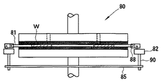
また、例えば図6及び図7に示されるような両面研磨装置80を用いることもできる。この装置80では、研磨の際、全ての偏心アーム82をタイミングチェーン85を介して回転軸90を中心に同期して回転させることにより、キャリアホルダ88に保持されたキャリア81が、自転せずに水平面内で小さな円を描くようにして円運動を行う。このような揺動式の両面研磨装置80であれば小型化することができるため、比較的狭いスペースで大直径ウェーハの研磨作業を行うことができる。近年のウェーハの大直径化に伴い、このような揺動式の両面研磨装置80も多く用いられている。
Further, for example, a double-
このような両面研磨を行うことにより、ウェーハWの表面粗さが改善され、平坦度を向上することができるが、このようにして両面研磨を行う場合、ウェーハWの外縁部(面取り部C)と、キャリア75あるいは81の円形孔78あるいは84の内側面が接触し、ウェーハWの面取り部Cにキズや圧痕が発生することになる。
これらのキズ等を除去するため、該両面研磨されたウェーハWの面取り部Cを鏡面研磨する鏡面面取り工程を行うが、本発明において、この鏡面面取り工程の前に、半導体ウェーハの表面または表裏両面に研磨を抑制する樹脂製の保護膜を形成(塗布)する(図1(F))。
By performing such double-side polishing, the surface roughness of the wafer W can be improved and the flatness can be improved, but when performing double-side polishing in this way, the outer edge portion (chamfered portion C) of the wafer W. Then, the inner surface of the
In order to remove these scratches and the like, a mirror chamfering process is performed in which the chamfered portion C of the wafer W polished on both sides is mirror-polished. In the present invention, before the mirror chamfering process, the surface or both front and back surfaces of the semiconductor wafer are processed. A resin protective film that suppresses polishing is formed (applied) (FIG. 1F).
研磨を抑制する樹脂製の保護膜として、アルカリ性水溶液に可溶でかつ、シリコンウェーハの研磨レートより遅い特性を持つ樹脂として、アクリル系樹脂を用いる。アクリル系樹脂を用いることにより、アルカリ性水溶液に容易に溶解・分解することができるし、研磨時の研磨レートをシリコンウェーハより遅くすることができるからである。 An acrylic resin is used as a resin protective film that suppresses polishing, as a resin that is soluble in an alkaline aqueous solution and has characteristics that are slower than the polishing rate of a silicon wafer. By using an acrylic resin, it can be easily dissolved and decomposed in an alkaline aqueous solution, and the polishing rate at the time of polishing can be made slower than that of a silicon wafer.
研磨を抑制する樹脂製の保護膜として、アクリル系樹脂に限定されないが、アルカリ水溶液に可溶でかつ、シリコンウェーハの研磨レートと同じか遅い特性を持つ樹脂を用いることが好ましい。樹脂製の保護膜としてアルカリ性水溶液に可溶な樹脂を用いることにより、鏡面面取り工程の後における樹脂製の保護膜の除去が容易となり、また、樹脂製の保護膜としてシリコンウェーハの研磨レートと同じか遅い特性を持つ樹脂を用いることにより、次の鏡面面取り工程において、シリコン面露出部、樹脂製の保護膜による被覆部が同時に接触・研磨される際に、保護膜の被覆部は露出部面より研磨されにくいため、主面への過研磨を抑えることができる。 The resin protective film that suppresses polishing is not limited to an acrylic resin, but it is preferable to use a resin that is soluble in an alkaline aqueous solution and has characteristics that are the same as or slower than the polishing rate of a silicon wafer. By using a resin soluble in an alkaline aqueous solution as the resin protective film, it becomes easy to remove the resin protective film after the mirror chamfering process, and the same as the polishing rate of the silicon wafer as the resin protective film By using a resin with slow properties, when the silicon surface exposed part and the resin protective film coated part are simultaneously contacted and polished in the next mirror chamfering process, the protective film coated part becomes the exposed part surface. Since it is harder to polish, overpolishing to the main surface can be suppressed.
ウエーハ上に保護膜を形成するには、例えばアクリル系樹脂をアルコールを溶剤とし流動性とさせ、スピンコーターにより表面に塗布する。この際、スピン回転は高く設定し、面取り部端面部には樹脂が塗布されないようにし、ベーク・乾燥後、次の鏡面面取り工程を行う。保護膜の形成方法は、スピンコーターに限られず、ハケによる塗布等一般に用いられている方法により行うことができる。 In order to form a protective film on the wafer, for example, an acrylic resin is made fluid with alcohol as a solvent and applied to the surface by a spin coater. At this time, the spin rotation is set high so that the resin is not applied to the end surface portion of the chamfered portion, and the next mirror chamfering step is performed after baking and drying. The method for forming the protective film is not limited to the spin coater, and can be performed by a generally used method such as coating by brush.
保護膜の形成は、ロールオフが特に問題となる表面のみに行っても従来にくらべ改善効果が得られるが、表裏両面に行った方がより外周形状の改善を図ることができる。両面に保護膜を形成する場合は、例えば、片面に保護膜をコートし、ベーク後、ウェーハを裏返えして、裏面に保護膜をコートし、ベーク後、鏡面面取り工程を行えばよい。 Even if the protective film is formed only on the surface where the roll-off is particularly problematic, an improvement effect can be obtained as compared with the conventional case, but the outer peripheral shape can be improved more when the protective film is formed on both surfaces. When forming protective films on both sides, for example, a protective film may be coated on one side, after baking, the wafer is turned over, a protective film is coated on the back side, and a mirror chamfering process may be performed after baking.
次に、該両面研磨され保護膜が形成されたウェーハWの面取り部Cを鏡面研磨する鏡面面取り工程を行う(図1(G))。
上記のようにアクリル系樹脂の保護膜が、表面に塗布され、面取り部端面部には塗布されないようにしたウェーハWを、鏡面研磨する。この鏡面面取り工程により、面取り部端面部が優先的に磨かれ、主面内への研磨の回り込みが抑えられる。
面取り部Cの鏡面研磨には、一般に提案されている各種の研磨方法、研磨装置を利用する。例えば、図8に示されるように、吸着盤13でウェーハWを保持し、外周に研磨パッド12を貼付した回転ドラム11に対し、研磨面12aに対し傾斜させたウェーハWの面取り部を一定圧力で押し付けて、コロイダルシリカ等を含有する研磨スラリーを供給しながら、面取り部を研磨する方法がある。
Next, a mirror chamfering process is performed to mirror polish the chamfered portion C of the wafer W on which the protective film is formed by double-side polishing (FIG. 1G).
As described above, the protective film of the acrylic resin is applied to the surface, and the wafer W that is not applied to the end surface portion of the chamfered portion is mirror-polished. By this mirror chamfering process, the end surface portion of the chamfered portion is polished preferentially, and the wraparound of polishing into the main surface is suppressed.
For mirror polishing of the chamfered portion C, various generally proposed polishing methods and polishing apparatuses are used. For example, as shown in FIG. 8, the chamfered portion of the wafer W that is inclined with respect to the polishing
また、図9に示されるように、吸着盤13上で保持されて回転するウェーハWの面取り部に対し、傾斜した研磨面21a,22aを有する研磨パッド21,22と、垂直な面を有する研磨パッド24をそれぞれ押し付けて面取り部全体を研磨する方法や、図10(A)(B)に示されるように、逆カップ型の研磨パッド31をウェーハWの面取り部に押し付けて、面取り部の主面側の面取り面を研磨し、次いで、端面(最外周面)に垂直な研磨パッド34を押し付けて面取り部の端面の研磨を行う方法がある。
Further, as shown in FIG. 9, polishing
このような鏡面面取り工程の後、樹脂製の保護膜の除去(図1(H))を、アルカリ系の洗浄により行う。
一般的なアルカリ系の洗浄により容易に、樹脂製の保護膜の除去を行うことができ、また、特殊な溶剤を使用しないため、地球環境の観点からも優れている。特に、保護膜の除去を、苛性ソーダ水溶液と過酸化水素水の混合液による化学洗浄と、アンモニア水と過酸化水素水の混合液による化学洗浄により行うことが好ましく、苛性ソーダ水溶液と過酸化水素水の混合液による化学洗浄により、アクリル系樹脂の保護膜を除去することができ、その後、アンモニア水と過酸化水素水の混合液による化学洗浄をすることにより、一般的な面取り研磨後の洗浄を行うことができる。すなわち、保護膜の除去は、一般に行われている洗浄工程に対し苛性ソーダ水溶液と過酸化水素水の混合液による化学洗浄を付加するだけでよい。
After such a mirror chamfering step, the resin protective film is removed (FIG. 1H) by alkaline cleaning.
The protective film made of resin can be easily removed by general alkaline cleaning, and since a special solvent is not used, it is excellent from the viewpoint of the global environment. In particular, it is preferable to remove the protective film by chemical cleaning with a mixed solution of caustic soda aqueous solution and hydrogen peroxide solution, and chemical cleaning with a mixed solution of ammonia water and hydrogen peroxide solution. The protective film of the acrylic resin can be removed by chemical cleaning with a mixed solution, and then cleaning after general chamfering polishing is performed by chemical cleaning with a mixed solution of ammonia water and hydrogen peroxide solution. be able to. That is, the removal of the protective film only requires chemical cleaning with a mixed solution of an aqueous caustic soda solution and a hydrogen peroxide solution to a generally performed cleaning process.
さらに、樹脂製の保護膜の除去を行った後、最終研磨を行う(図1(I))。このような最終研磨は、例えばウェーハの片面を吸着保持し、研磨スラリーを供給しながらデバイスを形成する側のみを片面研磨することができる。ウェーハをワックス等の接着剤を介してプレートに貼り付けて片面研磨を行っても良い。なお、この最終研磨で研磨代が多くなると、ウェーハの外周領域の平坦度の悪化を招くおそれがあるので、研磨代は2μm以下、特に1μm程度とするのが好ましい。 Further, after removing the protective film made of resin, final polishing is performed (FIG. 1I). In such final polishing, for example, one side of the wafer can be adsorbed and held, and only the side on which the device is formed can be polished on one side while supplying the polishing slurry. One-side polishing may be performed by attaching the wafer to a plate via an adhesive such as wax. If the polishing allowance increases in this final polishing, the flatness of the outer peripheral region of the wafer may be deteriorated. Therefore, the polishing allowance is preferably 2 μm or less, particularly about 1 μm.
以上のような工程を経てシリコンウェーハを製造すれば、設備投資や工程数の増加等のコスト増を極力排除して、両面研磨工程で生じた面取り部端面部のキズ等を除去することが可能であり、また、面取り部付近の主面の過研磨は防止され、ウェーハ外周形状、特にエッジロールオフを悪化させることもないため、面取り部付近においても、両面研磨により作り込まれたフラットネスが維持された高平坦度の鏡面シリコンウェーハを製造することができ、ウェーハ1枚から得られるデバイスチップの生産性および歩留まりの向上等に貢献できる。 If a silicon wafer is manufactured through the above-mentioned processes, it is possible to eliminate the cost increase such as capital investment and increase in the number of processes as much as possible, and to remove scratches and the like on the end face of the chamfered part generated in the double-side polishing process. In addition, over-polishing of the main surface near the chamfered portion is prevented, and the wafer outer peripheral shape, particularly edge roll-off, is not deteriorated. A mirror silicon wafer having a high flatness that is maintained can be manufactured, which can contribute to an improvement in the productivity and yield of device chips obtained from one wafer.
以下、実施例及び比較例を示して本発明をより具体的に説明するが、本発明はこれらに限定されるものではない。
(実施例)
スライス、面取り、ラッピング、エッチングの各処理を順次行って得た直径300mmのシリコンウェーハに対し、図6に示したような両面研磨装置を用いて両面研磨を行った。
両面研磨後、アクリル製の樹脂(商品名:日化精工社製スカイコート)をスピンコーターで塗布することによりウェーハWの両面に保護膜を約3μmの厚さで形成した。この時、スピンコーターの回転数を1200rpmとし、保護膜が表裏の主面にのみ形成されるようにし、ウェーハ端面に保護膜が形成されないようにした。その後、研磨パッドに対してウェーハWの面取り部における各主面側の面取り面を接触させて面取り部の鏡面研磨を行った(図2(A):図では便宜上、保護膜は片面のみ示されている)。
EXAMPLES Hereinafter, although an Example and a comparative example are shown and this invention is demonstrated more concretely, this invention is not limited to these.
(Example)
Double-side polishing was performed using a double-side polishing apparatus as shown in FIG. 6 on a silicon wafer having a diameter of 300 mm obtained by sequentially performing the respective processes of slicing, chamfering, lapping and etching.
After double-side polishing, an acrylic resin (trade name: Nichika Seiko Co., Ltd. Skycoat) was applied with a spin coater to form a protective film on both sides of the wafer W with a thickness of about 3 μm. At this time, the rotation speed of the spin coater was set to 1200 rpm, the protective film was formed only on the front and back main surfaces, and the protective film was not formed on the wafer end surface. Thereafter, the chamfered surface of each chamfered portion of the chamfered portion of the wafer W was brought into contact with the polishing pad to perform mirror polishing of the chamfered portion (FIG. 2A). ing).
この鏡面面取り工程では、スピードファム社製IV型鏡面面取り機を使用し、図8(A)に示すように研磨パッドの研磨面に対してウェーハWを吸着盤13で保持し、外周に研磨パッド12を貼付した回転ドラム11に対し、傾斜させたウェーハWの面取り部を一定圧力で押し付けて面取り部を鏡面研磨した。研磨パッドとしては、ロデール社製SUBA400を使用し、研磨剤として日産化学社製のAJ1325をベースとしてpH11.0に調整した研磨スラリーを2リットル/分の流量で供給し、研磨荷重を2.0kgfとして面取り部の研磨を行った。
In this mirror chamfering process, an IV type mirror chamfering machine manufactured by Speed Fam Co., Ltd. is used, and the wafer W is held on the polishing surface of the polishing pad by the
その後、アクリル製樹脂の保護膜の除去を、苛性ソーダ水溶液と過酸化水素水の混合液((容量比)48%苛性ソーダ水溶液:20%過酸化水素水:純水=1:1:10)による化学洗浄と、アンモニア水と過酸化水素水の混合液((容量比)30%アンモニア水:20%過酸化水素水:純水=1:1:10)による化学洗浄により行った後、片面研磨装置を用い、ウェーハWの片面に対して最終研磨を施した。この最終研磨では、面取り部研磨工程で用いたスラリーと同じものを供給し、研磨代が1μm程度となるように行った。 Thereafter, the protective film of the acrylic resin is removed by chemistry with a mixture of caustic soda aqueous solution and hydrogen peroxide solution ((volume ratio) 48% caustic soda aqueous solution: 20% hydrogen peroxide solution: pure water = 1: 1: 10). After performing cleaning and chemical cleaning with a mixed solution of ammonia water and hydrogen peroxide water ((volume ratio) 30% ammonia water: 20% hydrogen peroxide water: pure water = 1: 1: 10), a single-side polishing apparatus Was used to perform final polishing on one side of the wafer W. In this final polishing, the same slurry as that used in the chamfered portion polishing step was supplied so that the polishing allowance was about 1 μm.
最終研磨後において、ロールオフ量の測定を行った。ロールオフ測定には、図16に示したようなロールオフ測定機(コベルコ科研社製、LER−310M)を使用した。測定条件は、ウェーハ端面から3mmから6mmの領域を最小自乗法により算出した基準外挿線を基準に、ウェーハ端面から1mmの位置のロールオフ量を計測した。
After the final polishing, the roll-off amount was measured. For the roll-off measurement, a roll-off measuring machine (manufactured by Kobelco Kaken Co., Ltd., LER-310M) as shown in FIG. 16 was used. As the measurement conditions, the roll-off amount at a
(比較例)
実施例と同様にして、スライス、面取り、ラップ、エッチング、両面研磨の各処理を順次行って得たウェーハWに対し、保護膜を形成することなく面取り部研磨を行った。面取り部研磨は、図8(A)に示すような回転ドラムの周囲に研磨パッドを貼り付けた鏡面面取り機(スピードファム社製IV型)を用いて行った。面取り部研磨後、さらに実施例と同様に、ウェーハWの片面に対して最終研磨を施した。
最終研磨後において、ウェーハWのロールオフをそれぞれ測定した。
(Comparative example)
In the same manner as in the example, the chamfered portion was polished without forming a protective film on the wafer W obtained by sequentially performing the respective processes of slicing, chamfering, lapping, etching, and double-side polishing. The chamfered portion polishing was performed using a mirror chamfering machine (IV type manufactured by Speedfam Co., Ltd.) in which a polishing pad was attached around a rotating drum as shown in FIG. After the chamfered portion was polished, final polishing was performed on one side of the wafer W as in the example.
After the final polishing, the roll-off of the wafer W was measured.
実施例及び比較例で測定したロールオフ量の結果をそれぞれ表1および図11に、本発明のコーティング方式、従来方式として示した。 The results of roll-off amounts measured in Examples and Comparative Examples are shown in Table 1 and FIG. 11 as the coating method of the present invention and the conventional method, respectively.

最終研磨後において、比較例の従来方式では、ロールオフ量(平均値)は、0.22×10⁻²mmであり大きかった。一方、実施例のコーティング方式では、0.01×10⁻²mmとほぼゼロになった。このように、本発明は、ウェーハ外周形状、特にエッジロールオフを悪化させることのない優れたものであることが明らかになった。 After the final polishing, in the conventional method of the comparative example, the roll-off amount (average value) was as large as 0.22 × 10 −2 mm. On the other hand, in the coating system of the Example, it became almost zero with 0.01 * 10 <-2> mm. As described above, it was revealed that the present invention is excellent without deteriorating the wafer outer peripheral shape, particularly the edge roll-off.
なお、実施例及び比較例で得た各鏡面ウェーハに対して目視検査により面取り部のキズや圧痕の有無を調べたところ同等のレベルであり、本発明により、設備投資や工程数の増加等のコスト増を極力排除して両面研磨後の面取り部端面部のキズや圧痕を除去することができ、なおかつ鏡面面取り工程において研磨パッドがウェーハの主面に入り込むことによる過研磨を抑制できて、ウェーハ外周形状、特にエッジロールオフを悪化させないことが明らかになった。 In addition, when the presence or absence of scratches or indentations in the chamfered portion was examined by visual inspection for each mirror wafer obtained in the examples and comparative examples, it was the same level, and according to the present invention, the equipment investment and the number of processes increased. Wafers and indentations on the end face of the chamfer after double-side polishing can be eliminated as much as possible, and over-polishing due to the polishing pad entering the main surface of the wafer in the mirror chamfering process can be suppressed. It became clear that the outer peripheral shape, particularly the edge roll-off, was not deteriorated.
なお、本発明は、上記実施形態に限定されるものではない。上記実施形態は単なる例示であり、本発明の特許請求の範囲に記載された技術的思想と実質的に同一な構成を有し、同様な作用効果を奏するものは、いかなるものであっても本発明の技術的範囲に包含される。
例えば、上記実施形態では、シリコンウェーハを製造する場合について説明したが、本発明は他の半導体ウェーハの製造にも適用することができる。
The present invention is not limited to the above embodiment. The above embodiment is merely an example, and the present invention has the same configuration as that of the technical idea described in the claims of the present invention, and any device that exhibits the same function and effect is the present invention. It is included in the technical scope of the invention.
For example, in the above embodiment, the case of manufacturing a silicon wafer has been described, but the present invention can also be applied to the manufacture of other semiconductor wafers.
また、製造工程に関しては実施形態で説明したものに限定されず、例えば熱処理工程を加えても良いし、あるいは、面取り加工等を既に行ったウェーハを用意し、これに本発明に係る両面研磨工程、樹脂製の保護膜の形成、鏡面面取り工程、樹脂製の保護膜の除去を行ってもよい。 In addition, the manufacturing process is not limited to the one described in the embodiment. For example, a heat treatment process may be added, or a wafer that has already been chamfered is prepared, and a double-side polishing process according to the present invention is prepared for this. In addition, a resin protective film may be formed, a mirror chamfering step, or a resin protective film may be removed.
さらに、本発明は、上記のようなシリコンウェーハの製造方法に限定されず、半導体ウェーハの鏡面面取り方法にも適用することができる。
具体的には、少なくとも半導体ウェーハの面取り部を鏡面研磨する半導体ウェーハの鏡面面取り方法において、前記半導体ウェーハの表面または表裏両面に研磨を抑制する樹脂製の保護膜を形成した後、前記鏡面面取り工程を行うことを特徴とする半導体ウェーハの鏡面面取り方法に適用できる。
この場合、前記鏡面面取り工程の後に、前記樹脂製の保護膜を洗浄により除去することが好ましく、前記鏡面面取りする半導体ウェーハとして、表面および裏面を鏡面に両面研磨した半導体ウェーハを用い、該半導体ウェーハに前記樹脂製の保護膜を形成して鏡面面取りすることがさらに好ましい。
Furthermore, the present invention is not limited to the method for manufacturing a silicon wafer as described above, and can also be applied to a method for chamfering a semiconductor wafer.
Specifically, in a mirror chamfering method of a semiconductor wafer for mirror polishing at least a chamfered portion of a semiconductor wafer, after forming a protective film made of a resin that suppresses polishing on the surface or both surfaces of the semiconductor wafer, the mirror chamfering step The method can be applied to a method of mirror chamfering a semiconductor wafer.
In this case, after the mirror chamfering step, it is preferable to remove the protective film made of resin by washing. As the semiconductor wafer to be mirror chamfered, a semiconductor wafer whose front and back surfaces are mirror-polished is used. More preferably, the protective film made of the resin is formed and the mirror surface is chamfered.
すなわち、本発明のように保護膜を形成してから面取り部の鏡面研磨をする鏡面面取りにより、ウエーハ外周のロールオフを改善する方法は、原則として半導体ウエーハの面取り部の鏡面研磨するいずれの場合にも適用ができる。
必ずしも、両面研磨した半導体ウエーハにのみ適用できるものではなく、片面研磨した半導体ウエーハに対して適用してもよい。
That is, the method of improving the roll-off of the outer periphery of the wafer by mirror chamfering by chamfering the chamfered portion after forming a protective film as in the present invention is in principle any case of mirror polishing of the chamfered portion of the semiconductor wafer. It can also be applied to.
The present invention is not necessarily applicable only to a semiconductor wafer polished on both sides, and may be applied to a semiconductor wafer polished on one side.
1A、1B…ウェーハ断面、 2…樹脂製の保護膜、 3…研磨パッド、
4…研磨前の形状、 5A,5B…研磨後の形状、 6…ロールオフ量、
1a,1b…面取り加工用砥石、 2a,2b…溝、 3a,3b…保持盤、
70,80…両面研磨装置、 W…ウェーハ、 C…面取り部、
12,21,22,24,31,34…研磨パッド。
1A, 1B ... wafer cross section, 2 ... resin protective film, 3 ... polishing pad,
4 ... Shape before polishing, 5A, 5B ... Shape after polishing, 6 ... Roll-off amount,
1a, 1b ... grinding wheel for chamfering, 2a, 2b ... groove, 3a, 3b ... holding plate,
70, 80 ... Double-side polishing machine, W ... Wafer, C ... Chamfered part,
12, 21, 22, 24, 31, 34 ... polishing pads.
Claims (10)
Priority Applications (5)
| Application Number | Priority Date | Filing Date | Title |
|---|---|---|---|
| JP2005045360A JP2006237055A (en) | 2005-02-22 | 2005-02-22 | Method of manufacturing semiconductor wafer and method of specularly chamfering semiconductor wafer |
| EP06713170A EP1852899A1 (en) | 2005-02-22 | 2006-02-07 | Method for manufacturing semiconductor wafer and method for mirror chamfering semiconductor wafer |
| PCT/JP2006/302027 WO2006090574A1 (en) | 2005-02-22 | 2006-02-07 | Method for manufacturing semiconductor wafer and method for mirror chamfering semiconductor wafer |
| KR1020077018859A KR20070108872A (en) | 2005-02-22 | 2006-02-07 | Method for manufacturing semiconductor wafer and method for mirror chamfering semiconductor wafer |
| US11/883,341 US20080113510A1 (en) | 2005-02-11 | 2006-02-07 | Semiconductor Wafer Fabricating Method and Semiconductor Wafer Mirror Edge Polishing Method |
Applications Claiming Priority (1)
| Application Number | Priority Date | Filing Date | Title |
|---|---|---|---|
| JP2005045360A JP2006237055A (en) | 2005-02-22 | 2005-02-22 | Method of manufacturing semiconductor wafer and method of specularly chamfering semiconductor wafer |
Publications (1)
| Publication Number | Publication Date |
|---|---|
| JP2006237055A true JP2006237055A (en) | 2006-09-07 |
Family
ID=36927216
Family Applications (1)
| Application Number | Title | Priority Date | Filing Date |
|---|---|---|---|
| JP2005045360A Pending JP2006237055A (en) | 2005-02-11 | 2005-02-22 | Method of manufacturing semiconductor wafer and method of specularly chamfering semiconductor wafer |
Country Status (5)
| Country | Link |
|---|---|
| US (1) | US20080113510A1 (en) |
| EP (1) | EP1852899A1 (en) |
| JP (1) | JP2006237055A (en) |
| KR (1) | KR20070108872A (en) |
| WO (1) | WO2006090574A1 (en) |
Cited By (11)
| Publication number | Priority date | Publication date | Assignee | Title |
|---|---|---|---|---|
| WO2010140684A1 (en) * | 2009-06-04 | 2010-12-09 | 株式会社Sumco | Fixed-abrasive-grain machining apparatus, fixed-abrasive-grain machining method, and semiconductor-wafer manufacturing method |
| JP2012521098A (en) * | 2009-03-17 | 2012-09-10 | スス マイクロテク リソグラフィー,ゲーエムベーハー | High-speed fabrication of microelectronic temporary supports for inorganic substrates |
| JP2014068044A (en) * | 2014-01-21 | 2014-04-17 | Sumitomo Electric Ind Ltd | Substrate and light emitting element |
| JP2015140270A (en) * | 2014-01-28 | 2015-08-03 | グローバルウェーハズ・ジャパン株式会社 | silicon wafer |
| US9293318B2 (en) | 2012-06-12 | 2016-03-22 | Sumco Techxiv Corporation | Semiconductor wafer manufacturing method |
| KR20160113723A (en) | 2014-02-17 | 2016-09-30 | 가부시키가이샤 사무코 | Method for manufacturing semiconductor wafer |
| KR20170051442A (en) * | 2014-09-11 | 2017-05-11 | 신에쯔 한도타이 가부시키가이샤 | Method for processing semiconductor wafer, method for manufacturing bonded wafer, and method for manufacturing epitaxial wafer |
| JP6304349B1 (en) * | 2016-11-15 | 2018-04-04 | 株式会社Sumco | Wafer edge polishing apparatus and method |
| CN108098570A (en) * | 2017-12-15 | 2018-06-01 | 苏州新美光纳米科技有限公司 | Polishing assembly and its polishing process method |
| WO2018193762A1 (en) * | 2017-04-18 | 2018-10-25 | 信越半導体株式会社 | Semiconductor wafer evaluation method and method for managing semiconductor wafer manufacturing step |
| JP7327575B1 (en) | 2022-05-19 | 2023-08-16 | 株式会社Sumco | Evaluation Method of Polishing Margin During Mirror-Face Chamfering of Semiconductor Wafers |
Families Citing this family (17)
| Publication number | Priority date | Publication date | Assignee | Title |
|---|---|---|---|---|
| DE102007021729B3 (en) * | 2007-05-09 | 2008-10-09 | Siltronic Ag | Method for processing semiconductor wafer, for manufacturing semiconductor wafer with revised edge geometry, involves carrying out material removing process of edge of semiconductor wafer |
| JP2009142913A (en) * | 2007-12-12 | 2009-07-02 | Sumitomo Metal Mining Co Ltd | Wafer bevel machining method, and wheel type rotary grinding wheel |
| JP2010257562A (en) * | 2009-03-30 | 2010-11-11 | Hoya Corp | Substrate for magnetic disk and method for manufacturing the same |
| DE102009037281B4 (en) * | 2009-08-12 | 2013-05-08 | Siltronic Ag | Process for producing a polished semiconductor wafer |
| DE102009051008B4 (en) * | 2009-10-28 | 2013-05-23 | Siltronic Ag | Method for producing a semiconductor wafer |
| DE102010005904B4 (en) * | 2010-01-27 | 2012-11-22 | Siltronic Ag | Method for producing a semiconductor wafer |
| CN102183817B (en) * | 2010-04-29 | 2013-01-30 | 上海圭光科技有限公司 | Method for preparing multi-layer ridge optical waveguide |
| JP6027346B2 (en) * | 2012-06-12 | 2016-11-16 | Sumco Techxiv株式会社 | Manufacturing method of semiconductor wafer |
| DE102012218745A1 (en) | 2012-10-15 | 2014-04-17 | Siltronic Ag | Method for simultaneous two-sided material-removing machining of surfaces of disc of e.g. semiconductor wafer, involves conducting disc of semiconductor material during co-material-machining of surfaces of recess in rotor disc |
| DE102013201663B4 (en) | 2012-12-04 | 2020-04-23 | Siltronic Ag | Process for polishing a semiconductor wafer |
| US8896964B1 (en) | 2013-05-16 | 2014-11-25 | Seagate Technology Llc | Enlarged substrate for magnetic recording medium |
| US10600634B2 (en) * | 2015-12-21 | 2020-03-24 | Globalwafers Co., Ltd. | Semiconductor substrate polishing methods with dynamic control |
| JP6323515B2 (en) * | 2016-08-31 | 2018-05-16 | 株式会社Sumco | Semiconductor wafer wrapping method and semiconductor wafer |
| EP3470936B1 (en) * | 2017-10-16 | 2020-06-03 | The Swatch Group Research and Development Ltd | Method for cutting timepiece glass |
| JP6987448B2 (en) * | 2017-11-14 | 2022-01-05 | 株式会社ディスコ | Manufacturing method for small diameter wafers |
| CN111653498A (en) * | 2020-06-12 | 2020-09-11 | 长江存储科技有限责任公司 | Semiconductor structure and grinding method thereof |
| JP2023114215A (en) * | 2022-02-04 | 2023-08-17 | 株式会社プロテリアル | SiC EPITAXIAL SUBSTRATE AND MANUFACTURING METHOD OF THE SAME |
Citations (8)
| Publication number | Priority date | Publication date | Assignee | Title |
|---|---|---|---|---|
| JPH05109679A (en) * | 1991-10-15 | 1993-04-30 | Nec Corp | Manufacture of semiconductor device |
| JPH06283094A (en) * | 1993-03-26 | 1994-10-07 | Toshiba Corp | Manufacture of shadow mask for color cathode-ray tube |
| JP2000012492A (en) * | 1998-06-22 | 2000-01-14 | Nippon Motorola Ltd | Polishing method for semiconductor wafer and semiconductor wafer structure |
| JP2000081279A (en) * | 1998-09-07 | 2000-03-21 | Sanyo Electric Co Ltd | Refrigerator for commercial use |
| JP2000091279A (en) * | 1998-09-09 | 2000-03-31 | Shin Etsu Handotai Co Ltd | Semiconductor substrate to be mirror surface polished and manufacture of semiconductor substrate |
| JP2001338899A (en) * | 2000-05-26 | 2001-12-07 | Shin Etsu Handotai Co Ltd | Method for manufacturing semiconductor wafer and semiconductor wafer |
| JP2002043257A (en) * | 2000-07-21 | 2002-02-08 | Shin Etsu Handotai Co Ltd | Method of polishing work |
| JP2002141311A (en) * | 2000-10-31 | 2002-05-17 | Shin Etsu Handotai Co Ltd | Wafer polishing method and wafer washing method |
Family Cites Families (4)
| Publication number | Priority date | Publication date | Assignee | Title |
|---|---|---|---|---|
| JP3664605B2 (en) * | 1999-04-30 | 2005-06-29 | 信越半導体株式会社 | Wafer polishing method, cleaning method and processing method |
| JPWO2002005337A1 (en) * | 2000-07-10 | 2004-01-08 | 信越半導体株式会社 | Mirror chamfering wafer, polishing cloth for mirror chamfering, mirror chamfering polishing apparatus and method |
| JP2003007659A (en) * | 2001-06-27 | 2003-01-10 | Naoetsu Electronics Co Ltd | Method of manufacturing silicon semiconductor wafer |
| JP4192530B2 (en) * | 2002-08-27 | 2008-12-10 | 株式会社Sumco | Manufacturing method of silicon single crystal wafer for particle monitor |
-
2005
- 2005-02-22 JP JP2005045360A patent/JP2006237055A/en active Pending
-
2006
- 2006-02-07 WO PCT/JP2006/302027 patent/WO2006090574A1/en active Application Filing
- 2006-02-07 KR KR1020077018859A patent/KR20070108872A/en not_active Application Discontinuation
- 2006-02-07 US US11/883,341 patent/US20080113510A1/en not_active Abandoned
- 2006-02-07 EP EP06713170A patent/EP1852899A1/en not_active Withdrawn
Patent Citations (8)
| Publication number | Priority date | Publication date | Assignee | Title |
|---|---|---|---|---|
| JPH05109679A (en) * | 1991-10-15 | 1993-04-30 | Nec Corp | Manufacture of semiconductor device |
| JPH06283094A (en) * | 1993-03-26 | 1994-10-07 | Toshiba Corp | Manufacture of shadow mask for color cathode-ray tube |
| JP2000012492A (en) * | 1998-06-22 | 2000-01-14 | Nippon Motorola Ltd | Polishing method for semiconductor wafer and semiconductor wafer structure |
| JP2000081279A (en) * | 1998-09-07 | 2000-03-21 | Sanyo Electric Co Ltd | Refrigerator for commercial use |
| JP2000091279A (en) * | 1998-09-09 | 2000-03-31 | Shin Etsu Handotai Co Ltd | Semiconductor substrate to be mirror surface polished and manufacture of semiconductor substrate |
| JP2001338899A (en) * | 2000-05-26 | 2001-12-07 | Shin Etsu Handotai Co Ltd | Method for manufacturing semiconductor wafer and semiconductor wafer |
| JP2002043257A (en) * | 2000-07-21 | 2002-02-08 | Shin Etsu Handotai Co Ltd | Method of polishing work |
| JP2002141311A (en) * | 2000-10-31 | 2002-05-17 | Shin Etsu Handotai Co Ltd | Wafer polishing method and wafer washing method |
Cited By (25)
| Publication number | Priority date | Publication date | Assignee | Title |
|---|---|---|---|---|
| JP2012521098A (en) * | 2009-03-17 | 2012-09-10 | スス マイクロテク リソグラフィー,ゲーエムベーハー | High-speed fabrication of microelectronic temporary supports for inorganic substrates |
| US9550264B2 (en) | 2009-06-04 | 2017-01-24 | Sumco Corporation | Fixed abrasive-grain processing device, method of fixed abrasive-grain processing, and method for producing semiconductor wafer |
| US20120071064A1 (en) * | 2009-06-04 | 2012-03-22 | Sumco Corporation | Fixed abrasive-grain processing device, method of fixed abrasive-grain processing, and method for producing semiconductor wafer |
| JP5177290B2 (en) * | 2009-06-04 | 2013-04-03 | 株式会社Sumco | Fixed abrasive processing apparatus, fixed abrasive processing method, and semiconductor wafer manufacturing method |
| EP2439768A4 (en) * | 2009-06-04 | 2017-06-07 | SUMCO Corporation | Fixed-abrasive-grain machining apparatus, fixed-abrasive-grain machining method, and semiconductor-wafer manufacturing method |
| WO2010140684A1 (en) * | 2009-06-04 | 2010-12-09 | 株式会社Sumco | Fixed-abrasive-grain machining apparatus, fixed-abrasive-grain machining method, and semiconductor-wafer manufacturing method |
| US9293318B2 (en) | 2012-06-12 | 2016-03-22 | Sumco Techxiv Corporation | Semiconductor wafer manufacturing method |
| JP2014068044A (en) * | 2014-01-21 | 2014-04-17 | Sumitomo Electric Ind Ltd | Substrate and light emitting element |
| WO2015114974A1 (en) * | 2014-01-28 | 2015-08-06 | グローバルウェーハズ・ジャパン株式会社 | Silicon wafer |
| CN108461384B (en) * | 2014-01-28 | 2022-10-28 | 环球晶圆日本股份有限公司 | Silicon wafer |
| CN105814245A (en) * | 2014-01-28 | 2016-07-27 | 环球晶圆日本股份有限公司 | Silicon wafer |
| CN105814245B (en) * | 2014-01-28 | 2018-09-04 | 环球晶圆日本股份有限公司 | Silicon wafer |
| JP2015140270A (en) * | 2014-01-28 | 2015-08-03 | グローバルウェーハズ・ジャパン株式会社 | silicon wafer |
| CN108461384A (en) * | 2014-01-28 | 2018-08-28 | 环球晶圆日本股份有限公司 | Silicon wafer |
| US9991110B2 (en) | 2014-02-17 | 2018-06-05 | Sumco Corporation | Method for manufacturing semiconductor wafer |
| KR20160113723A (en) | 2014-02-17 | 2016-09-30 | 가부시키가이샤 사무코 | Method for manufacturing semiconductor wafer |
| KR20170051442A (en) * | 2014-09-11 | 2017-05-11 | 신에쯔 한도타이 가부시키가이샤 | Method for processing semiconductor wafer, method for manufacturing bonded wafer, and method for manufacturing epitaxial wafer |
| KR102088279B1 (en) | 2014-09-11 | 2020-03-12 | 신에쯔 한도타이 가부시키가이샤 | Method for processing semiconductor wafer, method for manufacturing bonded wafer, and method for manufacturing epitaxial wafer |
| JP2018079523A (en) * | 2016-11-15 | 2018-05-24 | 株式会社Sumco | Wafer edge polishing device and method |
| JP6304349B1 (en) * | 2016-11-15 | 2018-04-04 | 株式会社Sumco | Wafer edge polishing apparatus and method |
| US11559869B2 (en) | 2016-11-15 | 2023-01-24 | Sumco Corporation | Wafer edge polishing apparatus and method |
| WO2018193762A1 (en) * | 2017-04-18 | 2018-10-25 | 信越半導体株式会社 | Semiconductor wafer evaluation method and method for managing semiconductor wafer manufacturing step |
| CN108098570A (en) * | 2017-12-15 | 2018-06-01 | 苏州新美光纳米科技有限公司 | Polishing assembly and its polishing process method |
| JP7327575B1 (en) | 2022-05-19 | 2023-08-16 | 株式会社Sumco | Evaluation Method of Polishing Margin During Mirror-Face Chamfering of Semiconductor Wafers |
| JP2023170611A (en) * | 2022-05-19 | 2023-12-01 | 株式会社Sumco | Evaluation method for polishing allowance during mirror chamfering of semiconductor wafer |
Also Published As
| Publication number | Publication date |
|---|---|
| KR20070108872A (en) | 2007-11-13 |
| US20080113510A1 (en) | 2008-05-15 |
| EP1852899A1 (en) | 2007-11-07 |
| WO2006090574A1 (en) | 2006-08-31 |
Similar Documents
| Publication | Publication Date | Title |
|---|---|---|
| JP2006237055A (en) | Method of manufacturing semiconductor wafer and method of specularly chamfering semiconductor wafer | |
| TWI585840B (en) | Manufacturing method of semiconductor wafers | |
| EP1808887B1 (en) | Production method of semiconductor wafer | |
| TWI509679B (en) | Method for fabricating semiconductor wafer | |
| KR100792774B1 (en) | Method for processing semiconductor wafer and semiconductor wafer | |
| US6793837B2 (en) | Process for material-removing machining of both sides of semiconductor wafers | |
| JP4192482B2 (en) | Silicon wafer manufacturing method | |
| JP6206360B2 (en) | Polishing method of silicon wafer | |
| JP5557506B2 (en) | Polishing both sides of a semiconductor wafer | |
| KR20000017512A (en) | Method for reclaiming wafer substrate and polishing solution composition for reclaiming wafer substrate | |
| JP2006210760A (en) | Etching liquid for controlling surface profile of silicon wafer, and process for producing silicon wafer using that etching liquid | |
| KR102117362B1 (en) | Silicon wafer polishing method and silicon wafer manufacturing method | |
| JP3943869B2 (en) | Semiconductor wafer processing method and semiconductor wafer | |
| JP3668647B2 (en) | Semiconductor wafer substrate regeneration method and semiconductor wafer substrate regeneration polishing liquid | |
| JP2015220370A (en) | Method for manufacturing silicon wafer and silicon wafer | |
| JP2003142434A (en) | Method of manufacturing mirror-surface wafer | |
| JP2004319717A (en) | Method of manufacturing semiconductor wafer | |
| JP3487489B2 (en) | Manufacturing method of semiconductor wafer | |
| JP2003133264A (en) | Manufacturing method of mirror face wafer | |
| JP2003218066A (en) | Polishing method for semiconductor wafer | |
| JP2009135180A (en) | Method for manufacturing semiconductor wafer | |
| JP2003039310A (en) | Wafer polishing method and wafer |
Legal Events
| Date | Code | Title | Description |
|---|---|---|---|
| A621 | Written request for application examination |
Free format text: JAPANESE INTERMEDIATE CODE: A621 Effective date: 20070814 |
|
| A131 | Notification of reasons for refusal |
Free format text: JAPANESE INTERMEDIATE CODE: A131 Effective date: 20100831 |
|
| A131 | Notification of reasons for refusal |
Free format text: JAPANESE INTERMEDIATE CODE: A131 Effective date: 20110405 |
|
| A521 | Request for written amendment filed |
Free format text: JAPANESE INTERMEDIATE CODE: A523 Effective date: 20110509 |
|
| A02 | Decision of refusal |
Free format text: JAPANESE INTERMEDIATE CODE: A02 Effective date: 20111101 |