JP2006198822A - Electro-optical device, its driving circuit and electronic equipment - Google Patents
Electro-optical device, its driving circuit and electronic equipment Download PDFInfo
- Publication number
- JP2006198822A JP2006198822A JP2005011181A JP2005011181A JP2006198822A JP 2006198822 A JP2006198822 A JP 2006198822A JP 2005011181 A JP2005011181 A JP 2005011181A JP 2005011181 A JP2005011181 A JP 2005011181A JP 2006198822 A JP2006198822 A JP 2006198822A
- Authority
- JP
- Japan
- Prior art keywords
- circuit
- electro
- pulse
- switching element
- signal
- Prior art date
- Legal status (The legal status is an assumption and is not a legal conclusion. Google has not performed a legal analysis and makes no representation as to the accuracy of the status listed.)
- Granted
Links
Images


Classifications
-
- G—PHYSICS
- G09—EDUCATION; CRYPTOGRAPHY; DISPLAY; ADVERTISING; SEALS
- G09G—ARRANGEMENTS OR CIRCUITS FOR CONTROL OF INDICATING DEVICES USING STATIC MEANS TO PRESENT VARIABLE INFORMATION
- G09G3/00—Control arrangements or circuits, of interest only in connection with visual indicators other than cathode-ray tubes
- G09G3/20—Control arrangements or circuits, of interest only in connection with visual indicators other than cathode-ray tubes for presentation of an assembly of a number of characters, e.g. a page, by composing the assembly by combination of individual elements arranged in a matrix no fixed position being assigned to or needed to be assigned to the individual characters or partial characters
- G09G3/22—Control arrangements or circuits, of interest only in connection with visual indicators other than cathode-ray tubes for presentation of an assembly of a number of characters, e.g. a page, by composing the assembly by combination of individual elements arranged in a matrix no fixed position being assigned to or needed to be assigned to the individual characters or partial characters using controlled light sources
- G09G3/30—Control arrangements or circuits, of interest only in connection with visual indicators other than cathode-ray tubes for presentation of an assembly of a number of characters, e.g. a page, by composing the assembly by combination of individual elements arranged in a matrix no fixed position being assigned to or needed to be assigned to the individual characters or partial characters using controlled light sources using electroluminescent panels
- G09G3/32—Control arrangements or circuits, of interest only in connection with visual indicators other than cathode-ray tubes for presentation of an assembly of a number of characters, e.g. a page, by composing the assembly by combination of individual elements arranged in a matrix no fixed position being assigned to or needed to be assigned to the individual characters or partial characters using controlled light sources using electroluminescent panels semiconductive, e.g. using light-emitting diodes [LED]
- G09G3/3208—Control arrangements or circuits, of interest only in connection with visual indicators other than cathode-ray tubes for presentation of an assembly of a number of characters, e.g. a page, by composing the assembly by combination of individual elements arranged in a matrix no fixed position being assigned to or needed to be assigned to the individual characters or partial characters using controlled light sources using electroluminescent panels semiconductive, e.g. using light-emitting diodes [LED] organic, e.g. using organic light-emitting diodes [OLED]
- G09G3/3275—Details of drivers for data electrodes
- G09G3/3291—Details of drivers for data electrodes in which the data driver supplies a variable data voltage for setting the current through, or the voltage across, the light-emitting elements
-
- A—HUMAN NECESSITIES
- A01—AGRICULTURE; FORESTRY; ANIMAL HUSBANDRY; HUNTING; TRAPPING; FISHING
- A01K—ANIMAL HUSBANDRY; CARE OF BIRDS, FISHES, INSECTS; FISHING; REARING OR BREEDING ANIMALS, NOT OTHERWISE PROVIDED FOR; NEW BREEDS OF ANIMALS
- A01K61/00—Culture of aquatic animals
- A01K61/50—Culture of aquatic animals of shellfish
- A01K61/51—Culture of aquatic animals of shellfish of gastropods, e.g. abalones or turban snails
-
- A—HUMAN NECESSITIES
- A01—AGRICULTURE; FORESTRY; ANIMAL HUSBANDRY; HUNTING; TRAPPING; FISHING
- A01K—ANIMAL HUSBANDRY; CARE OF BIRDS, FISHES, INSECTS; FISHING; REARING OR BREEDING ANIMALS, NOT OTHERWISE PROVIDED FOR; NEW BREEDS OF ANIMALS
- A01K61/00—Culture of aquatic animals
- A01K61/30—Culture of aquatic animals of sponges, sea urchins or sea cucumbers
-
- G—PHYSICS
- G09—EDUCATION; CRYPTOGRAPHY; DISPLAY; ADVERTISING; SEALS
- G09G—ARRANGEMENTS OR CIRCUITS FOR CONTROL OF INDICATING DEVICES USING STATIC MEANS TO PRESENT VARIABLE INFORMATION
- G09G3/00—Control arrangements or circuits, of interest only in connection with visual indicators other than cathode-ray tubes
- G09G3/20—Control arrangements or circuits, of interest only in connection with visual indicators other than cathode-ray tubes for presentation of an assembly of a number of characters, e.g. a page, by composing the assembly by combination of individual elements arranged in a matrix no fixed position being assigned to or needed to be assigned to the individual characters or partial characters
- G09G3/22—Control arrangements or circuits, of interest only in connection with visual indicators other than cathode-ray tubes for presentation of an assembly of a number of characters, e.g. a page, by composing the assembly by combination of individual elements arranged in a matrix no fixed position being assigned to or needed to be assigned to the individual characters or partial characters using controlled light sources
- G09G3/30—Control arrangements or circuits, of interest only in connection with visual indicators other than cathode-ray tubes for presentation of an assembly of a number of characters, e.g. a page, by composing the assembly by combination of individual elements arranged in a matrix no fixed position being assigned to or needed to be assigned to the individual characters or partial characters using controlled light sources using electroluminescent panels
- G09G3/32—Control arrangements or circuits, of interest only in connection with visual indicators other than cathode-ray tubes for presentation of an assembly of a number of characters, e.g. a page, by composing the assembly by combination of individual elements arranged in a matrix no fixed position being assigned to or needed to be assigned to the individual characters or partial characters using controlled light sources using electroluminescent panels semiconductive, e.g. using light-emitting diodes [LED]
- G09G3/3208—Control arrangements or circuits, of interest only in connection with visual indicators other than cathode-ray tubes for presentation of an assembly of a number of characters, e.g. a page, by composing the assembly by combination of individual elements arranged in a matrix no fixed position being assigned to or needed to be assigned to the individual characters or partial characters using controlled light sources using electroluminescent panels semiconductive, e.g. using light-emitting diodes [LED] organic, e.g. using organic light-emitting diodes [OLED]
- G09G3/3225—Control arrangements or circuits, of interest only in connection with visual indicators other than cathode-ray tubes for presentation of an assembly of a number of characters, e.g. a page, by composing the assembly by combination of individual elements arranged in a matrix no fixed position being assigned to or needed to be assigned to the individual characters or partial characters using controlled light sources using electroluminescent panels semiconductive, e.g. using light-emitting diodes [LED] organic, e.g. using organic light-emitting diodes [OLED] using an active matrix
- G09G3/3258—Control arrangements or circuits, of interest only in connection with visual indicators other than cathode-ray tubes for presentation of an assembly of a number of characters, e.g. a page, by composing the assembly by combination of individual elements arranged in a matrix no fixed position being assigned to or needed to be assigned to the individual characters or partial characters using controlled light sources using electroluminescent panels semiconductive, e.g. using light-emitting diodes [LED] organic, e.g. using organic light-emitting diodes [OLED] using an active matrix with pixel circuitry controlling the voltage across the light-emitting element
-
- G—PHYSICS
- G09—EDUCATION; CRYPTOGRAPHY; DISPLAY; ADVERTISING; SEALS
- G09G—ARRANGEMENTS OR CIRCUITS FOR CONTROL OF INDICATING DEVICES USING STATIC MEANS TO PRESENT VARIABLE INFORMATION
- G09G2320/00—Control of display operating conditions
- G09G2320/02—Improving the quality of display appearance
- G09G2320/0257—Reduction of after-image effects
Abstract
Description
本発明は、OLED(Organic Light Emitting Diode)素子などの電気光学素子を制御する技術に関する。 The present invention relates to a technique for controlling an electro-optical element such as an OLED (Organic Light Emitting Diode) element.
複数の電気光学素子を備えた電気光学装置が従来から広く普及している。各電気光学素子は、複数のデータ線の何れかに対応して配置され、このデータ線に印加される電圧に応じて階調が制御される。各データ線はこれに対応するように配置されたスイッチング素子を介して信号線に共通に接続される。この信号線には、所定の周期にて何れかの電気光学素子の階調に応じた電圧となる階調信号が供給される。そして、所定の期間(以下「サンプリング期間」という)ごとに順番にアクティブレベルとなるパルス信号(以下「サンプリングパルス」という)によって各スイッチング素子が順次にオン状態となって階調信号が各データ線に分配され、この結果として各データ線の電圧は階調信号に応じた電圧となる。 An electro-optical device including a plurality of electro-optical elements has been widely used. Each electro-optic element is arranged corresponding to one of the plurality of data lines, and the gradation is controlled according to the voltage applied to the data line. Each data line is connected in common to the signal line via a switching element arranged so as to correspond thereto. The signal line is supplied with a gradation signal having a voltage corresponding to the gradation of one of the electro-optic elements at a predetermined period. Then, each switching element is sequentially turned on by a pulse signal (hereinafter referred to as “sampling pulse”) that sequentially becomes an active level every predetermined period (hereinafter referred to as “sampling period”), and the grayscale signal is converted into each data line. As a result, the voltage of each data line becomes a voltage corresponding to the gradation signal.
この構成において、階調信号がひとつの電気光学素子の階調に応じたレベルを維持する期間と、この階調信号に対する各サンプリング期間とが時間軸上において完全に合致していれば、各データ線に対して所期の電圧を印加することができる。しかしながら、信号線における電圧降下や波形鈍りといった種々の理由により、階調信号がサンプリング期間に対して遅延する場合がある。この場合、ひとつのサンプリング期間内にて階調信号のレベルが変動することになるから、各データ線に対して所期の電圧を印加することができず、この結果として各データ線に沿って階調のムラ(いわゆるゴースト)が発生するという問題がある。 In this configuration, if the period in which the gradation signal maintains the level corresponding to the gradation of one electro-optic element and each sampling period for the gradation signal completely match on the time axis, each data A desired voltage can be applied to the line. However, the gradation signal may be delayed with respect to the sampling period due to various reasons such as a voltage drop in the signal line and a waveform dullness. In this case, since the level of the gradation signal fluctuates within one sampling period, the intended voltage cannot be applied to each data line, and as a result, along each data line. There is a problem that uneven gradation (so-called ghost) occurs.
この問題を解決するための技術として、例えば特許文献1や特許文献2には、図18に示されるように、各サンプリングパルスSMP[j](jは自然数)が間隔Dをあけて順番にアクティブレベルとされる構成が開示されている。この構成によれば、各サンプリング期間Psの終点からその直後のサンプリング期間Psの始点まで階調信号は何れのスイッチング素子によってもサンプリングされないから、図18に「Dg(遅延あり)」として示されるように階調信号が遅延したとしても、この遅延量が期間Dの時間長の範囲内である限り、階調信号の変動に起因してデータ線の電圧に誤差が発生する事態は防止される。
しかしながら、この技術においては、階調信号が実際にデータ線にサンプリングされる時間長を間隔Dの分だけ短縮せざるを得ない。したがって、各データ線に対して短い周期にて階調信号を取り込まなければならない場合(例えば、データ線の本数が多い場合)には、各データ線に対して階調信号を充分に取り込むことができず、各電気光学素子の階調を精度よく制御することが困難になるという問題がある。本発明は、このような事情に鑑みてなされたものであり、階調信号が各データ線にサンプリングされる期間を短縮することなくゴーストの発生を防止するという課題の解決を目的とする。 However, in this technique, the time length during which the gradation signal is actually sampled on the data line must be shortened by the interval D. Therefore, when it is necessary to capture gradation signals with a short period for each data line (for example, when the number of data lines is large), sufficient gradation signals can be captured for each data line. There is a problem that it is difficult to accurately control the gradation of each electro-optical element. The present invention has been made in view of such circumstances, and an object of the present invention is to solve the problem of preventing the occurrence of a ghost without shortening the period during which a gradation signal is sampled on each data line.
この課題を解決するために、本発明に係る駆動回路(いわゆる水平走査回路)は、各々が順番にアクティブレベルとなる複数のサンプリングパルスを出力するパルス出力回路と、各々にパルス出力回路からサンプリングパルスが供給される複数の単位回路と、各電気光学素子の階調を順次に指定する階調信号が供給される信号線とを具備し、各単位回路は、信号線に供給される階調信号をパルス出力回路からのサンプリングパルスに応じてサンプリングする第1のスイッチング素子(例えば各実施形態におけるトランスミッションゲートG1)と、第1のスイッチング素子とデータ線との間に介挿され、当該第1のスイッチング素子によるサンプリングの開始から所定の期間が経過するまでオフ状態となる第2のスイッチング素子(例えば各実施形態におけるトランスミッションゲートG2やクロックドインバータ38)と、第2のスイッチング素子の出力端の電圧を保持する保持容量とを有する。
この構成によれば、第1のスイッチング素子によるサンプリングの開始から所定の期間が経過するまで第2のスイッチング素子がオフ状態とされることによってデータ線に対する階調信号の供給が停止されるから、サンプリング期間に対する階調信号の遅延量が所定の期間内であれば、この遅延に起因したデータ線の電圧の誤差を防止することができる。一方、所定の期間にて第2のスイッチング素子がオフ状態に遷移するとは言っても、その出力端の電圧(すなわちデータ線に印加される電圧またはこれに対応する電圧)は保持容量によってその直前の電圧に保持される。したがって、本発明によれば、各データ線に対して階調信号に応じた電圧を精度よく印加してゴーストの発生を防止することができる。なお、本発明における電気光学素子とは、電気的な作用に応じて透過率や輝度といった光学的な特性が変化する素子である。例えば、OLED素子のほか、無機ELダイオード素子や発光ダイオード素子、あるいは液晶素子などが本発明の電気光学素子の概念に含まれる。また、本発明における保持容量は、例えば第2のスイッチング素子の出力端子に一端が接続された容量素子(例えば後述する各実施形態におけるキャパシタC)である。
In order to solve this problem, a drive circuit according to the present invention (a so-called horizontal scanning circuit) includes a pulse output circuit that outputs a plurality of sampling pulses, each of which is sequentially at an active level, and a sampling pulse from each pulse output circuit. Are provided with a plurality of unit circuits, and signal lines to which gradation signals for sequentially specifying the gradations of the electro-optical elements are supplied, and each unit circuit has a gradation signal supplied to the signal lines. Is inserted between the first switching element (for example, transmission gate G1 in each embodiment) and the first switching element and the data line, and the first switching element is sampled according to the sampling pulse from the pulse output circuit. A second switching element (for example, each actual state) that is in an off state until a predetermined period elapses from the start of sampling by the switching element. The transmission gate G2 and the clocked inverter 38) in the embodiment and a storage capacitor that holds the voltage at the output terminal of the second switching element.
According to this configuration, the supply of the gradation signal to the data line is stopped by turning off the second switching element until a predetermined period has elapsed from the start of sampling by the first switching element. If the delay amount of the gradation signal with respect to the sampling period is within a predetermined period, an error in the voltage of the data line due to this delay can be prevented. On the other hand, even though the second switching element transitions to the OFF state in a predetermined period, the voltage at the output end (that is, the voltage applied to the data line or the voltage corresponding thereto) is immediately before it by the storage capacitor. Is held at a voltage of. Therefore, according to the present invention, it is possible to prevent the occurrence of ghosts by accurately applying a voltage corresponding to the gradation signal to each data line. The electro-optical element in the present invention is an element whose optical characteristics such as transmittance and luminance change according to an electrical action. For example, in addition to an OLED element, an inorganic EL diode element, a light emitting diode element, a liquid crystal element, and the like are included in the concept of the electro-optical element of the present invention. In addition, the holding capacitor in the present invention is, for example, a capacitor element (for example, a capacitor C in each embodiment described later) having one end connected to the output terminal of the second switching element.
本発明の望ましい態様においては、各々に別個の電位が供給される第1および第2の電位供給線と、第1の電位供給線と第2の電位供給線との間に介挿された平滑用容量(例えば図5や図11に示されるキャパシタC1)とが設けられ、保持容量の他端は、平滑用容量の一端に接続される。この構成によれば、保持容量に保持された電圧(さらにはデータ線の電圧)を安定させることができる。この態様において、第2のスイッチング素子とデータ線との間に介挿された出力バッファ(例えば図5に示される出力インバータ35や図11に示されるクロックドンイバータ38)が設けられる場合、第1および第2の電位供給線は、出力バッファに電源電位を供給する配線であることが望ましい。この構成によれば、各単位回路の配線の構成を簡素化することができる。
In a preferred aspect of the present invention, the first and second potential supply lines to which separate potentials are respectively supplied, and the smoothing interposed between the first potential supply line and the second potential supply line. For example (capacitor C1 shown in FIGS. 5 and 11), and the other end of the holding capacitor is connected to one end of the smoothing capacitor. According to this configuration, it is possible to stabilize the voltage (and the data line voltage) held in the storage capacitor. In this aspect, when an output buffer (for example, the
本発明におけるパルス出力回路は、例えば、各パルス信号がアクティブレベルとなる期間とその次のパルス信号がアクティブレベルとなる期間とが相互に重複するように複数のパルス信号を順次に生成するシフトレジスタと、各々がひとつのパルス信号とその次のパルス信号との論理積をサンプリングパルスとして出力する論理積回路とによって構成される。この構成において、各単位回路の第2のスイッチング素子は、シフトレジスタから出力されるパルス信号によって開閉が制御される。他の態様において、各単位回路は、当該単位回路に入力されるサンプリングパルスと当該単位回路の前段の単位回路に入力されるサンプリングパルスとの論理和に相当する信号を出力する論理和回路(例えば図7や図13に示されるOR回路36)を有し、第2のスイッチング素子は、論理和回路から出力される信号によって開閉が制御される。この態様によれば、パルス出力回路の出力の負荷を低減するとともにその近傍の配線の構成が簡素化されるという利点がある。 The pulse output circuit according to the present invention includes, for example, a shift register that sequentially generates a plurality of pulse signals so that a period in which each pulse signal is at an active level and a period in which the next pulse signal is at an active level overlap each other. And a logical product circuit that outputs a logical product of one pulse signal and the next pulse signal as a sampling pulse. In this configuration, the opening and closing of the second switching element of each unit circuit is controlled by a pulse signal output from the shift register. In another aspect, each unit circuit outputs a signal corresponding to the logical sum of the sampling pulse input to the unit circuit and the sampling pulse input to the unit circuit in the previous stage of the unit circuit (for example, The second switching element has an OR circuit 36) shown in FIG. 7 and FIG. 13, and the opening and closing of the second switching element is controlled by a signal output from the OR circuit. According to this aspect, there is an advantage that the output load of the pulse output circuit is reduced and the configuration of the wiring in the vicinity thereof is simplified.
また、本発明の望ましい態様において、各単位回路は、信号線と第1のスイッチング素子との間に介挿された遅延素子(例えば図9や図14に示される遅延回路37)を有し、各単位回路の第2のスイッチング素子は、パルス出力回路から出力されるサンプリングパルスによって開閉が制御される。この態様によれば、各データ線に対して所期の電圧を精度よく印加することができる。
In the desirable mode of the present invention, each unit circuit has a delay element (for example,
本発明に係る駆動回路は、電気光学装置を駆動するために使用される。この電気光学装置は、複数のデータ線の各々に対応するように配置されて当該データ線の電圧に応じた階調となる複数の電気光学素子と、各々が順番にアクティブレベルとなる複数のサンプリングパルスを出力するパルス出力回路と、各々にパルス出力回路からサンプリングパルスが供給される複数の単位回路と、各電気光学素子の階調を順次に指定する階調信号が供給される信号線とを具備し、各単位回路は、信号線に供給される階調信号をパルス出力回路からのサンプリングパルスに応じてサンプリングする第1のスイッチング素子と、第1のスイッチング素子とデータ線との間に介挿され、当該第1のスイッチング素子によるサンプリングの開始から所定の期間が経過するまでオフ状態となる第2のスイッチング素子と、第2のスイッチング素子の出力端子の電圧を保持する保持容量とを有する。この電気光学装置によっても、本発明に係る駆動回路と同様の作用および効果が奏される。 The drive circuit according to the present invention is used to drive the electro-optical device. The electro-optical device includes a plurality of electro-optical elements that are arranged so as to correspond to each of the plurality of data lines and have gradations according to the voltage of the data line, and a plurality of samplings that each sequentially become an active level. A pulse output circuit for outputting a pulse, a plurality of unit circuits each supplied with a sampling pulse from the pulse output circuit, and a signal line for supplying a gradation signal for sequentially specifying the gradation of each electro-optical element Each unit circuit includes a first switching element that samples a gradation signal supplied to the signal line in accordance with a sampling pulse from the pulse output circuit, and a first switching element and a data line. A second switching element that is turned off until a predetermined period has elapsed from the start of sampling by the first switching element, and a second switching element. A holding capacitor for holding the voltage of the output terminal of the ring element. This electro-optical device also exhibits the same operations and effects as the drive circuit according to the present invention.
本発明に係る電気光学装置の望ましい態様において、電気光学素子は、第1の電位を有する第1の電源線(例えば各実施形態における陽極側電源線51)と該第1の電位とは異なる第2の電位を有する第2の電源線(例えば各実施形態における陰極側電源線53)との間に介挿され、保持容量は、一端が前記第2のスイッチング素子の出力端に接続されるとともに他端が第1の電源線に接続された第1の容量素子と、一端が前記第2のスイッチング素子の出力端に接続されるとともに他端が第2の電源線に接続された第2の容量素子とを含む。この態様によれば、第1の電源線および第2の電源線の何れかに供給される電位が変動したとしてもデータ線の電圧を安定的に維持することができる。
In a desirable aspect of the electro-optical device according to the invention, the electro-optical element includes a first power line having a first potential (for example, the anode-
なお、本発明における保持容量の一例は第2のスイッチング素子の出力端子に接続された容量素子であるが、この保持容量は他の要素から独立して設けられた素子である必要はない。例えば、各々が電気光学素子を有する複数の画素回路を具備し、各画素回路は、データ線を介してゲート電極に印加された電圧に応じて電気光学素子に印加される電圧を制御するトランジスタを含む構成においては、トランジスタのゲート容量(図10ないし図14に示されるゲート容量Cg)が保持容量として使用される。この態様によれば、保持容量が独立した素子とされた構成と比較して回路規模を縮小することが可能となる。 An example of the storage capacitor in the present invention is a capacitor connected to the output terminal of the second switching element. However, the storage capacitor does not have to be an element provided independently of other elements. For example, each pixel circuit includes a plurality of pixel circuits each having an electro-optic element, and each pixel circuit includes a transistor that controls a voltage applied to the electro-optic element in accordance with a voltage applied to the gate electrode via the data line. In the configuration including the transistor, the gate capacitance of the transistor (the gate capacitance Cg shown in FIGS. 10 to 14) is used as the storage capacitance. According to this aspect, the circuit scale can be reduced as compared with the configuration in which the storage capacitor is an independent element.
本発明に係る電気光学装置は各種の電子機器に利用される。例えば、光線の照射によって画像が形成される感光体を備えた画像形成装置において、感光体に光線を照射するヘッド部(ラインヘッド)として利用される。このような画像形成装置としては、プリンタやコピー機、あるいはこれらの機能を併せ持つ複合機がある。この種の画像形成装置には、複数の電気光学素子が線状に配列された電気光学装置が好適である。また、本発明に係る電気光学装置は、携帯電話機やパーソナルコンピュータといった各種の電子機器の表示デバイスとしても利用される。これらの電子機器には、複数の電気光学素子がマトリクス状に配列された電気光学装置が好適である。すなわち、この電気光学装置は、複数の走査線と複数のデータ線との各交差に対応して配置された電気光学素子と、複数の走査線の各々を順次に選択する垂直走査回路と、この垂直走査回路が何れかの走査線を選択しているときに各データ線に階調信号に応じた電圧を印加する水平走査回路とを具備し、本発明に係る電気光学装置が水平走査回路として使用される。 The electro-optical device according to the invention is used in various electronic apparatuses. For example, in an image forming apparatus including a photoconductor on which an image is formed by irradiation of light, it is used as a head unit (line head) that irradiates the photoconductor with light. As such an image forming apparatus, there are a printer, a copier, or a multifunction machine having these functions. An electro-optical device in which a plurality of electro-optical elements are linearly arranged is suitable for this type of image forming apparatus. The electro-optical device according to the present invention is also used as a display device for various electronic devices such as a mobile phone and a personal computer. For these electronic devices, an electro-optical device in which a plurality of electro-optical elements are arranged in a matrix is suitable. That is, the electro-optical device includes an electro-optical element arranged corresponding to each intersection of a plurality of scanning lines and a plurality of data lines, a vertical scanning circuit that sequentially selects each of the plurality of scanning lines, A horizontal scanning circuit that applies a voltage corresponding to a gradation signal to each data line when the vertical scanning circuit selects any scanning line, and the electro-optical device according to the invention serves as a horizontal scanning circuit used.
<A−1:第1実施形態>
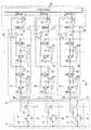
まず、画像形成装置(例えばプリンタ)のヘッド部に採用される電気光学装置の形態を説明する。図1は、この電気光学装置の構成を示す回路図である。同図に示されるように、電気光学装置D1は、画素部10とパルス出力回路20とデータ出力制御回路30とを有する。画素部10は、ライン型の光ヘッドとして利用される部分であり、各々がOLED素子15を含むn個の画素回路Pが一列に配列された構成となっている。各画素回路Pは、OLED素子15の点灯および消灯を制御するための回路であり、画素回路Pの配列と直交するように形成されたデータ線45に接続される。なお、図1においては第(j−1)列目から第(j+1)列目の要素のみが図示されているが、その他の各列に関わる要素も同様の構成である(jは2≦j≦n−1を満たす自然数)。
<A-1: First Embodiment>
First, the form of an electro-optical device employed in the head portion of an image forming apparatus (for example, a printer) will be described. FIG. 1 is a circuit diagram showing the configuration of the electro-optical device. As shown in the figure, the electro-optical device D1 includes a
各画素回路Pは、ソース電極が陽極側電源線51に接続されたpチャネル型のトランジスタ11と、ソース電極が陰極側電源線53に接続されたnチャネル型のトランジスタ12とを含む。各トランジスタ11,12のドレイン電極は相互に接続され、各々のゲート電極はデータ線45に対して共通に接続される。OLED素子15は、その陽極がトランジスタ12のドレイン電極に接続されるとともに陰極がトランジスタ12のソース電極に接続される。陽極側電源線51には電源回路(図示略)によって生成された発光用電源電位VHHelが供給され、陰極側電源線53には発光用電源電位VHHelよりも低い発光用電源電位VLLelが電源回路から供給される。この構成において、データ線45の電圧Dout(Dout[1]、Dout[2]、……、Dout[n]がトランジスタ11をオン状態とするローレベルになると、陽極側電源線51からOLED素子15を介して陰極側電源線53に電流が流れ、これによってOLED素子15は発光する。一方、データ線45の電圧Doutがトランジスタ12をオン状態とするハイレベルであれば、トランジスタ11がオフ状態となってOLED素子15への電流の供給が停止されるから、OLED素子15は消灯する。このようにOLED素子15の階調(発光および消灯)はデータ線45の電圧Doutに応じて制御される。
Each pixel circuit P includes a p-
パルス出力回路20およびデータ出力制御回路30は、信号線40に供給される階調信号Dgに応じて各データ線45の電圧Doutを制御する手段である。この階調信号Dgは、各OLED素子15の階調をその配列の順番に時分割にて指定する電圧信号である。本実施形態における階調信号Dgは、予め定められた単位時間ごとに、ひとつのOLED素子15の発光を指示するローレベルおよび消灯を指示するハイレベルの何れかとなる。
The
パルス出力回路20は、各々が順番にアクティブレベルとなるn系統のサンプリングパルスSMP(SMP[1]、SMP[2]、……、SMP[n]を出力する手段である。第j系統のサンプリングパルスSMP[j]は、第j段目のOLED素子15の階調を指定するために階調信号Dgを信号線40から取り込む期間(以下「サンプリング期間」という)を規定する信号である。
The
図1に示されるように、パルス出力回路20は、シフトレジスタ21とn個のAND回路22とを有する。シフトレジスタ21は、データ線45の総数に相当するn個の単位シフト回路(図示せず)を縦続接続して構成され、主走査期間の最初に供給される開始パルスをクロック信号に同期してシフトすることによってn系統のパルス信号SRout(SRout[1]、SRout[2]、……、SRout[n])を順次に出力する。各パルス信号SRoutは、クロック信号の1周期に相当する時間長だけアクティブレベルとなる信号である。また、図2に示されるように、各パルス信号SRout[j](jは1≦j≦nを満たす自然数)がアクティブレベルとなる期間と、その次段のパルス信号SRout[j+1]がアクティブレベルとなる期間とは、クロック信号の半周期に相当する時間長だけ重複する。
As shown in FIG. 1, the
各AND回路22は、時間的に前後してアクティブレベルとなる2系統のパルス信号SRoutの論理積を演算してサンプリングパルスSMP(SMP[1]、SMP[2]、……、SMP[n])を生成する回路である。例えば、第j段目のAND回路22は、第j番目のパルス信号SRout[j]とその直後の第(j+1)番目のパルス信号SRout[j+1]との論理積に相当するサンプリングパルスSMP[j]を出力する。したがって、図2に示されるように、パルス出力回路20から出力されるn系統のサンプリングパルスSMP[1]ないしSMP[n]は、各々のアクティブレベルとなる期間が相互に重複することなくサンプリング期間ごとに順番にアクティブレベルとなる。
Each AND
次に、図1に示されるデータ出力制御回路30は、各サンプリングパルスSMP[1]ないしSMP[n]に基づいて階調信号Dgを各データ線45にサンプリングする手段であり、各々がデータ線45に対応するn個の単位回路Uを有する。なお、以下では第j段目の単位回路Uの構成を説明するが、他の単位回路Uも同様の構成である。
Next, the data
各単位回路UはトランスミッションゲートG1を有する。総ての単位回路UにおけるトランスミッションゲートG1の入力端子は信号線40に対して共通に接続される。第j段目の単位回路UのトランスミッションゲートG1は、第j段目のAND回路22から出力されるサンプリングパルスSMP[j]に基づいて階調信号Dg(第j段目のOLED素子15の階調を指定する区間)をサンプリングするスイッチング素子である。すなわち、トランスミッションゲートG1は、サンプリングパルスSMP[j]とその論理レベルをインバータ32によって反転した信号とがアクティブレベルとなる期間にてオン状態(すなわち出力端子が信号線40に導通する状態)となる。
Each unit circuit U has a transmission gate G1. The input terminals of the
トランスミッションゲートG1の出力端子にはラッチ回路34が接続される。このラッチ回路34は、出力端子Na[j]がトランスミッションゲートG1の出力端子に接続されたクロックドインバータ341と、入力端子がクロックドインバータ341の出力端子Na[j]に接続されるとともに出力端子Nb[j]がクロックドインバータ341の入力端子に接続されたインバータ342とを有する。クロックドインバータ341の各制御端子には、シフトレジスタ21から出力されたパルス信号SRout[j]とその論理レベルをインバータ33によって反転させた信号とが供給される。このクロックドインバータ341は、パルス信号SRout[j]がアクティブレベル(ハイレベル)を維持する期間にてハイインピーダンス状態となり、パルス信号SRout[j]が非アクティブレベル(ローレベル)を維持する期間においてはインバータとして機能する。したがって、ラッチ回路34は、トランスミッションゲートG1が取り込んだ階調信号Dgをパルス信号SRout[j]が非アクティブレベルとなる期間にてラッチして出力端子Nb[j]に出力する。
A
ラッチ回路34の出力端子(すなわちインバータ342の出力端子)Nb[j]にはトランスミッションゲートG2の入力端子が接続される。このトランスミッションゲートG2は、トランスミッションゲートG1とデータ線45との間に介在し、データ線45に対する階調信号Dg(トランスミッションゲートG1が第j列目のOLED素子15のためにサンプリングした区間)の出力の許否を切り替えるためのスイッチング素子として機能する。このトランスミッションゲートG2の各制御端子には、クロックドインバータ341と同様に、パルス信号SRout[j]とその論理レベルを反転させた信号とが供給される。このパルス信号SRout[j]が非アクティブレベル(ローレベル)を維持する期間においては、トランスミッションゲートG2がオン状態(導通状態)となってデータ線45に対する階調信号Dgの供給が許可される一方、パルス信号SRout[j]がアクティブレベル(ハイレベル)を維持する期間においては、トランスミッションゲートG2がオフ状態(非導通状態)となってデータ線45に対する階調信号Dgの供給が停止される。オン状態となったトランスミッションゲートG2から出力された階調信号Dgは、出力インバータ35によって論理レベルが反転されたうえで第j列目のデータ線45に出力される。この出力インバータ35はデータ出力制御回路30の出力バッファとして機能する。
The input terminal of the transmission gate G2 is connected to the output terminal of the latch circuit 34 (that is, the output terminal of the inverter 342) Nb [j]. The transmission gate G2 is interposed between the transmission gate G1 and the
図1に示されるように、各単位回路UはキャパシタCを有する。このキャパシタCは、トランスミッションゲートG2の出力端子(出力インバータ35の入力端子)の電圧を保持するための容量であり、一端がトランスミッションゲートG2の出力端子に接続されるとともに他端が接地される。トランスミッションゲートG2がオフ状態にあるとき、データ線45の電圧Dout[j]は、その直前にトランスミッションゲートG2がオン状態となったときにキャパシタCに保持された論理レベルを出力インバータ35によって反転したレベルに保持される。
As shown in FIG. 1, each unit circuit U has a capacitor C. The capacitor C is a capacitor for holding the voltage of the output terminal of the transmission gate G2 (the input terminal of the output inverter 35), and one end is connected to the output terminal of the transmission gate G2 and the other end is grounded. When the transmission gate G2 is in the off state, the voltage Dout [j] of the
次に、本実施形態に係る電気光学装置D1の動作を説明する。ただし、以下では、図2に示されるタイミングT1ないしT4の各々における第j段目の単位回路Uの状態に特に注目し、他の単位回路Uの動作の説明は適宜に省略する。なお、タイミングT1においてキャパシタCにハイレベルが保持されている場合(すなわちデータ線45の電圧Dout[j]がローレベルに維持されて第j段目のOLED素子15が点灯している場合)を想定する。さらに、説明の便宜のために、第j段目を含む奇数段目のOLED素子15について消灯が指示され、偶数段目のOLED素子15について点灯が指示されるものとする。したがって、階調信号Dgは、図2に示されるように、単位時間(サンプリング期間と同じ時間長の期間)ごとに交互にハイレベルおよびローレベルの一方から他方に切り替わる。
Next, the operation of the electro-optical device D1 according to this embodiment will be described. However, in the following, particular attention is paid to the state of the j-th stage unit circuit U at each of the timings T1 to T4 shown in FIG. 2, and description of the operation of the other unit circuits U will be omitted as appropriate. Note that the case where the high level is held in the capacitor C at the timing T1 (that is, the case where the voltage Dout [j] of the
(1)タイミングT1
タイミングT1においては、シフトレジスタ21から出力されるパルス信号SRout[j]がローレベルを維持するため、AND回路22から出力されるサンプリングパルスSMP[j]もローレベルとなる。したがって、トランスミッションゲートG1はオフ状態となり、信号線40に供給されている階調信号Dgは第j段目の単位回路Uに取り込まれない。なお、このタイミングT1において、ラッチ回路34のクロックドインバータ341はオン状態となってインバータとして機能するとともに、トランスミッションゲートG2がオン状態となってラッチ回路34の出力端子Nb[j]は出力インバータ35の入力端子に導通する。
(1) Timing T1
At timing T1, since the pulse signal SRout [j] output from the
(2)タイミングT2
タイミングT2においては、パルス信号SRout[j]がハイレベルに遷移する。したがって、ラッチ回路34のクロックドインバータ341がハイインピーダンス状態になるとともに、トランスミッションゲートG2がオフ状態となってラッチ回路34の出力端子Nb[j]は出力インバータ35の入力端子から電気的に切り離される。このとき、キャパシタCに保持される論理レベルはハイレベルに維持されるから、第j列目のデータ線45の電圧Dout[j]はローレベルに維持される。なお、このタイミングT2においてパルス信号SRout[j+1]はローレベルに維持されているから、サンプリングパルスSMP[j]はローレベルに維持されてトランスミッションゲートG1はオフ状態を維持する。したがって、信号線40に供給されている階調信号Dgは第j段目の単位回路Uに取り込まれない。
(2) Timing T2
At timing T2, the pulse signal SRout [j] transitions to a high level. Therefore, the clocked
(3)タイミングT3
タイミングT3においては、パルス信号SRout[j]およびパルス信号SRout[j+1]の双方がハイレベルとなるから、これらの論理積であるサンプリングパルスSMP[j]がハイレベルとなってトランスミッションゲートG1はオン状態に遷移する。このサンプリングパルスSMP[j]がハイレベルとなるサンプリング期間においては、信号線40に供給される階調信号DgがトランスミッションゲートG1を介してラッチ回路34の入力端子Na[j]に供給される。ただし、ハイレベルのパルス信号SRout[j]によってクロックドインバータ341はハイインピーダンス状態となっているから、クロックドインバータ341およびインバータ342はラッチとしては機能しない。
(3) Timing T3
At timing T3, both the pulse signal SRout [j] and the pulse signal SRout [j + 1] are at a high level, so that the sampling pulse SMP [j], which is the logical product of these signals, is at a high level and the transmission gate G1. Transitions to the on state. During the sampling period when the sampling pulse SMP [j] is at a high level, the gradation signal Dg supplied to the
ここで、階調信号Dgが所期のタイミングから遅延していないとすれば、図2に示されるように、この階調信号DgはサンプリングパルスSMP[1]ないしSMP[n]のレベルが遷移するタイミングにて各OLED素子15の階調に応じたレベルに遷移する。しかしながら、階調信号Dgには信号線40における電圧降下や波形の鈍りといった種々の原因によって遅延が生じ得る。本実施形態においては、図2に「Dg(遅延あり)」として示されるように、階調信号Dgが所期のタイミングよりも時間長Δdだけ遅延した場合を想定する。このように遅延した階調信号DgがトランスミッションゲートG1を介して信号線40から取り込まれるため、サンプリング期間における入力端子Na[j]の電圧は、図2に示されるように、本来ならば当該サンプリング期間の始点から終点までローレベルに維持されるべきであるにも拘わらず、サンプリング期間の始点から時間長Δdが経過するまでの期間においてハイレベルとなる。そして、ラッチ回路34の出力端子Nb[j]の電圧はサンプリング期間の始点から時間長Δdが経過するまでの期間においてローレベルとなる。したがって、この出力端子Nb[j]の論理レベルを出力インバータ35によって反転したレベルがそのままデータ線45に印加されるとすれば、本来ならばローレベル(OLED素子15を発光させるレベル)に維持されるべきデータ線45の電圧が時間長Δdの期間にてハイレベルに遷移し、この結果として当該期間ではOLED素子15が消灯することになる。この輝度の誤差(ここでは輝度の低下)がゴーストの原因となるのである。
Here, if the gradation signal Dg is not delayed from the intended timing, the gradation signal Dg has a transition in the level of the sampling pulses SMP [1] to SMP [n] as shown in FIG. At a timing to make a transition to a level corresponding to the gradation of each
これに対し、本実施形態においては、図2に示されるように、タイミングT3においてハイレベルに維持されるパルス信号SRout[j]によってトランスミッションゲートG2はオフ状態に維持されているから、トランスミッションゲートG1によって取り込まれた階調信号DgはトランスミッションゲートG2の入力端子までしか到達せずデータ線45には出力されない。したがって、データ線45の電圧Dout[j]は、その時点でキャパシタCに保持されているハイレベルを出力インバータ35によって反転したローレベルに維持され、実際には階調信号Dgの遅延に起因して出力端子Nb[j]の電圧が変動しているにも拘わらずその影響はデータ線45の電圧に現れない。すなわち、データ線45の電圧Dout[j]は所期のレベル(ここではローレベル)に維持され、この結果としてOLED素子15はサンプリング期間の始点から終点までにわたって点灯することになる。したがって、階調信号Dgの遅延に起因したゴーストは発生しない。
On the other hand, in this embodiment, as shown in FIG. 2, the transmission gate G2 is maintained in the OFF state by the pulse signal SRout [j] maintained at the high level at the timing T3. The gradation signal Dg captured by the signal reaches only the input terminal of the transmission gate G2 and is not output to the
(4)タイミングT4
シフトレジスタ21から出力されるパルス信号SRout[j]がタイミングTaにてローレベルに遷移すると、クロックドインバータ341がオン状態となってインバータとして機能し始めるとともにトランスミッションゲートG2がオン状態となってラッチ回路34の出力端子Nb[j]が出力インバータ35の入力端子に導通する。このタイミングTaにおいてトランスミッションゲートG1によって取り込まれていた階調信号Dgはラッチ回路34によってラッチされたうえでトランスミッションゲートG2と出力インバータ35とを介してデータ線45に出力される。したがって、タイミングTaの経過後のタイミングT4においては、データ線45の電圧Dout[j]は所期の論理レベルであるローレベルに維持され、これによりトランジスタ11はオン状態となってOLED素子15が発光する。また、タイミングTaの経過後には、トランスミッションゲートG2の出力端子に接続されたキャパシタCにラッチ回路34の出力端子Nb[j]の論理レベルであるハイレベルが保持される。こうして階調信号Dgに応じた論理レベルがキャパシタCに保持されることにより、タイミングT2について説明したように、トランスミッションゲートG2(さらにはクロックドインバータ341)がオフ状態になってもデータ線45の電圧Dout[j]はローレベルに維持される。なお、タイミングTaの直後にサンプリングパルスSMP[j]はローレベルに維持するから、トランスミッションゲートG1がオフ状態となってラッチ回路34に対する階調信号Dgのサンプリングは停止される。
(4) Timing T4
When the pulse signal SRout [j] output from the
以上に説明したように、本実施形態においては、トランスミッションゲートG1によるサンプリングの開始から所定の期間が経過するまでトランスミッションゲートG2がオフ状態とされることによってデータ線45に対する階調信号Dgの供給が停止されるから、階調信号Dgの遅延に起因したデータ線45の電圧Doutの誤差を防止することができる。さらに、トランスミッションゲートG1の出力端子の電圧がキャパシタCによって保持されるから、トランスミッションゲートG1がオフ状態を維持する期間においてもデータ線45には所期の電圧Doutが印加される。したがって、本実施形態によれば、各データ線45に対して所期の電圧Doutを精度よく印加してゴーストの発生を防止することができる。
As described above, in this embodiment, the gradation signal Dg is supplied to the
ところで、階調信号Dgの遅延がデータ線45の電圧Doutに影響を与えないようにするための構成としては、図3に示される構成も考えられる。この構成においては、各単位回路UのトランスミッションゲートG2の後段にクロックドインバータ641とインバータ642とからなるラッチ回路64が配置される。そして、第j段目の単位回路UのトランスミッションゲートG2とラッチ回路64のクロックドインバータ641とは、パルス信号SRout[j]とその次段のパルス信号SRout[j+1]との論理和を反転した信号によってオン状態およびオフ状態の一方から他方に制御される。この構成においても、図4に示されるように、トランスミッションゲートG1がオン状態となって階調信号Dgが取り込まれる期間(NOR回路61の出力端子Nx[j]がローレベルとなる期間)では、トランスミッションゲートG2がオフ状態とされることによって信号線40とデータ線45とが電気的に切り離されるとともにその直前にラッチ回路64にラッチされた階調信号Dgがデータ線45に出力されるから、図1の構成と同様の効果が奏される。しかしながら、図3の構成においては、各単位回路UのトランスミッションゲートG2の後段にラッチ回路64が配置されることによってデータ出力制御回路30の構成の煩雑化(特に配線の引き回しの複雑化)や回路規模の肥大化を避けることができず、これに起因して電気光学装置D1の歩留まりの低下や製造コストの上昇を招くという問題がある。これに対し、本実施形態においては、トランスミッションゲートG2の後段にキャパシタCと出力インバータ35を配置すれば足りるから、図3の構成と比較してデータ出力制御回路30の構成の簡素化や回路規模の縮小が実現され、さらには電気光学装置D1の歩留まりの低下や製造コストの上昇といった問題も解消することができる。
By the way, as a configuration for preventing the delay of the gradation signal Dg from affecting the voltage Dout of the
<A−2:第1実施形態の変形例>
次に、第1実施形態を変形した態様について説明する。なお、以下に例示する各態様を適宜に組み合わせてもよい。また、以下の各態様のうち第1実施形態の各部と同様の要素については図1と共通の符号を付してその説明を適宜に省略する。
<A-2: Modification of First Embodiment>
Next, a modification of the first embodiment will be described. In addition, you may combine each aspect illustrated below suitably. Moreover, the same code | symbol as FIG. 1 is attached | subjected about the element similar to each part of 1st Embodiment among the following aspects, and the description is abbreviate | omitted suitably.
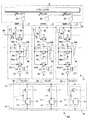
(1)第1の態様
図5は、第1実施形態を変形した第1の態様に係る電気光学装置D1の構成を示す回路図である。図1においては、キャパシタCの一端が接地された構成を例示したが、本態様に係る電気光学装置D1においては、電源の高位側電位Vddが供給される配線(以下「高位側電源線」という)と電源の低位側電位Vssが供給される配線(以下「低位側電源線」という)とにわたる配線にキャパシタCの一端が接続された構成となっている。高位側電位Vddおよび低位側電位Vssは、パルス出力回路20やデータ出力制御回路30の論理回路(特に出力インバータ35)の電源として利用される。高位側電源線と低位側電源線との間にはキャパシタC1が介挿され、一端がトランスミッションゲートG2に接続されたキャパシタCの他端はキャパシタC1のうち高位側電源線側(あるいは低位側電源線側であってもよい)の端部に接続されている。
(1) First Aspect FIG. 5 is a circuit diagram showing a configuration of an electro-optical device D1 according to a first aspect obtained by modifying the first embodiment. In FIG. 1, the configuration in which one end of the capacitor C is grounded is illustrated. However, in the electro-optical device D1 according to this aspect, a wiring (hereinafter referred to as a “higher power supply line”) to which the higher potential Vdd of the power supply is supplied. ) And a wiring to which the lower potential Vss of the power supply is supplied (hereinafter referred to as a “lower power supply line”), one end of the capacitor C is connected. The high potential Vdd and the low potential Vss are used as power sources for the logic circuits (particularly, the output inverter 35) of the
この構成によれば、高位側電源線に供給される高位側電位Vddや低位側電源線に供給される低位側電位Vssが何らかの原因(例えば他の論理回路における充放電)に起因して変動したとしても、この変動はキャパシタC1によって平滑化される。したがって、本態様によれば、各電源線の電位の変動に拘わらずデータ線45の電圧を安定させることができるという利点がある。さらに、出力インバータ35に電源を供給する高位側電源線または低位側電源線と、トランスミッションゲートG2の出力端子から出力インバータ35の入力端子に至る配線とを交差させることによってキャパシタCを形成することができるから、これらの配線とは別個の要素としてキャパシタCを配置する構成と比較して、データ出力制御回路30の回路規模を縮小することができる。
According to this configuration, the high potential Vdd supplied to the high power supply line and the low potential Vss supplied to the low power supply line fluctuate due to some cause (for example, charge / discharge in another logic circuit). However, this variation is smoothed by the capacitor C1. Therefore, according to this aspect, there is an advantage that the voltage of the
なお、ここではキャパシタCの一端が高位側電源線や低位側電源線に接続された構成を例示したが、これを他の配線に接続した構成も採用される。例えば、陽極側電源線51と陰極側電源線53とにキャパシタC1を介挿するとともにキャパシタCの一端を陽極側電源線51または陰極側電源線53に接続した構成としてもよい。この構成によれば、OLED素子15への電流の供給によって陽極側電源線51や陰極側電源線53の電位が変動した場合であってもキャパシタCの電圧を安定的に維持することができる。
Here, the configuration in which one end of the capacitor C is connected to the high-order power supply line or the low-order power supply line is illustrated, but a configuration in which this is connected to another wiring is also employed. For example, the
(2)第2の態様
図6は、第1実施形態を変形した第2の態様に係る電気光学装置D1の構成を示す回路図である。同図に示されるように、本態様における単位回路Uは、キャパシタCaとキャパシタCbとを有する。キャパシタCaは、一端がトランスミッションゲートG2の出力端子に接続されるとともに他端が陽極側電源線51に接続された容量であり、キャパシタCbは、一端がトランスミッションゲートG2の出力端子に接続されるとともに他端が陰極側電源線53に接続された容量である。この構成によれば、陽極側電源線51に供給される発光用電源電位VHHelおよび陰極側電源線53に供給される発光用電源電位VLLelの一方がOLED素子15の発光に伴って変動したとしても他方は安定的に維持されるから、キャパシタCaまたはCbに保持される電圧を安定させることができるという利点がある。また、トランスミッションゲートG2から出力インバータ35に至る配線を陽極側電源線51および陰極側電源線53と重ねるという簡易な構成によってキャパシタCaおよびCbを構成することができる。
(2) Second Aspect FIG. 6 is a circuit diagram showing a configuration of an electro-optical device D1 according to a second aspect obtained by modifying the first embodiment. As shown in the figure, the unit circuit U in this aspect includes a capacitor Ca and a capacitor Cb. The capacitor Ca is a capacitor having one end connected to the output terminal of the transmission gate G2 and the other end connected to the anode-
(3)第3の態様
図7は、第1実施形態を変形した第3の態様に係る電気光学装置D1の構成を示す回路図である。同図に示されるように、本態様においては、各単位回路UがOR回路36を有する。第j段目の単位回路UのOR回路36は、パルス出力回路20から当該単位回路Uに入力されるサンプリングパルスSMP[j]と、その直前にアクティブレベルとなるサンプリングパルスSMP[j-1]との論理和に相当する制御信号Sc[j]を出力する。各単位回路Uにおけるクロックドインバータ341およびトランスミッションゲートG2は、この制御信号Scによって制御される。制御信号Scは、図8に示されるように、パルス信号SRout[j]と略同一の波形となる。したがって、本態様によっても第1実施形態と同様の作用および効果が奏される。これに加え、本態様においては、シフトレジスタ21の出力の負荷が低減され、さらにはシフトレジスタ21の出力端子に関わる配線を簡素化することができるという利点がある。
(3) Third Aspect FIG. 7 is a circuit diagram showing a configuration of an electro-optical device D1 according to a third aspect obtained by modifying the first embodiment. As shown in the figure, in this embodiment, each unit circuit U has an
(4)第4の態様
図9は、第1実施形態を変形した第4の態様に係る電気光学装置D1の構成を示す回路図である。同図に示されるように、本態様においては、トランスミッションゲートG1と信号線40との間に遅延回路37が介挿される。この遅延回路37は、入力端子が信号線40に接続されたインバータ371と出力端子がトランスミッションゲートG1の入力端子に接続されたインバータ372とが直列に接続された回路である。トランスミッションゲートG1がオン状態に遷移すると、信号線40に供給される階調信号Dgは遅延回路37によって所定の時間長だけ遅延されたうえでラッチ回路34に入力される。一方、第j段目の単位回路Uに含まれるトランスミッションゲートG2とラッチ回路34のクロックドインバータ341とは、AND回路22から出力されたサンプリングパルスSMP[j]とその論理レベルをインバータ32によって反転させた信号とによってオン状態およびオフ状態の一方から他方に制御される。
(4) Fourth Aspect FIG. 9 is a circuit diagram showing a configuration of an electro-optical device D1 according to a fourth aspect obtained by modifying the first embodiment. As shown in the figure, in this embodiment, a
このようにトランスミッションゲートG1を制御するためのサンプリングパルスSMP[j]をトランスミッションゲートG2やクロックドインバータ341の制御のために兼用することにってデータ出力制御回路30の構成が簡素化される。さらに、シフトレジスタ21から出力されるパルス信号SRout[j]はトランスミッションゲートG2やクロックドインバータ341の制御に使用されないから、第3の態様と同様にシフトレジスタ21の出力の負荷を低減するとともにその出力端子に関わる配線を簡素化することができる。
Thus, the configuration of the data
ところで、このようにクロックドインバータ341をサンプリングパルスSMP[j]によって制御する構成においては、サンプリングパルスSMP[j]がローレベルに遷移してクロックドインバータ341がオン状態となった瞬間にトランスミッションゲートG1によって取り込まれている階調信号Dgがクロックドインバータ341とトランスミッションゲートG2とを介してデータ線45に出力される場合がある。したがって、階調信号Dgの時間軸上における誤差によっては、階調信号Dgのうち第j段目以外のOLED素子15の階調を指定する区間が第j段目のデータ線45に出力される可能性がある。これに対し、本態様によれば、トランスミッションゲートG1を介してラッチ回路34に取り込まれる階調信号Dgが遅延回路37によって遅延されているから、サンプリングパルスSMP[j]がアクティブレベルとなってトランスミッションゲートG2が完全にオフ状態となった後の段階で階調信号Dgの論理レベルが変動することになる。したがって、各データ線45に所期の電圧Dout[j]を精度よく印加することができるという利点がある。
By the way, in the configuration in which the clocked
<B−1:第2実施形態>
次に、本発明の第2実施形態に係る電気光学装置の構成を説明する。なお、本実施形態のうち第1実施形態やその変形例と同様の要素については共通の符号を付してその説明を適宜に省略する。
<B-1: Second Embodiment>
Next, the configuration of the electro-optical device according to the second embodiment of the invention will be described. In addition, the same code | symbol is attached | subjected about the element similar to 1st Embodiment and its modification among this embodiment, and the description is abbreviate | omitted suitably.
図10は、本実施形態に係る電気光学装置の構成を示す回路図である。同図に示されるように、この電気光学装置D2の各単位回路Uは、図1に示したトランスミッションゲートG2、出力インバータ35およびキャパシタCに代えてクロックドインバータ38を有する。さらに詳述すると、第j段目の単位回路Uに含まれるクロックドインバータ38は、入力端子がラッチ回路34の出力端子Nb[j]に接続されるとともに出力端子がデータ線45に接続される。そして、このクロックドインバータ38は、シフトレジスタ21から出力されるパルス信号SRout[j]がハイレベルとなる期間においてオフ状態(ハイインピーダンス状態)となり、パルス信号SRout[j]がローレベルとなる期間においてオン状態となってインバータとして機能する。すなわち、本実施形態におけるクロックドインバータ38は、第1実施形態におけるトランスミッションゲートG2および出力インバータ35の双方の役割に担うスイッチング素子として機能する。
FIG. 10 is a circuit diagram illustrating a configuration of the electro-optical device according to the present embodiment. As shown in the figure, each unit circuit U of the electro-optical device D2 includes a clocked
一方、本実施形態においても、クロックドインバータ38がオフ状態を維持する期間にてデータ線45の電圧Dout[j]を保持する容量(すなわち図1のキャパシタCに相当する容量)が必要となる。図10の構成においては、画素回路Pのトランジスタ11および12におけるゲート容量Cgがデータ線45の電圧Dout[j]を保持するための容量として利用される。すなわち、トランジスタ11やトランジスタ12のゲート・ソース間やゲート・ドレイン間にはゲート容量Cgが付随する。特に電気光学素子としてOLED素子15を適用した画素回路Pにおいては、このOLED素子15に充分な電流を供給するためにトランジスタ11や12のサイズは大きく、したがって各ゲート容量Cgはデータ線45の電圧Dout[j]を保持するために充分な容量を有する。
On the other hand, also in the present embodiment, a capacity for holding the voltage Dout [j] of the
これらのゲート容量Cgには、クロックドインバータ38がオン状態に遷移したときのデータ線45の電圧Dout[j]が保持され、クロックドインバータ38がオフ状態を維持する期間においてもデータ線45の電圧Dout[j]をそのままのレベルに維持する。したがって、本実施形態においても第1実施形態と同様の作用および効果が奏される。これに加えて、本実施形態においては、第1実施形態のトランスミッションゲートG2および出力インバータ35の代わりにひとつのクロックドインバータ38が利用されるから、図1の構成と比較してデータ出力制御回路30の回路規模を低減することができる。さらに、データ線45の電圧Dout[j]がゲート容量Cgによって保持されるから、第1実施形態のキャパシタCを不要とすることができ、この観点からしてもデータ出力制御回路30の回路規模を低減することができる。
These gate capacities Cg hold the voltage Dout [j] of the
<B−2:第2実施形態の変形例>
次に、第2実施形態を変形した態様について説明する。なお、以下に例示する各態様を適宜に組み合わせてもよい。また、以下の各態様のうち第1実施形態や第2実施形態の各部と同様の要素については図1や図10と共通の符号を付してその説明を適宜に省略する。
<B-2: Modification of Second Embodiment>
Next, a modification of the second embodiment will be described. In addition, you may combine each aspect illustrated below suitably. In addition, among the following aspects, the same elements as those in the first embodiment and the second embodiment are denoted by the same reference numerals as those in FIGS. 1 and 10, and the description thereof is omitted as appropriate.
(1)第1の態様
図10においてはデータ線45の電圧Doutをゲート容量Cgのみによって保持する構成を例示したが、クロックドインバータ38の出力端子に第1実施形態と同様のキャパシタCの一端を接続してもよい。さらに、図5や図6に示した構成を本実施形態に適用してもよい。例えば、図11に示されるように、電源の高位側電位Vddが供給される高位側電源線と低位側電位Vssが供給される低位側電源線とを連結する配線にキャパシタCの一端を接続した構成や、高位側電源線と低位側電源線との間に介挿されたキャパシタC1の一端にキャパシタCの一端を接続した構成も採用される。また、図12に示されるように、クロックドインバータ38の出力端子と陽極側電源線51との間にキャパシタCaが介挿された構成や、この出力端子と陰極側電源線53との間にキャパシタCbが介挿された構成も採用される。これらの態様によれば、データ出力制御回路30の構成が簡素化されるとともにデータ線45の電圧Doutを安定的に維持することができる。
(1) First aspect
Although FIG. 10 illustrates the configuration in which the voltage Dout of the
(2)第2の態様
図7に示した構成を第2実施形態に適用してもよい。すなわち、図13に示されるように、パルス信号SRout[j]とその前段のパルス信号SRout[j-1]との論理和に相当する制御信号Sc[j]をOR回路36によって生成し、この制御信号Sc[j]がハイレベルである期間にクロックドインバータ38をオフ状態に遷移させたり、制御信号Sc[j]がローレベルである期間にオン状態としてもよい。
(2) Second Mode The configuration shown in FIG. 7 may be applied to the second embodiment. That is, as shown in FIG. 13, the control signal Sc [j] corresponding to the logical sum of the pulse signal SRout [j] and the preceding pulse signal SRout [j-1] is generated by the
(3)第3の態様
図9に示した構成を第2実施形態に適用してもよい。すなわち、図14に示されるように、トランスミッションゲートG1と信号線40との間に遅延回路37を介挿するとともに、AND回路22から出力されるサンプリングパルスSMP[j]とその論理レベルを反転した信号とによってクロックドインバータ38を制御する構成としてもよい。
(3) Third Mode The configuration shown in FIG. 9 may be applied to the second embodiment. That is, as shown in FIG. 14, the
<C:電子機器>
各実施形態に例示した電気光学装置D(D1,D2)は各種の電子機器に使用される。本発明に係る電子機器の一例である画像形成装置の構成を以下に説明する。
<C: Electronic equipment>
The electro-optical device D (D1, D2) exemplified in each embodiment is used in various electronic apparatuses. A configuration of an image forming apparatus which is an example of an electronic apparatus according to the invention will be described below.
図15は、各実施形態に係る電気光学装置Dを利用した画像形成装置の構成を示す縦断側面図である。この画像形成装置は、同様な構成の4個の有機ELアレイ露光ヘッド20K、20C、20M、20Yを、対応する同様な構成である4個の感光体ドラム(像担持体)120K、120C、120M、120Yの露光位置にそれぞれ配置したものであり、タンデム方式の画像形成装置として構成されている。有機ELアレイ露光ヘッド20K、20C、20M、20Yは、各実施形態に係る電気光学装置Dの画素部10によって構成される。
FIG. 15 is a longitudinal side view illustrating a configuration of an image forming apparatus using the electro-optical device D according to each embodiment. This image forming apparatus includes four organic EL array exposure heads 20K, 20C, 20M, and 20Y having the same configuration and corresponding four photosensitive drums (image carriers) 120K, 120C, and 120M having the same configuration. , 120Y exposure positions, respectively, and is configured as a tandem image forming apparatus. The organic EL array exposure heads 20K, 20C, 20M, and 20Y are configured by the
図15に示すように、この画像形成装置は、駆動ローラ121と従動ローラ132が設けられており、図示矢印方向へ循環駆動される中間転写ベルト130を備えている。この中間転写ベルト130に対して所定間隔で配置された4個の像担持体としての外周面に感光層を有する120K、120C、120M、120Yが配置される。符号の後に付加されたK、C、M、Yはそれぞれ黒、シアン、マゼンタ、イエローを意味し、それぞれ黒、シアン、マゼンタ、イエロー用の感光体であることを示す。他の部材についても同様である。感光体120K、120C、120M、120Yは、中間転写ベルト130の駆動と同期して回転駆動される。
As shown in FIG. 15, the image forming apparatus includes a driving
各感光体120(K、C、M、Y)の周囲には、それぞれ感光体120(K、C、M、Y)の外周面を一様に帯電させる帯電手段(コロナ帯電器)211(K、C、M、Y)と、この帯電手段211(K、C、M、Y)により一様に帯電させられた外周面を感光体120(K、C、M、Y)の回転に同期して順次ライン走査する本発明の上記のような有機ELアレイ露光ヘッド20(K、C、M、Y)が設けられている。
また、この有機ELアレイ露光ヘッド20(K、C、M、Y)で形成された静電潜像に現像剤であるトナーを付与して可視像(トナー像)とする現像装置214(K、C、M、Y)を有している。
Around each photoconductor 120 (K, C, M, Y), charging means (corona charger) 211 (K) for uniformly charging the outer peripheral surface of the photoconductor 120 (K, C, M, Y), respectively. , C, M, Y) and the outer peripheral surface uniformly charged by the charging means 211 (K, C, M, Y) are synchronized with the rotation of the photoconductor 120 (K, C, M, Y). The organic EL array exposure head 20 (K, C, M, Y) as described above according to the present invention is sequentially provided.
Further, a developing device 214 (K) that applies toner as a developer to the electrostatic latent image formed by the organic EL array exposure head 20 (K, C, M, Y) to form a visible image (toner image). , C, M, Y).
ここで、各有機ELアレイ露光ヘッド20(K、C、M、Y)は、有機ELアレイ露光ヘッド20(K、C、M、Y)のアレイ方向が感光体ドラム120(K、C、M、Y)の母線に沿うように設置される。そして、各有機ELアレイ露光ヘッド20(K、C、M、Y)の発光エナルギーピーク波長と、感光体120(K、C、M、Y)の感度ピーク波長とは略一致するように設定されている。 Here, in each organic EL array exposure head 20 (K, C, M, Y), the array direction of the organic EL array exposure head 20 (K, C, M, Y) is the photosensitive drum 120 (K, C, M). , Y) along the bus. The light emission energy peak wavelength of each organic EL array exposure head 20 (K, C, M, Y) and the sensitivity peak wavelength of the photoconductor 120 (K, C, M, Y) are set to substantially coincide with each other. ing.
現像装置214(K、C、M、Y)は、例えば、現像剤として非磁性一成分トナーを用いるもので、その一成分現像剤を例えば供給ローラで現像ローラヘ搬送し、現像ローラ表面に付着した現像剤の膜厚を規制ブレードで規制し、その現像ローラを感光体120(K、C、M、Y)に接触あるいは押厚させることにより、感光体120(K、C、M、Y)の電位レベルに応じて現像剤を付着させることによりトナー像として現像するものである。 The developing device 214 (K, C, M, Y) uses, for example, a non-magnetic one-component toner as a developer, and the one-component developer is conveyed to the developing roller by a supply roller, for example, and adhered to the developing roller surface. The film thickness of the developer is regulated by a regulating blade, and the developing roller is brought into contact with or thickened on the photoconductor 120 (K, C, M, Y), whereby the photoconductor 120 (K, C, M, Y) The toner image is developed by attaching a developer according to the potential level.
このような4色の単色トナー像形成ステーションにより形成された黒、シアン、マゼンタ、イエローの各トナー像は、中間転写ベルト130上に順次一次転写され、中間転写ベルト130上で順次重ね合わされてフルカラーとなる。ピックアップローラ203によって、給紙カセット201から1枚ずつ給送された記録媒体202は、二次転写ローラ136に送られる。中間転写ベルト130上のトナー像は、二次転写ローラ136において用紙等の記録媒体202に二次転写され、定着部である定着ローラ対137を通ることで記録媒体202上に定着される。この後、記録媒体202は、排紙ローラ対138によって、装置上部に形成された排紙トレイ上へ排出される。
このように、図15の画像形成装置は、書き込み手段として有機ELアレイを用いているので、レーザ走査光学系を用いた場合よりも、装置の小型化を図ることができる。
The black, cyan, magenta, and yellow toner images formed by the four-color single-color toner image forming station are sequentially primary-transferred onto the
As described above, since the image forming apparatus of FIG. 15 uses the organic EL array as the writing means, the apparatus can be reduced in size as compared with the case where the laser scanning optical system is used.
次に、本発明に係る画像形成装置に係る他の実施の形態について説明する。
図16は、画像形成装置の縦断側面図である。図16において、画像形成装置には主要構成部材として、ロータリ構成の現像装置161、像担持体として機能する感光体ドラム165、有機ELアレイが設けられている露光ヘッド167、中間転写ベルト169、用紙搬送路174、定着器の加熱ローラ172、給紙トレイ178が設けられている。露光ヘッド167は上述した各実施形態に係る電気光学装置Dの画素部10によって構成されている。
現像装置161は、現像ロータリ161aが軸161bを中心として反時計回り方向に回転する。現像ロータリ161aの内部は4分割されており、それぞれイエロー(Y)、シアン(C)、マゼンタ(M)、ブラック(K)の4色の像形成ユニットが設けられている。現像ローラ162a〜162dおよびトナー供給ローラ163a〜163dは、4色の各像形成ユニットに各々配置されている。また、規制フレード164a〜164dによってトナーは所定の厚さに規制される。
Next, another embodiment of the image forming apparatus according to the present invention will be described.
FIG. 16 is a vertical side view of the image forming apparatus. In FIG. 16, the image forming apparatus includes, as main constituent members, a
In the developing
感光体ドラム165は、帯電器168によって帯電され、図示を省略した駆動モータ、例えばステップモータにより現像ローラ162aとは逆方向に駆動される。中間転写ベルト169は、従動ローラ170bと駆動ローラ170a間に張架されており、駆動ローラ170aが感光体ドラム165の駆動モータに連結されて、中間転写ベルトに動力を伝達している。当該駆動モータの駆動により、中間転写ベルト169の駆動ローラ170aは感光体ドラム165とは逆方向に回動される。
用紙搬送路174には、複数の搬送ローラと排紙ローラ対176などが設けられており、用紙を搬送する。中間転写ベルト169に担持されている片面の画像(トナー像)が、二次転写ローラ171の位置で用紙の片面に転写される。二次転写ローラ171は、クラッチにより中間転写ベルト169に離当接され、クラッチオンで中間転写ベルト169に当接されて用紙に画像が転写される。
The
The
上記のようにして画像が転写された用紙は、次に、定着ヒータを有する定着器で定着処理がなされる。定着器には、加熱ローラ172、加圧ローラ173が設けられている。定着処理後の用紙は、排紙ローラ対176に引き込まれて矢印F方向に進行する。この状態から排紙ローラ対176が逆方向に回転すると、用紙は方向を反転して両面プリント用搬送路175を矢印G方向に進行する。用紙は、給紙トレイ178から、ピックアップローラ179によって1枚ずつ取り出されるようになっている。
用紙搬送路において、搬送ローラを駆動する駆動モータは、例えば低速のブラシレスモークが用いられる。また、中間転写ベルト169は色ずれ補正などが必要となるのでステップモータが用いられている。これらの各モータは、図示を省略している制御手段からの信号により制御される。
The sheet on which the image has been transferred as described above is then subjected to a fixing process by a fixing device having a fixing heater. The fixing device is provided with a
For example, a low-speed brushless smoke is used as a drive motor for driving the conveyance roller in the sheet conveyance path. The
図の状態で、イエロー(Y)の静電潜像が感光体ドラム165に形成され、現像ローラ162aに高電圧が印加されることにより、感光体ドラム165にはイエローの画像が形成される。イエローの裏側および表側の画像がすべて中間転写ベルト169に担持されると、現像ロータリ161aが90度回転する。
中間転写ベルト169は1回転して感光体ドラム165の位置に戻る。次にシアン(C)の2面の画像が感光体ドラム165に形成され、この画像が中間転写ベルト169に担持されているイエローの画像に重ねて担持される。以下、同様にして現像ロータリ161の90度回転、中間転写ベルト169への画像担持後の1回転処理が繰り返される。
In the state shown in the drawing, a yellow (Y) electrostatic latent image is formed on the
The
4色のカラー画像担持には中間転写ベルト169は4回転して、その後に更に回転位置が制御されて二次転写ローラ171の位置で用紙に画像を転写する。給紙トレイ178から給紙された用紙を搬送路174で搬送し、二次転写ローラ171の位置で用紙の片面にカラー画像を転写する。片面に画像が転写された用紙はのように排紙ローラ対176で反転されて、搬送径路で待機している。その後、用紙は適宜のタイミングで二次転写ローラ171の位置に搬送されて、他面にカラー画像が転写される。ハウジング180には、排気ファン181が設けられている。
For carrying four color images, the
なお、上述した電気光学装置Dを画像読取装置に適用してもよい。この画像読取装置は、対象物に光線を照射する発光部と、対象物によって反射された光線を読み取って画像信号を出力する読み取り部とを備え、上述した電気光学装置Dを発光部に用いたことを特徴とする。ここで、発光部が移動して読み取り部が固定であってもよいし、発光部と読み取り部が一体となって移動するもであってもよい。後者の場合には、読み取り部をTFTで構成し、読み取り部と発光部を1枚の基板上に形成してもよい。このような画像読取装置としては、スキャナやバーコードリーダーが該当する。 The electro-optical device D described above may be applied to an image reading device. This image reading apparatus includes a light emitting unit that irradiates a light beam on an object and a reading unit that reads a light beam reflected by the object and outputs an image signal, and uses the electro-optical device D described above as a light emitting unit. It is characterized by that. Here, the light emitting unit may move and the reading unit may be fixed, or the light emitting unit and the reading unit may move together. In the latter case, the reading unit may be constituted by a TFT, and the reading unit and the light emitting unit may be formed on a single substrate. Examples of such an image reading apparatus include a scanner and a barcode reader.
なお、本発明に係る電気光学装置が適用される電子機器は画像形成装置や画像読取装置に限定されない。例えば、各種の電子機器における表示デバイスとして各実施形態に係る電気光学装置を利用してもよい。このような電子機器としては、パーソナルコンピュータ、携帯電話機、携帯型情報端末(PDA:Personal Digital Assistants)、デジタルスチルカメラ、テレビ、ビデオカメラ、カーナビゲーション装置、ページャ、電子手帳、電子ペーパー、電卓、ワードプロセッサ、ワークステーション、テレビ電話、POS端末、プリンタ、スキャナ、複写機、ビデオプレーヤ、タッチパネルを備えた機器等などが挙げられる。 The electronic apparatus to which the electro-optical device according to the invention is applied is not limited to an image forming apparatus or an image reading apparatus. For example, the electro-optical device according to each embodiment may be used as a display device in various electronic apparatuses. Such electronic devices include personal computers, mobile phones, personal digital assistants (PDAs), digital still cameras, televisions, video cameras, car navigation devices, pagers, electronic notebooks, electronic paper, calculators, word processors. , Workstations, videophones, POS terminals, printers, scanners, copiers, video players, devices with touch panels, and the like.
ところで、各実施形態においては画素回路Pが線状に配列された画素部10を例示したが、各種の電子機器の表示デバイスとしては多数の画素回路Pが面状に配列された電気光学装置が好適に採用される。図17は、この電気光学装置の構成を示すブロック図である。同図に示されるように、電気光学装置D3は、垂直走査回路(走査線駆動回路)Dyと水平走査回路(データ線駆動回路)Dxと表示部10aとを有する。水平走査回路Dxは、各実施形態に示したパルス出力回路20とデータ出力制御回路30とからなる。表示部10aには、X方向に延在して垂直走査回路Dyに接続された複数の走査線43と、Y方向に延在して水平走査回路Dxのデータ出力制御回路30(より具体的には第1実施形態における出力インバータ35や第2実施形態におけるクロックドインバータ38)に接続されたn本のデータ線45とが形成される。
By the way, in each embodiment, the
走査線43とデータ線45との各交差には画素回路P1が配置される。各画素回路P1は、nチャネル型のトランジスタTr1と、pチャネル型のトランジスタTr2と、キャパシタCcと、電気光学素子たるOLED素子15とを有する。トランジスタTr1は、ゲート電極が走査線43に接続されるとともにソース電極がデータ線45に接続される。トランジスタTr2は、ゲート電極がトランジスタTr1のドレイン電極に接続されるとともにソース電極が電源線に接続される。OLED素子15は、トランジスタTr2のドレイン電極に陽極が接続されるとともに陰極が接地される。キャパシタCcは、一端がトランジスタTr1のドレイン電極に接続される。
A
垂直走査回路Dyは、複数の走査線43の各々を順次に選択し、この選択した走査線43に対してトランジスタTr1をオン状態とする電圧を印加する。こうして1行分の画素回路PのトランジスタTr1が一斉にオン状態となった期間(水平走査期間)に、水平走査回路Dxによって各データ線45に印加された電圧DoutがキャパシタCcによって保持される。そして、この電圧Doutに応じてトランジスタTr2がオン状態またはオフ状態とされることによってOLED素子15に流れる電流が制御される。なお、ここではOLED素子15の挙動を制御するためのスイッチング素子(トランジスタTr1およびTr2)が画素回路P1に配置されたアクティブマトリクス方式の電気光学装置D3を例示したが、この種のスイッチング素子を持たないパッシブマトリクス方式の電気光学装置にも本発明は適用される。
The vertical scanning circuit Dy sequentially selects each of the plurality of
<D:その他の態様>
各実施形態においてはOLED素子15を利用した電気光学装置D(D1,D2,D3)を例示したが、これ以外の電気光学素子を利用した電気光学装置にも本発明は適用される。例えば、液晶を利用した液晶装置、無機EL素子を利用した電気光学装置、電界放出ディスプレイ(FED:Field Emission Display)、表面導電型電子放出ディスプレイ(SED:Surface-conduction Electron-emitter Display)、弾道電子放出ディスプレイ(BSD:Ballistic electron Surface emitting Display)、あるいは発光ダイオードを利用した表示装置など各種の電気光学装置にも本発明が適用される。
<D: Other aspects>
In each embodiment, the electro-optical device D (D1, D2, D3) using the
D1,D2,D3……電気光学装置、10……画素部、P,P1……画素回路、11,12……トランジスタ、15……OLED素子、20……パルス出力回路、21……シフトレジスタ、22……AND回路、32,33,342,371,372……インバータ、35……出力インバータ、34……ラッチ回路、30……データ出力制御回路、40……信号線、45……データ線、51……陽極側電源線、53……陰極側電源線、G1……トランスミッションゲート、G2……トランスミッションゲート、C,C1,Ca,Cb,Cc……キャパシタ、36……OR回路、37……遅延回路、341,38……クロックドインバータ。
D1, D2, D3 ... Electro-optical device, 10 ... Pixel part, P, P1 ... Pixel circuit, 11, 12 ... Transistor, 15 ... OLED element, 20 ... Pulse output circuit, 21 ... Shift register , 22 ... AND circuit, 32, 33, 342, 371, 372 ... inverter, 35 ... output inverter, 34 ... latch circuit, 30 ... data output control circuit, 40 ... signal line, 45 ...
Claims (13)
各々が順番にアクティブレベルとなる複数のサンプリングパルスを出力するパルス出力回路と、
各々に前記パルス出力回路からサンプリングパルスが供給される複数の単位回路と、
各電気光学素子の階調を順次に指定する階調信号が供給される信号線とを具備し、
前記各単位回路は、
前記信号線に供給される階調信号を前記パルス出力回路からのサンプリングパルスに応じてサンプリングする第1のスイッチング素子と、
前記第1のスイッチング素子と前記データ線との間に介挿され、当該第1のスイッチング素子によるサンプリングの開始から所定の期間が経過するまでオフ状態となる第2のスイッチング素子と、
前記第2のスイッチング素子の出力端子の電圧を保持する保持容量と
を有することを特徴とする駆動回路。 A drive circuit for driving an electro-optical device in which the gradation of the electro-optical element corresponding to each of the plurality of data lines is controlled according to the voltage of the data line;
A pulse output circuit for outputting a plurality of sampling pulses, each of which in turn becomes an active level;
A plurality of unit circuits each supplied with a sampling pulse from the pulse output circuit;
A signal line to which a gradation signal for sequentially specifying the gradation of each electro-optic element is supplied,
Each unit circuit is
A first switching element that samples a gradation signal supplied to the signal line according to a sampling pulse from the pulse output circuit;
A second switching element that is interposed between the first switching element and the data line and is turned off until a predetermined period has elapsed from the start of sampling by the first switching element;
And a holding capacitor for holding a voltage at an output terminal of the second switching element.
ことを特徴とする請求項1に記載の駆動回路。 The drive circuit according to claim 1, wherein the storage capacitor is a capacitive element having one end connected to an output terminal of the second switching element.
前記第1の電位供給線と前記第2の電位供給線との間に介挿された平滑用容量とを具備し、
前記保持容量の他端は、前記平滑用容量の一端に接続される
ことを特徴とする請求項2に記載の駆動回路。 First and second potential supply lines each supplied with a separate potential;
A smoothing capacitor interposed between the first potential supply line and the second potential supply line;
The drive circuit according to claim 2, wherein the other end of the holding capacitor is connected to one end of the smoothing capacitor.
前記第1および第2の電位供給線は、前記出力バッファに電源電位を供給する配線である
ことを特徴とする請求項3に記載の駆動回路。 An output buffer interposed between the second switching element and the data line;
The drive circuit according to claim 3, wherein the first and second potential supply lines are wirings for supplying a power supply potential to the output buffer.
前記各単位回路の第2のスイッチング素子は、前記シフトレジスタから出力されるパルス信号によって開閉が制御される
ことを特徴とする請求項1に記載の駆動回路。 The pulse output circuit includes a shift register that sequentially generates a plurality of pulse signals so that a period in which each pulse signal is at an active level and a period in which the next pulse signal is at an active level overlap each other, A logical product circuit that outputs a logical product of one pulse signal and the next pulse signal as a sampling pulse;
The driving circuit according to claim 1, wherein opening and closing of the second switching element of each unit circuit is controlled by a pulse signal output from the shift register.
前記第2のスイッチング素子は、前記論理和回路から出力される信号によって開閉が制御される
ことを特徴とする請求項1に記載の駆動回路。 Each unit circuit has a logical sum circuit that outputs a signal corresponding to the logical sum of the sampling pulse input to the unit circuit and the sampling pulse input to the unit circuit in the previous stage of the unit circuit,
The drive circuit according to claim 1, wherein the second switching element is controlled to be opened and closed by a signal output from the OR circuit.
前記各単位回路の第2のスイッチング素子は、前記パルス出力回路から出力されるサンプリングパルスによって開閉が制御される
ことを特徴とする請求項1に記載の駆動回路。 Each of the unit circuits has a delay element interposed between the signal line and the first switching element,
The driving circuit according to claim 1, wherein the second switching element of each unit circuit is controlled to be opened and closed by a sampling pulse output from the pulse output circuit.
ことを特徴とする請求項1に記載の駆動回路。 The drive circuit according to claim 1, wherein the second switching element is a transmission gate.
ことを特徴とする請求項1に記載の駆動回路。 2. The drive circuit according to claim 1, wherein the second switching element is a clocked inverter that has an output terminal in a high impedance state in an off state and functions as an inverter in an on state.
各々が順番にアクティブレベルとなる複数のサンプリングパルスを出力するパルス出力回路と、
各々に前記パルス出力回路からサンプリングパルスが供給される複数の単位回路と、
各電気光学素子の階調を順次に指定する階調信号が供給される信号線とを具備し、
前記各単位回路は、
前記信号線に供給される階調信号を前記パルス出力回路からのサンプリングパルスに応じてサンプリングする第1のスイッチング素子と、
前記第1のスイッチング素子と前記データ線との間に介挿され、当該第1のスイッチング素子によるサンプリングの開始から所定の期間が経過するまでオフ状態となる第2のスイッチング素子と、
前記第2のスイッチング素子の出力端子の電圧を保持する保持容量と
を有することを特徴とする電気光学装置。 A plurality of electro-optic elements arranged to correspond to each of the plurality of data lines and having gradation according to the voltage of the data line;
A pulse output circuit for outputting a plurality of sampling pulses, each of which in turn becomes an active level;
A plurality of unit circuits each supplied with a sampling pulse from the pulse output circuit;
A signal line to which a gradation signal for sequentially specifying the gradation of each electro-optic element is supplied,
Each unit circuit is
A first switching element that samples a gradation signal supplied to the signal line according to a sampling pulse from the pulse output circuit;
A second switching element that is interposed between the first switching element and the data line, and is turned off until a predetermined period has elapsed from the start of sampling by the first switching element;
An electro-optical device, comprising: a storage capacitor that holds a voltage of an output terminal of the second switching element.
前記保持容量は、一端が前記第2のスイッチング素子の出力端に接続されるとともに他端が前記第1の電源線に接続された第1の容量素子と、一端が前記第2のスイッチング素子の出力端に接続されるとともに他端が前記第2の電源線に接続された第2の容量素子とを含む
ことを特徴とする請求項10に記載の電気光学装置。 The electro-optic element is interposed between a first power supply line having a first potential and a second power supply line having a second potential different from the first potential,
The storage capacitor has one end connected to the output end of the second switching element and the other end connected to the first power supply line, and one end connected to the second switching element. The electro-optical device according to claim 10, further comprising: a second capacitive element connected to an output end and having the other end connected to the second power supply line.
前記各画素回路は、前記データ線を介してゲート電極に印加された電圧に応じて前記電気光学素子に印加される電圧を制御するトランジスタを含み、
前記保持容量は、前記トランジスタのゲート容量である
ことを特徴とする請求項10に記載の電気光学装置。 A plurality of pixel circuits each having the electro-optic element;
Each of the pixel circuits includes a transistor that controls a voltage applied to the electro-optic element in accordance with a voltage applied to the gate electrode via the data line,
The electro-optical device according to claim 10, wherein the storage capacitor is a gate capacitance of the transistor.
Priority Applications (5)
| Application Number | Priority Date | Filing Date | Title |
|---|---|---|---|
| JP2005011181A JP4385952B2 (en) | 2005-01-19 | 2005-01-19 | ELECTRO-OPTICAL DEVICE, DRIVE CIRCUIT THEREOF, AND ELECTRONIC DEVICE |
| US11/322,219 US7633480B2 (en) | 2005-01-19 | 2006-01-03 | Electro-optical device, driving circuit of electro-optical device, and electronic apparatus |
| TW095100646A TWI323870B (en) | 2005-01-19 | 2006-01-06 | Electro-optical device, and driving circuit of electro-optical device |
| KR1020060003737A KR100679967B1 (en) | 2005-01-19 | 2006-01-13 | Electro-optical device, driving circuit of electro-optical device, and electronic apparatus |
| CNB2006100059566A CN100498905C (en) | 2005-01-19 | 2006-01-17 | Electro-optical device, driving circuit of electro-optical device, and electronic apparatus |
Applications Claiming Priority (1)
| Application Number | Priority Date | Filing Date | Title |
|---|---|---|---|
| JP2005011181A JP4385952B2 (en) | 2005-01-19 | 2005-01-19 | ELECTRO-OPTICAL DEVICE, DRIVE CIRCUIT THEREOF, AND ELECTRONIC DEVICE |
Publications (2)
| Publication Number | Publication Date |
|---|---|
| JP2006198822A true JP2006198822A (en) | 2006-08-03 |
| JP4385952B2 JP4385952B2 (en) | 2009-12-16 |
Family
ID=36683343
Family Applications (1)
| Application Number | Title | Priority Date | Filing Date |
|---|---|---|---|
| JP2005011181A Expired - Fee Related JP4385952B2 (en) | 2005-01-19 | 2005-01-19 | ELECTRO-OPTICAL DEVICE, DRIVE CIRCUIT THEREOF, AND ELECTRONIC DEVICE |
Country Status (5)
| Country | Link |
|---|---|
| US (1) | US7633480B2 (en) |
| JP (1) | JP4385952B2 (en) |
| KR (1) | KR100679967B1 (en) |
| CN (1) | CN100498905C (en) |
| TW (1) | TWI323870B (en) |
Families Citing this family (7)
| Publication number | Priority date | Publication date | Assignee | Title |
|---|---|---|---|---|
| JP5130804B2 (en) * | 2006-10-02 | 2013-01-30 | セイコーエプソン株式会社 | Light emitting device and image forming apparatus |
| JP2010511342A (en) * | 2006-11-30 | 2010-04-08 | ノバトランス グループ エスエイ | Electrical devices that perform logical functions |
| JP5821685B2 (en) * | 2012-02-22 | 2015-11-24 | セイコーエプソン株式会社 | Electro-optical device and electronic apparatus |
| JP6102066B2 (en) * | 2012-03-13 | 2017-03-29 | セイコーエプソン株式会社 | Scanning line driving circuit, electro-optical device, and electronic apparatus |
| JP6957919B2 (en) * | 2017-03-23 | 2021-11-02 | セイコーエプソン株式会社 | Drive circuits and electronic devices |
| CN106920513B (en) | 2017-05-12 | 2019-09-24 | 京东方科技集团股份有限公司 | Driving circuit, display panel and the display device of display panel |
| CN107492353B (en) * | 2017-07-21 | 2019-06-11 | 惠科股份有限公司 | The driving method and driving device of display panel |
Citations (2)
| Publication number | Priority date | Publication date | Assignee | Title |
|---|---|---|---|---|
| JP2003202832A (en) * | 2001-09-17 | 2003-07-18 | Semiconductor Energy Lab Co Ltd | Method for driving light emitting device |
| JP2004077546A (en) * | 2002-08-09 | 2004-03-11 | Seiko Epson Corp | Output control circuit, driving circuit, electrooptical device, and electronic instrument |
Family Cites Families (17)
| Publication number | Priority date | Publication date | Assignee | Title |
|---|---|---|---|---|
| JPS61116334A (en) | 1984-11-09 | 1986-06-03 | Seiko Epson Corp | Active matrix panel |
| JP2562297B2 (en) | 1986-02-03 | 1996-12-11 | セイコーエプソン株式会社 | Driver-Built-in active matrix panel |
| JP3271192B2 (en) | 1992-03-02 | 2002-04-02 | ソニー株式会社 | Horizontal scanning circuit |
| JP2835254B2 (en) * | 1992-12-16 | 1998-12-14 | シャープ株式会社 | Display device drive circuit |
| US5818068A (en) * | 1994-09-22 | 1998-10-06 | Sharp Kabushiki Kaisha | Thin film transistor circuit and an active matrix type display device |
| JP3551600B2 (en) | 1996-01-30 | 2004-08-11 | セイコーエプソン株式会社 | Horizontal scanning circuit and liquid crystal display |
| JP4086925B2 (en) * | 1996-12-27 | 2008-05-14 | 株式会社半導体エネルギー研究所 | Active matrix display |
| JPH11214700A (en) * | 1998-01-23 | 1999-08-06 | Semiconductor Energy Lab Co Ltd | Semiconductor display device |
| US6268842B1 (en) * | 1998-04-13 | 2001-07-31 | Semiconductor Energy Laboratory Co., Ltd. | Thin film transistor circuit and semiconductor display device using the same |
| JP2000163014A (en) | 1998-11-27 | 2000-06-16 | Sanyo Electric Co Ltd | Electroluminescence display device |
| US6515648B1 (en) * | 1999-08-31 | 2003-02-04 | Semiconductor Energy Laboratory Co., Ltd. | Shift register circuit, driving circuit of display device, and display device using the driving circuit |
| TW525138B (en) * | 2000-02-18 | 2003-03-21 | Semiconductor Energy Lab | Image display device, method of driving thereof, and electronic equipment |
| US6989805B2 (en) * | 2000-05-08 | 2006-01-24 | Semiconductor Energy Laboratory Co., Ltd. | Light emitting device |
| JP2002108251A (en) | 2000-09-28 | 2002-04-10 | Sanyo Electric Co Ltd | Electro-luminescence display device |
| US6831299B2 (en) * | 2000-11-09 | 2004-12-14 | Semiconductor Energy Laboratory Co., Ltd. | Semiconductor device |
| JP2005128476A (en) * | 2003-04-17 | 2005-05-19 | Sanyo Electric Co Ltd | Display device |
| US7332936B2 (en) * | 2004-12-03 | 2008-02-19 | Semiconductor Energy Laboratory Co., Ltd. | Semiconductor circuit, display device, electronic apparatus |
-
2005
- 2005-01-19 JP JP2005011181A patent/JP4385952B2/en not_active Expired - Fee Related
-
2006
- 2006-01-03 US US11/322,219 patent/US7633480B2/en not_active Expired - Fee Related
- 2006-01-06 TW TW095100646A patent/TWI323870B/en not_active IP Right Cessation
- 2006-01-13 KR KR1020060003737A patent/KR100679967B1/en not_active IP Right Cessation
- 2006-01-17 CN CNB2006100059566A patent/CN100498905C/en not_active Expired - Fee Related
Patent Citations (2)
| Publication number | Priority date | Publication date | Assignee | Title |
|---|---|---|---|---|
| JP2003202832A (en) * | 2001-09-17 | 2003-07-18 | Semiconductor Energy Lab Co Ltd | Method for driving light emitting device |
| JP2004077546A (en) * | 2002-08-09 | 2004-03-11 | Seiko Epson Corp | Output control circuit, driving circuit, electrooptical device, and electronic instrument |
Also Published As
| Publication number | Publication date |
|---|---|
| KR20060084363A (en) | 2006-07-24 |
| US7633480B2 (en) | 2009-12-15 |
| US20060158395A1 (en) | 2006-07-20 |
| CN100498905C (en) | 2009-06-10 |
| CN1808550A (en) | 2006-07-26 |
| JP4385952B2 (en) | 2009-12-16 |
| TWI323870B (en) | 2010-04-21 |
| KR100679967B1 (en) | 2007-02-08 |
| TW200630933A (en) | 2006-09-01 |
Similar Documents
| Publication | Publication Date | Title |
|---|---|---|
| KR100787548B1 (en) | Pixel circuit, light-emitting device and electronic device | |
| US8125506B2 (en) | Electro-optical device and electronic apparatus | |
| JP4385952B2 (en) | ELECTRO-OPTICAL DEVICE, DRIVE CIRCUIT THEREOF, AND ELECTRONIC DEVICE | |
| KR20070075295A (en) | Electro-optical device, method of driving electro-optical device, and electronic apparatus | |
| KR100668274B1 (en) | Pixel circuit, light-emitting device, and image forming apparatus | |
| JP5211591B2 (en) | Data line driving circuit, electro-optical device, and electronic apparatus | |
| JP2007187706A (en) | Electrooptical apparatus, method for driving same, and electronic device | |
| JP4192987B2 (en) | Optical head, exposure apparatus, and image forming apparatus. | |
| JP2008205066A (en) | Light-emitting circuit, light-emitting device, image forming apparatus, display device, and driving method for light-emitting circuit | |
| JP2008055817A (en) | Electro-optic device, driving circuit, and electronic device | |
| JP2009063954A (en) | Data line driving circuit, electro-optical device, and electronic equipment | |
| JP4752412B2 (en) | Optical head, driving method thereof, and image forming apparatus | |
| JP4396693B2 (en) | Electro-optical device and electronic apparatus | |
| JP4552579B2 (en) | Light emitting device, driving method thereof, and image forming apparatus | |
| JP2007230004A (en) | Electro-optics apparatus and electronic instrument | |
| JP4259551B2 (en) | Electro-optical device, drive circuit, and electronic device | |
| JP2007253501A (en) | Drive circuit for light-emitting element, drive control method for the drive circuit, display unit equipped with the drive circuit for light-emitting element, and electric appliance equipped with the display unit | |
| JP2006076226A (en) | Light emitting apparatus, its driving method and image forming apparatus | |
| JP4702077B2 (en) | Electro-optical device and electronic apparatus | |
| JP2006095703A (en) | Light emitting device and driving method therefor and image forming device | |
| JP2008080608A (en) | Exposure head, image formation device, and exposure method | |
| JP2012076274A (en) | Drive circuit, optical print head, image forming device, and display device | |
| JP2008066433A (en) | Electro-optic device and electronic instrument | |
| JP2008126465A (en) | Electro-optic apparatus, electronic equipment, and image forming apparatus | |
| JP2007203565A (en) | Electrooptic device and electronic apparatus |
Legal Events
| Date | Code | Title | Description |
|---|---|---|---|
| RD04 | Notification of resignation of power of attorney |
Free format text: JAPANESE INTERMEDIATE CODE: A7424 Effective date: 20070404 |
|
| A977 | Report on retrieval |
Free format text: JAPANESE INTERMEDIATE CODE: A971007 Effective date: 20081114 |
|
| A131 | Notification of reasons for refusal |
Free format text: JAPANESE INTERMEDIATE CODE: A131 Effective date: 20081202 |
|
| A521 | Request for written amendment filed |
Free format text: JAPANESE INTERMEDIATE CODE: A523 Effective date: 20090128 |
|
| A02 | Decision of refusal |
Free format text: JAPANESE INTERMEDIATE CODE: A02 Effective date: 20090414 |
|
| A521 | Request for written amendment filed |
Free format text: JAPANESE INTERMEDIATE CODE: A523 Effective date: 20090615 |
|
| A911 | Transfer to examiner for re-examination before appeal (zenchi) |
Free format text: JAPANESE INTERMEDIATE CODE: A911 Effective date: 20090724 |
|
| TRDD | Decision of grant or rejection written | ||
| A01 | Written decision to grant a patent or to grant a registration (utility model) |
Free format text: JAPANESE INTERMEDIATE CODE: A01 Effective date: 20090908 |
|
| A01 | Written decision to grant a patent or to grant a registration (utility model) |
Free format text: JAPANESE INTERMEDIATE CODE: A01 |
|
| A61 | First payment of annual fees (during grant procedure) |
Free format text: JAPANESE INTERMEDIATE CODE: A61 Effective date: 20090921 |
|
| R150 | Certificate of patent or registration of utility model |
Free format text: JAPANESE INTERMEDIATE CODE: R150 |
|
| FPAY | Renewal fee payment (event date is renewal date of database) |
Free format text: PAYMENT UNTIL: 20121009 Year of fee payment: 3 |
|
| FPAY | Renewal fee payment (event date is renewal date of database) |
Free format text: PAYMENT UNTIL: 20121009 Year of fee payment: 3 |
|
| FPAY | Renewal fee payment (event date is renewal date of database) |
Free format text: PAYMENT UNTIL: 20131009 Year of fee payment: 4 |
|
| LAPS | Cancellation because of no payment of annual fees |