JP2006068252A - Game machine - Google Patents
Game machine Download PDFInfo
- Publication number
- JP2006068252A JP2006068252A JP2004254912A JP2004254912A JP2006068252A JP 2006068252 A JP2006068252 A JP 2006068252A JP 2004254912 A JP2004254912 A JP 2004254912A JP 2004254912 A JP2004254912 A JP 2004254912A JP 2006068252 A JP2006068252 A JP 2006068252A
- Authority
- JP
- Japan
- Prior art keywords
- integrated circuit
- input
- output
- main control
- terminal
- Prior art date
- Legal status (The legal status is an assumption and is not a legal conclusion. Google has not performed a legal analysis and makes no representation as to the accuracy of the status listed.)
- Pending
Links
Images


Abstract
Description
本発明は、遊技機に関し、特に、汎用性及び不正防止効果を高めた遊技機に関する。 The present invention relates to a gaming machine, and more particularly, to a gaming machine with improved versatility and fraud prevention effect.
遊技機、例えば、パチンコ機には、遊技機の動作を制御するための制御装置が複数設けられている。例えば、パチンコ機全体の動作を制御する主制御回路を有する主制御装置が設けられている。
主制御装置を構成する構成要素、例えば、主制御回路、記憶回路(ROMやRAM)、主制御回路と外部機器を接続するためのソケット等は、主制御基板に配置されている。各構成要素は、主制御基板に印刷されている配線パターン等の接続線によって接続されている。通常、主制御回路は、制御プログラム等を記憶している記憶回路(例えば、ROM)等とともに樹脂によってモールドされ、パッケージ化された主制御用集積回路(「ワンチップマイコン」という)として形成されている。各構成要素が配置された主制御基板は、内部が視認可能な透明性を有するケースに収納され、封印されている。
ところで、近年、遊技方法や遊技内容の複雑化や多様化に伴って、主制御回路とデータの入出力を行う外部機器(主制御基板に配置されている他の電気回路を含む)の数が増加し、また、主制御回路と外部機器との接続状態が変更されることが多くなっている。
外部機器の数が増加すると、既存の制御用集積回路に設けられているデータ端子(例えば、8個の端子によって構成される8ビットのデータ端子)の数が不足する場合がある。このような場合には、データ端子の数が多い主制御用集積回路を用いる必要がある。
また、主制御回路と外部機器との接続状態を変更する場合には、主制御用集積回路周辺の配線パターンを変更する必要がある。ここで、主制御回路は、遊技機全体の制御を行うため、多くの外部機器との間でデータの入出力を行っている。このため、主制御用集積回路周辺には多くの配線パターンが配設されており、主制御用集積回路周辺の配線パターンを変更するのは非常に困難である。
そこで、主制御用集積回路の汎用性を高め、外部機器の数の増加や主制御回路と外部機器との接続状態の変更に安価に対応できる技術の開発が要望されている。
ここで、主制御用集積回路の汎用性を高める方法として、入出力機能を拡張することができる入出力用集積回路(拡張I/Oポート機能を有する集積回路)を、主制御用集積回路と外部機器との間に設ける方法が考えられる。
この場合、主制御基板への入出力用集積回路の配置によって、他の電気回路の配置スペースが狭くなるため、主制御基板の実装効率を高める必要がある。
A gaming machine, for example, a pachinko machine, is provided with a plurality of control devices for controlling the operation of the gaming machine. For example, a main control device having a main control circuit that controls the operation of the entire pachinko machine is provided.
Components constituting the main control device, such as a main control circuit, a storage circuit (ROM and RAM), a socket for connecting the main control circuit and an external device, and the like are arranged on the main control board. Each component is connected by a connection line such as a wiring pattern printed on the main control board. Usually, the main control circuit is formed as a packaged main control integrated circuit (referred to as “one-chip microcomputer”) by molding with resin together with a storage circuit (for example, ROM) storing a control program and the like. Yes. The main control board on which each component is arranged is housed and sealed in a transparent case whose inside is visible.
By the way, in recent years, with the increasing complexity and diversification of game methods and game contents, the number of external devices (including other electric circuits arranged on the main control board) that input / output data with the main control circuit has increased. In addition, the connection state between the main control circuit and the external device is often changed.
When the number of external devices increases, the number of data terminals (for example, 8-bit data terminals constituted by eight terminals) provided in an existing control integrated circuit may be insufficient. In such a case, it is necessary to use a main control integrated circuit having a large number of data terminals.
Further, when changing the connection state between the main control circuit and the external device, it is necessary to change the wiring pattern around the main control integrated circuit. Here, the main control circuit inputs and outputs data with many external devices in order to control the entire gaming machine. Therefore, many wiring patterns are arranged around the main control integrated circuit, and it is very difficult to change the wiring patterns around the main control integrated circuit.
Accordingly, there is a demand for development of a technology that can increase the versatility of the main control integrated circuit and can cope with an increase in the number of external devices and a change in the connection state between the main control circuit and the external devices at low cost.
Here, as a method for improving the versatility of the main control integrated circuit, an input / output integrated circuit (an integrated circuit having an extended I / O port function) capable of expanding an input / output function is referred to as a main control integrated circuit. A method of providing it with an external device is conceivable.
In this case, since the arrangement space of other electric circuits is narrowed by the arrangement of the input / output integrated circuit on the main control board, it is necessary to improve the mounting efficiency of the main control board.
ところで、パチンコ機等の遊技機では、不正、特に、賞球数(遊技者に払い出される遊技球の数)を管理している主制御回路に対する不正が行われることが多い。
例えば、主制御用集積回路を不正な制御用集積回路(例えば、不正な制御プログラムを記憶しているROMを内蔵する制御用集積回路)に交換する不正が行われることがある。さらに、外観を正規の主制御用集積回路の外観に巧妙に似せた不正な制御用集積回路を用いる不正が行われることもある。この場合、このような不正を発見するのが困難である。
特に、主制御用集積回路としてDIP(Dual In-line Package)型(「横型」という)の集積回路を用いている場合、主制御基板(主制御基板の基板面)に対向する面(裏面)の面積が大きく、また、裏面と主制御基板との間の間隔が狭い。このため、主制御用集積回路が主制御基板に配置された状態では、ケースの外部から主制御用集積回路の裏面の状態を確認することができず、主制御用集積回路が不正な制御用集積回路に交換されたことや、主制御用集積回路と主制御基板との間に不正回路(例えば、不正な始動信号や入賞信号を出力する不正回路)が設けられていることを発見するのが困難である。
そこで、制御用集積回路としてZIP(Zig-zag In-line Package)型(「縦型」という)のROM内蔵の集積回路を用いた遊技機が提案されている。(特許文献1参)
縦型に形成された制御用集積回路は、制御用集積回路の面積が大きい表面及び裏面が基板の基板面から立ち上がる方向に配置されるため、ケースの外部から制御用集積回路の表面及び裏面の状態を容易に確認することができる。このため、制御用集積回路が不正な制御用集積回路に交換されたことや、制御用集積回路と基板の基板面との間に不正回路が設けられていることを容易に発見することができる。
また、縦型の形成された制御用集積回路は、基板に対向する面の面積が小さいため、基板の実装効率を高めることができる。
そこで、前記した、主制御用集積回路及び入出力用集積回路として、縦型の集積回路を用いることが考えられる。
For example, an illegal operation may be performed in which the main control integrated circuit is replaced with an unauthorized control integrated circuit (for example, a control integrated circuit incorporating a ROM storing an unauthorized control program). Further, fraud may be performed using an unauthorized control integrated circuit whose appearance is cleverly similar to that of a regular main control integrated circuit. In this case, it is difficult to find such fraud.
In particular, when a DIP (Dual In-line Package) type (“horizontal”) integrated circuit is used as the main control integrated circuit, the surface (back surface) facing the main control substrate (substrate surface of the main control substrate) And the distance between the back surface and the main control board is narrow. For this reason, in the state where the main control integrated circuit is arranged on the main control board, the state of the back surface of the main control integrated circuit cannot be confirmed from the outside of the case. To find out that an integrated circuit has been replaced, or that an unauthorized circuit (for example, an unauthorized circuit that outputs an unauthorized start signal or a winning signal) is provided between the main control integrated circuit and the main control board. Is difficult.
Therefore, a gaming machine using an integrated circuit with a built-in ROM of a ZIP (Zig-zag In-line Package) type (referred to as “vertical type”) has been proposed as an integrated circuit for control. (See Patent Document 1)
The control integrated circuit formed in a vertical shape is arranged in a direction in which the front and back surfaces of the control integrated circuit having a large area rise from the substrate surface of the substrate. The state can be easily confirmed. For this reason, it can be easily found that the control integrated circuit has been replaced with an unauthorized control integrated circuit, or that the unauthorized circuit is provided between the control integrated circuit and the substrate surface of the substrate. .
In addition, since the control integrated circuit formed in the vertical type has a small surface area facing the substrate, the mounting efficiency of the substrate can be increased.
Therefore, it is conceivable to use a vertical integrated circuit as the main control integrated circuit and the input / output integrated circuit.
主制御用集積回路と外部機器との間に入出力用集積回路を設けることにより、主制御用集積回路と外部機器との接続状態の変更や外部機器の数の増加等に対して安価に容易に対応することができ、主制御用集積回路の汎用性が向上する。
また、主制御用集積回路と入出力用集積回路としてZIP型(縦型)の制御用集積回路を用いることにより、主制御用集積回路に対する不正を防止することができるとともに、主制御基板の実装効率を高めることができる。
By providing an input / output integrated circuit between the main control integrated circuit and the external device, it is easy and inexpensive to change the connection state between the main control integrated circuit and the external device or increase the number of external devices. The versatility of the main circuit for integrated control is improved.
Further, by using a ZIP type (vertical type) control integrated circuit as the main control integrated circuit and the input / output integrated circuit, fraud to the main control integrated circuit can be prevented and the main control board can be mounted. Efficiency can be increased.
ところで、通常、基板に集積回路等の電気回路を配置する場合、電気回路を接続する接続線(通常は、基板に印刷されている配線パターン)の電気抵抗の増加による影響や接続線へのノイズの侵入を防止するために、接続線の長さが短くなるように電気回路が基板に配置される。
したがって、主制御用集積回路及び入出力用集積回路としてZIP型(縦型)の制御用集積回路を用いた場合にも、一般的には、主制御用集積回路と入出力用集積回路は、主制御用集積回路と入出力用集積回路の間の距離が短くなるように近づけて主制御基板に配置される。
ここで、主制御用集積回路には、識別情報を表示することが義務付けられている。このため、例えば、主制御用集積回路あるいは主制御用集積回路に内蔵されている主制御回路の型番を示す文字等が印刷されたラベルが主制御用集積回路に貼付されている。
ZIP型(縦型)の主制御用集積回路と入出力用集積回路が近づけて主制御基板に配置され、また、主制御用集積回路の、入出力用集積回路に対向する側の面にラベルが貼付されている場合には、入出力用集積回路の存在によって、主制御用集積回路に貼付されているラベルに印刷されている文字等をケースの外部から視認するのが困難となる。
この場合、主制御用集積回路が、外観は正規の主制御用集積回路の外観に巧妙に似せているが、正規のシールが貼付されていない不正な制御用集積回路に交換されたことを判別するのが困難となる。
そこで、本発明が解決しようとする課題は、不正防止効果を高めながら、制御用集積回路の汎用性を高めることができる遊技機を提供することである。
By the way, usually, when an electric circuit such as an integrated circuit is arranged on a substrate, the influence of an increase in electric resistance of a connection line (usually a wiring pattern printed on the substrate) connecting the electric circuit or noise to the connection line. In order to prevent the intrusion, the electric circuit is arranged on the substrate so that the length of the connection line is shortened.
Therefore, even when a ZIP type (vertical) control integrated circuit is used as the main control integrated circuit and the input / output integrated circuit, generally, the main control integrated circuit and the input / output integrated circuit are: The main control integrated circuit and the input / output integrated circuit are arranged close to each other on the main control board so as to shorten the distance.
Here, the main control integrated circuit is obliged to display identification information. For this reason, for example, a label printed with a character or the like indicating the model number of the main control circuit incorporated in the main control integrated circuit or the main control integrated circuit is attached to the main control integrated circuit.
The ZIP type (vertical type) main control integrated circuit and the input / output integrated circuit are arranged close to each other on the main control board, and the main control integrated circuit is labeled on the side facing the input / output integrated circuit. Is attached, it becomes difficult to visually recognize characters and the like printed on the label attached to the main control integrated circuit from the outside of the case due to the presence of the input / output integrated circuit.
In this case, it is determined that the main control integrated circuit has been replaced with an unauthorized control integrated circuit that has a similar appearance to that of a regular main control integrated circuit but does not have a proper seal. It becomes difficult to do.
Therefore, the problem to be solved by the present invention is to provide a gaming machine capable of enhancing the versatility of the control integrated circuit while enhancing the fraud prevention effect.
前記課題を解決するために、本発明の遊技機は、請求項1に記載された構成を備えている。
請求項1に記載の遊技機では、制御用構成要素と入出力用構成要素は、基板に最も近い面が最も大きい面積を有する面とならないように基板に配置されているとともに、制御用構成要素の、入出力用構成要素に対向する側の面に表示されている識別情報の視認が可能となるように離して平行に配置されている。
「基板に最も近い面が最も大きい面積を有する面とならないように基板に配置されている」という記載は、制御用構成要素及び入出力用構成要素が基板に配置された時に、基板に最も近い面(例えば、面の中心と基板面との間の距離が最も小さい面)の面積より大きい他の面が存在する配置態様を表している。この典型的な配置態様は、制御用構成要素及び入出力用構成要素としてZIP型等の縦型の制御用集積回路を用い、制御用構成要素が基板の基板面に配置された時に、制御用構成要素の最も面積が大きい面が、基板面から略直角に立ち上がるように配置される態様である。
「制御用構成要素に表示されている識別情報」は、例えば、制御用構成要素に印刷されているあるいは制御用構成要素に貼付されているラベルに印刷されている、当該制御用構成要素あるいは当該制御用構成要素に内蔵されている制御回路の型番を示す文字等の情報を含む。
「制御用構成要素と入出力用構成要素が平行に配置される」という記載は、制御用構成要素の端子列の配列方向と入出力用構成要素の端子列の配列方向が平行になるように、制御用構成要素と入出力用構成要素が配置される構成を意味する。なお、「平行に配置される」構成には、略平行に配置される構成も含まれる。
「制御用構成要素と入出力用構成要素が、制御用構成要素の、入出力用構成要素に対向する面に表示されている識別情報の視認が可能となるように離して平行に配置されている」構成としては、制御用構成要素に表示されている識別情報全体を視認可能な距離以上離して制御用構成要素と入出力用構成要素が平行に配置されている構成や、制御用構成要素に表示されている識別情報の一部を視認可能であり、且つ、視認した識別情報の一部に基づいて識別情報全体を推定可能な距離以上離して制御用構成要素と入出力用構成要素が平行に配置されている構成を用いることができる。すなわち、必ずしも、識別情報の全体を視認可能でなくてもよい。
In order to solve the above-described problems, a gaming machine according to the present invention has the configuration described in
In the gaming machine according to
The description that “the surface closest to the substrate is not disposed on the substrate so that it has the largest area” is the closest to the substrate when the control component and the input / output component are disposed on the substrate. This represents an arrangement mode in which another surface larger than the area of the surface (for example, the surface having the smallest distance between the center of the surface and the substrate surface) exists. In this typical arrangement mode, a vertical control integrated circuit such as a ZIP type is used as a control component and an input / output component, and when the control component is arranged on the substrate surface of the substrate, This is an aspect in which the surface having the largest area of the component is arranged so as to rise substantially perpendicularly from the substrate surface.
The “identification information displayed on the control component” is, for example, the control component or the relevant component printed on the label that is printed on the control component or attached to the control component. It includes information such as characters indicating the model number of the control circuit incorporated in the control component.
The description that “the control component and the input / output component are arranged in parallel” means that the arrangement direction of the terminal row of the control component and the arrangement direction of the terminal row of the input / output component are parallel. This means a configuration in which a control component and an input / output component are arranged. Note that the “arranged in parallel” configuration includes an approximately parallel configuration.
“The control component and the input / output component are arranged in parallel so that the identification information displayed on the surface of the control component facing the input / output component is visible. As the configuration, the control component and the input / output component are arranged in parallel, with the entire identification information displayed on the control component separated by a visible distance or more, or the control component A part of the identification information displayed on the control unit can be visually recognized, and the control component and the input / output component are separated by at least a distance that can be estimated based on a part of the recognized identification information. A configuration arranged in parallel can be used. That is, the entire identification information may not necessarily be visible.
請求項1に記載の遊技機では、制御用構成要素と外部機器との間に入出力用構成要素を設けているため、制御用構成要素と外部機器との接続状態の変更や外部機器の数の増加に対して安価に容易に対応することができ、制御用構成要素の汎用性が向上する。
また、制御用構成要素及び入出力用構成要素を、基板に最も近い面が最も大きい面積を有する面とならないように基板に配置しているため、基板の実装効率を高めることができるとともに、制御用構成要素や入出力用構成要素と基板の基板面との間に不正回路が設けられていることを容易に発見することができる。
さらに、制御用構成要素に表示されている識別情報の視認が可能となるように制御用構成要素と入出力用構成要素を離して基板に平行に配置しているため、不正な制御用構成要素(例えば、外観は正規の制御用構成要素に似せているが、正規の表示情報が表示されていない不正な制御用構成要素)が設けられていることを容易に発見することができ、不正防止効果を高めることができる。
ここで、制御用構成要素と入出力用構成要素を離して配置することにより、制御用構成要素と入出力用構成要素を接続する接続線の長さが長くなるが、制御用構成要素と入出力用構成要素を平行に配置しているため、接続線の長さが長くなる量を最小限に抑えることができる。
In the gaming machine according to
In addition, since the control component and the input / output component are arranged on the substrate so that the surface closest to the substrate is not the surface having the largest area, the mounting efficiency of the substrate can be improved and the control can be performed. It can be easily found that an unauthorized circuit is provided between the circuit component and the input / output component and the substrate surface of the substrate.
Furthermore, since the control component and the input / output component are arranged in parallel to the substrate so that the identification information displayed on the control component can be visually recognized, an illegal control component (For example, it is possible to easily find that an unauthorized control component that is similar in appearance to a regular control component but does not display regular display information) is provided, thus preventing fraud. The effect can be enhanced.
Here, by disposing the control component and the input / output component apart from each other, the length of the connection line connecting the control component and the input / output component is increased. Since the output components are arranged in parallel, the amount of increase in the length of the connection line can be minimized.
以下に、本発明の実施の形態を、図面を参照して説明する。
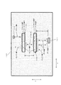
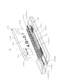
本発明の一実施の形態の遊技機に設けられる主制御基板の概略構成を示す図1に示す。また、図1のII線矢視図(矢印II方向から見た平面図)を図2に示し、図1の要部の斜視図を図3に示す。なお、図2に示されている構成要素(電気回路)の一部(例えば、発振器122)は、図1には示していない。また、図1及び図2には、主制御基板に配置される構成要素(電気回路)の全てを示していない。
本実施の形態では、パチンコ機に用いられている、主制御回路とROM等の記憶回路を内蔵する主制御用集積回路、入出力処理回路を内蔵する入出力用集積回路等が配置された主制御基板について説明する。
Embodiments of the present invention will be described below with reference to the drawings.
FIG. 1 shows a schematic configuration of a main control board provided in the gaming machine according to the embodiment of the present invention. Moreover, the II line arrow directional view (plan view seen from arrow II direction) of FIG. 1 is shown in FIG. 2, and the perspective view of the principal part of FIG. 1 is shown in FIG. Note that some of the components (electric circuits) shown in FIG. 2 (for example, the oscillator 122) are not shown in FIG. 1 and 2 do not show all the components (electrical circuits) arranged on the main control board.
In this embodiment, a main control integrated circuit incorporating a main control circuit and a storage circuit such as a ROM, an input / output integrated circuit incorporating an input / output processing circuit, etc. used in a pachinko machine are arranged. The control board will be described.
主制御基板120の一方側の基板面(実装側基板面)120aには、主制御用集積回路130、入出力用集積回路140、ソケット121、発振器122等が配置されている。
主制御用集積回路130、入出力用集積回路140、ソケット121、発振器122等の構成要素(電気回路)が配置された主制御基板120は、ベースとカバーからなるケース110内に収納され、封印具や封印シール等によって封印される。ケース110は、通常、ケース110が遊技機に取り付けられた状態で、係員等が、ケース外部からケース内部の状態(例えば、主制御基板120に配置されている構成要素の配置状態、構成要素の外形形状や構成要素に表示されている識別情報等)を視認可能な透明性を有する樹脂によって形成されている。
A main control integrated
A
主制御用集積回路(「CPUチップ」という)130は、主制御回路、ROM等の記憶回路、端子(データバス端子、セレクト端子、クロック端子等を含む)131が樹脂等によってモールドされて形成されている。主制御用集積回路130は、主制御基板120(主制御基板120の実装側基板面120a)に基も近い面(主制御基板120側に配置される面)が最も大きい面積を有する面とならないように主制御基板120(主制御基板120の実装側基板面120a)に配置される。
本実施の形態では、主制御用集積回路130として、ZIP型(縦型)に形成された制御用集積回路を用いている。主制御用集積回路130は、側面130a(入出力用集積回路140に対向する側の面)及び側面130b(入出力用集積回路140に対向する側と反対側の面)、底面(基板面120aに対向する面)130cを有している(図10参照)。側面130aあるいは130bが、面積が最も大きい面である。
長方形に形成されている底面130cには、長辺方向(図10では、紙面に垂直な方向)に端子131がジグザグ状に交互に配列されている。これにより、端子131の先端部によって、底面の長辺方向に平行な2列の直線状の端子列131a、131bが形成されている。
The main control integrated circuit (referred to as “CPU chip”) 130 is formed by molding a main control circuit, a storage circuit such as a ROM, and terminals (including a data bus terminal, a select terminal, a clock terminal, etc.) 131 with resin or the like. ing. The main control integrated
In the present embodiment, as the main control integrated
入出力用集積回路(「IOチップ」という)140は、入出力処理回路、端子(データバス端子、データ端子、セレクト端子を含む)141が樹脂等によってモールドされて形成されている。入出力用集積回路140は、主制御基板120(主制御基板120の実装側基板面120a)に基も近い面(主制御基板120側に配置される面)が最も大きい面積を有する面とならないように主制御基板120(主制御基板120の実装側基板面120a)に配置される。
本実施の形態では、入出力用集積回路140は、主制御用集積回路130と同様に、ZIP型(縦型)に形成された入出力用集積回路を用いており、側面140a及び140b、底面140c(図示省略)を有している。
長方形に形成されている底面140cには、長辺方向に端子141がジグザグ状に交互に配列されている。これにより、端子141の先端部によって、底面の長辺方向に平行な2列の直線状の端子列141a、141bが形成されている。
本実施の形態では、主制御用集積回路130及び入出力用集積回路140として、外形形状が同じであり、端子131と141の数及び配置形状が同じである集積回路を用いている。
An input / output integrated circuit (referred to as an “IO chip”) 140 is formed by molding an input / output processing circuit and terminals (including a data bus terminal, a data terminal, and a select terminal) 141 with resin or the like. The input / output integrated
In the present embodiment, the input / output integrated
On the bottom surface 140c formed in a rectangular shape, terminals 141 are alternately arranged in a zigzag shape in the long side direction. Thus, two rows of linear terminal rows 141 a and 141 b parallel to the long side direction of the bottom surface are formed by the tip portion of the terminal 141.
In this embodiment, as the main control integrated
本実施の形態の主制御回路が本発明の「制御回路」に対応し、主制御用集積回路130が本発明の「制御用構成要素」あるいは「制御用集積回路」に対応し、入出力用処理回路が本発明の「入出力用処理回路」に対応し、入出力用集積回路140が本発明の「入出力用構成要素」あるいは「入出力用集積回路」に対応し、主制御基板120が本発明の「制御基板」に対応する。
The main control circuit of this embodiment corresponds to the “control circuit” of the present invention, and the main control integrated
主制御基板120には、主制御用集積回路130の端子131が挿入可能(すなわち、接続可能)な主制御用挿入部(主制御用接続端子)120CPUと、入出力用集積回路140の端子141が挿入可能(すなわち、接続可能)な入出力用挿入部(入出力用接続端子)120IOが設けられている(図14参照)。
主制御用挿入部120CPUは、主制御用集積回路130の2列の端子列131a及び131bに対応させて配列された、平行な2列の主制御用挿入部列(主制御用接続端子列)120CPUa及び120CPUbを有している。
また、入出力用挿入部120IOは、入出力用集積回路140の2列の端子列141a及び141bに対応させて配列された、平行な2列の入出力用挿入部列(入出力用接続端子列)120IOa及び120IObを有している。
On the
The main control insertion portion 120CPU is arranged in parallel with the two rows of
The input / output insertion section 120IO includes two parallel input / output insertion section rows (input / output connection terminals) arranged in correspondence with the two terminal arrays 141a and 141b of the input / output integrated
本実施の形態では、主制御用集積回路130の端子131(端子列131a及び131bを形成)が本発明の「制御用集積回路の端子」に対応し、主制御用挿入部120CPU
(主制御用挿入部列120CPUa及び120CPUbを形成)が本発明の「制御用接続部」に対応し、入出力用集積回路140の端子141(端子列141a及び141bを形成)が本発明の「入出力用集積回路の端子」に対応し、入出力用挿入部120IO(入出力用挿入部列120IOa及び120IObを形成)が本発明の「入出力用接続部」に対応する。
In the present embodiment, the terminal 131 (forming the
(Forms the main control insertion row 120CPUa and 120CPUb) corresponds to the “control connection portion” of the present invention, and the terminal 141 of the input / output integrated circuit 140 (forms the terminal rows 141a and 141b) of the present invention. Corresponding to “terminal of input / output integrated circuit”, input / output insertion portion 120IO (forming input / output insertion portion rows 120IOa and 120IOb) corresponds to “input / output connection portion” of the present invention.
ここで、接続線の抵抗の影響や接続線へのノイズの侵入等の観点から、接続線はできるだけ短いほうが好ましい。
そこで、本実施の形態では、制御用挿入部120CPUの制御用挿入部列120CPUa及び120CPUbの配列方向と入出力用挿入部120IOの入出力用挿入部列120IOa及び120IObの配列方向が平行となるように、制御用挿入部120CPU及び入出力用挿入部120IOを基板120に配置することによって(すなわち、主制御用集積回路130の端子131の端子列131a及び131bの配列方向と入出力用集積回路140の端子列141a及び141bの配列方向を平行とすることによって)、制御用挿入部120と入出力用挿入部120IOの間(すなわち、主制御用集積回路130の端子131と入出力用集積回路140の端子141との間)に配設されるデータバスの長さを短くしている。本実施の形態では、このような配置状態を、「主制御用集積回路130と入出力用集積回路140が平行に制御基板120に配置されている」という。
本実施の形態では、主制御用集積回路130と入出力用集積回路140は、平行方向の配置位置が一致(略一致を含む)している、すなわち、平行方向にずれていない状態(ほとんどずれでいない状態を含む)で平行に配置されている。
Here, it is preferable that the connection line is as short as possible from the viewpoint of the influence of the resistance of the connection line and the intrusion of noise into the connection line.
Therefore, in this embodiment, the arrangement direction of the control insertion row 120CPUa and 120CPUb of the control insertion portion 120CPU and the arrangement direction of the input / output insertion row 120IOa and 120IOb of the input / output insertion portion 120IO are parallel to each other. In addition, the control insertion portion 120CPU and the input / output insertion portion 120IO are arranged on the substrate 120 (that is, the arrangement direction of the
In the present embodiment, the main control integrated
また、入出力用集積回路140に接続されるソケット121は、入出力用集積回路140と電気回路との間に配設される接続線の長さを短くするために、制御基板120の、入出力用集積回路140の配置方向に沿った両側に配置される。
そこで、本実施の形態では、主制御基板120の実装効率を高めるために、入出力用挿入部120IOの入出力用挿入部列120IOa及び120IObの配列方向(したがって、入出力用挿入部列120IOa及び120IObと平行な主制御用挿入部列120CPUa及び120CPUbの配列方向)が、主制御基板120の、長方形に形成されている基板面120aの長辺に平行(図2の左右方向)と平行になるように、入出力用挿入部120IO(したがって、制御用挿入部120CPU)を基板120に配置している、本実施の形態では、このような配置状態を、「主制御用集積回路130と入出力用集積回路140が基板120の基板面120aの長辺に平行に配置されている」という。
In addition, the socket 121 connected to the input / output integrated
Therefore, in the present embodiment, in order to increase the mounting efficiency of the
また、入出力用集積回路140には、ソケット121等の多くの電気回路が接続される。
そこで、本実施の形態では、図1及び図2に示すように、入出力用挿入部120IO(入出力用挿入部列120IOa及び120IOb)を、主制御用挿入部120CPU(主制御用挿入部列120CPUa及び120CPUb)よりも主制御基板120の基板面120aの中央部側に配置することによって、入出力用集積回路140と他の電気回路との間に配設される接続線の長さを短くしている。
さらに、ソケット121の接続端子の配列方向と入出力用挿入部列120OIa及び120IObの配列方向が平行となるように、ソケット121を制御基板120に取り付けているこのような配置状態を、「ソケット(接続部)を入出力用集積回路140と平行に配置する」という。
なお、本明細書では、「平行」という記載は、2つの構成要素が概略平行である構成をも含むものとして用いている。また、「中央部」という記載は、中央の位置の近傍を含むものとして用いている。
In addition, many electric circuits such as the socket 121 are connected to the input / output integrated
Therefore, in the present embodiment, as shown in FIGS. 1 and 2, the input / output insertion section 120IO (input / output insertion section row 120IOa and 120IOb) is replaced with the main control insertion section 120CPU (main control insertion section row). 120CPUa and 120CPUb) are arranged closer to the central portion of the board surface 120a of the
Further, such an arrangement state in which the socket 121 is attached to the
In this specification, the term “parallel” is used to include a configuration in which two components are substantially parallel. Further, the description “center portion” is used to include the vicinity of the center position.
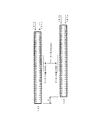
主制御用集積回路130の端子131及び入出力用集積回路140の端子141の配設状態の1例を図4に示す。
主制御用集積回路130には、端子131によって2列の端子列131a(端子番号1〜32)及び131b(端子番号33〜64)が形成されている。また、入出力用集積回路140には、端子141によって2列の端子列141a(端子番号1〜32)及び141b(端子番号33〜64)が形成されている。
本実施の形態では、図4に示すように、主制御用集積回路130では、入出力用集積回路140側に配置されている端子列131aに、データを入出力するデータバス端子DBc(端子番号10〜17の端子の組)を設けている。また、入出力用集積回路140と反対側に配置されている端子列131bに、セレクトデータを出力するセレクト端子Sc(端子番号37〜44の端子の組)を設けている。
一方、入出力用集積回路140では、主制御用集積回路130側に配置される端子列141bに、データを入出力するデータバス端子DBi(端子番号42〜49の端子の組)を設けている。また、主制御用集積回路130と反対側に配置されている端子列141aに、セレクトデータを入力するセレクト端子Si(端子番号1〜8の端子の組)と、主制御基板120に配置されている他の電気回路との間でデータを入出力する複数のデータ端子D1(端子番号9〜16の端子の組)及びD2(端子番号17〜24の端子の組)を設けている。
なお、図4では、2つのデータ端子D1とD2のみを示したが、データ端子の数は主制御回路との間でデータを入出力する外部機器(主制御基板120に配置されている他の電気回路を含む)の数に応じて適宜変更される。
また、セレクト端子Sc及びSiを構成する端子の数は、セレクト信号の形態に応じて適宜設定される。例えば、セレクト端子を構成する各端子によってデータ端子を選択する場合(例えば、端子37から「H」レベルの信号を出力することによってデータ端子D1を選択する場合)には、セレクト端子は、入出力用集積回路140に設けられているデータ端子の数に等しい数の端子により構成される。あるいは、複数ビットの信号によってセレクト信号を構成する場合には、セレクト端子は、ビット数に対応する数の端子により構成される。例えば、8ビットのセレクト信号を用いる場合には、セレクト端子は、8つの端子により構成される。
An example of the arrangement state of the
In the main control integrated
In the present embodiment, as shown in FIG. 4, in the main control integrated
On the other hand, in the input / output integrated
In FIG. 4, only two data terminals D1 and D2 are shown, but the number of data terminals is an external device that inputs / outputs data to / from the main control circuit (other devices arranged on the main control board 120). The number is appropriately changed according to the number of electrical circuits).
The number of terminals constituting the select terminals Sc and Si is appropriately set according to the form of the select signal. For example, when the data terminal is selected by each terminal constituting the select terminal (for example, when the data terminal D1 is selected by outputting a signal of “H” level from the terminal 37), the select terminal is input / output The number of terminals is equal to the number of data terminals provided in the
主制御用集積回路130のデータバス端子DBcが挿入(接続)される制御用挿入部(制御用接続端子)120CPUと、入出力用集積回路140のデータバス端子DBiが挿入(接続)される入出力用挿入部(入出力用接続端子)120IOは、データバス(基板面120aに配設されている配線パターン)DBLによって接続されている。
このように、主制御用集積回路130の、入出力用集積回路140側の端子列120CPUaに含まれている端子をデータバス端子とし、入出力用集積回路140の、主制御用集積回路130側の端子列120IObに含まれている端子をデータバス端子として用いることにより、主制御用集積回路130と入出力用集積回路140との間に配設されるデータバスの長さを短くすることができる。
さらに、本実施の形態では、主制御用集積回路130のデータバス端子DBcと入出力用集積回路140のデータバス端子DBiの配設位置を、主制御用集積回路130と入出力用集積回路140が主制御基板120の基板面120aに配置された時に、データバス端子DBcとDBiが対向するように設定されている。
すなわち、主制御用集積回路130のデータバス端子DBcが挿入(接続)される制御用挿入部120CPUと、入出力用集積回路140のデータバス端子DBiが挿入(接続)される入出力用挿入部120IOを接続するデータバスDBLが、制御用挿入部120CPUと入出力用挿入部120IOの平行方向(主制御用集積回路130と入出力用集積回路140の平行方向)に直角(略直角を含む)な直線状(略直線状を含む)に配設可能に設定されている。
これにより、主制御用集積回路130と入出力用集積回路140との間に配設されるデータバスの長さをより短くすることができる。
The control insertion portion (control connection terminal) 120CPU into which the data bus terminal DBc of the main control integrated
Thus, the terminals included in the terminal row 120CPUa on the input / output integrated
Further, in the present embodiment, the arrangement positions of the data bus terminal DBc of the main control integrated
That is, the control insertion unit 120CPU into which the data bus terminal DBc of the main control integrated
Thereby, the length of the data bus arranged between the main control integrated
また、主制御用集積回路130のセレクト端子Scが挿入(接続)される制御用挿入部120CPUと、入出力用集積回路140のセレクト端子Siが挿入(接続)される入出力用挿入部120IOは、セレクト線(基板面120aに配設された配線パターン)SLによって接続されている。
また、入出力用集積回路140のデータ端子D1及びD2が挿入(接続)される入出力用挿入部120IOと、他の電気回路の端子は、対応するデータ線(基板面120aに配設された配線パターン)DL1及びDL2によって接続されている。
The control insertion portion 120CPU into which the select terminal Sc of the main control integrated
The input / output insertion portion 120IO into which the data terminals D1 and D2 of the input / output integrated
主制御用集積回路130及び入出力用集積回路140は、以下のように動作する。
例えば、主制御用集積回路130に内蔵されている主制御回路から、データ線DL1にデータを出力する場合には、主制御回路は、データバス端子DBcを介してデータバスDBLにデータを出力するとともに、セレクト端子Scにデータ端子D1を示すセレクト信号を出力する。入出力用集積回路140に内蔵されている入出力処理回路は、セレクト端子Siに、データ端子D1を示すセレクト信号が入力されると、データバス端子DBiとデータ端子D1を接続し、データバスDBL上のデータを、データバス端子DBi及びデータ端子D1を介してデータ線DL1に出力する。
また、データ線DL2から主制御回路にデータを入力する場合には、主制御回路は、セレクト端子Scにデータ端子D2を示すセレクト信号を出力する。入出力用集積回路140に内蔵されている入出力処理回路は、セレクト端子Siに、データ端子D2を示すセレクト信号が入力されると、データ端子D2とデータバス端子DBiを接続し、データ線DL2上のデータを、データ端子D2及びデータバス端子DBiを介してデータバスDBLに出力する。主制御回路は、データバスDBLからデータバス端子DBcに入力されたデータを読み取る。
The main control integrated
For example, when data is output from the main control circuit incorporated in the main control integrated
When data is input from the data line DL2 to the main control circuit, the main control circuit outputs a select signal indicating the data terminal D2 to the select terminal Sc. The input / output processing circuit built in the input / output integrated
ところで、パチンコ機等の遊技機では、主制御回路を内蔵する主制御用集積回路130に識別情報を表示することが要求されている。
識別情報としては、図1に示すように、主制御用集積回路130の外周面(例えば、側面)に印刷等によって表示されている識別情報(図1では、「AB−01」)132、制御用集積回路130の外周面(例えば、側面)に貼付されたシール133に印刷等によって表示されている識別情報(図1では、「abcd」)133aが用いられる。
識別情報132としては、主制御用集積回路130(あるいは、主制御用集積回路130に内蔵されている主制御回路)の製造会社名や型番等が用いられ、識別情報133aとしては、主制御用集積回路130が設けられている遊技機の製造会社や機種名や機種番号等が用いられる。
通常、図1及び図3に示すように、主制御用集積回路130の、入出力用集積回路140に対向する側の面(側面130a)に、識別情報132が印刷されるとともに、識別情報133aが印刷されたシール133が貼付される。
このため、主制御用集積回路130に表示されている識別情報(132や133a)を確認することによって、主制御用集積回路130が不正な制御用集積回路に交換されていることを発見することができる。例えば、外観は正規の主制御用集積回路の外観に似せているが、正規の識別情報が表示されていないことを視認(確認)することによって、主制御用集積回路が不正な制御用集積回路に交換されていることを発見することができる。
主制御用集積回路130の外観や制御用集積回路130に表示されている識別情報の視認(確認)は、主制御基板120がケース110に収容されている状態で、ケース110の外部から行われる。
By the way, in gaming machines such as pachinko machines, it is required to display identification information on the main control integrated
As the identification information, as shown in FIG. 1, the identification information (“AB-01” in FIG. 1) 132 displayed on the outer peripheral surface (for example, the side surface) of the main control integrated
As the
Normally, as shown in FIGS. 1 and 3,
Therefore, by confirming the identification information (132 or 133a) displayed on the main control integrated
The appearance (confirmation) of the external appearance of the main control integrated
ここで、ZIP型(縦型)の主制御用集積回路130と入出力用集積回路140を、平行に接近させて主制御基板120の基板面120aに配置した場合、入出力用集積回路140によって、主制御用集積回路130の、入出力用集積回路140に対向する側の面(側面130a)に表示されている識別情報(132や133a)をケース110の外部から視認するのが困難となる。すなわち、主制御用集積回路が不正な制御用集積回路に交換されたことを発見するのが困難となる。
そこで、本実施の形態では、主制御用集積回路130と入出力用集積回路140を、主制御用集積回路130と入出力用集積回路140との間に配設される接続線の抵抗による影響や接続線へのノイズの侵入による影響よりも、不正な制御用集積回路の発見の容易性(不正防止効果の向上)を優先している。
すなわち、主制御用集積回路130と入出力用集積回路140の間の距離Hを、ケース110が遊技機に取り付けられている状態で、主制御用集積回路130の、入出力用集積回路140に対向する側の面(側面130a)に表示されている識別情報(132や133a)を、ケース110の外部から視認可能となる距離に設定している。
Here, when the ZIP type (vertical type) main control integrated
Therefore, in this embodiment, the main control integrated
That is, the distance H between the main control integrated
「識別情報(132や133a)をケース110の外部から視認可能となる距離」として、係員等が、ケース110が遊技機に取り付けられている状態で、ケース110の外部から、通常の視認姿勢で、制御用集積回路130の側面130aに表示されている識別情報(132や133a)全体を視認可能な距離に設定することにより、不正な制御用集積回路を容易に発見することができる。
しかしながら、接続線の抵抗による影響や接続線へのノイズの侵入による影響を軽減し、また、制御基板120の実装効率を高めるためには、主制御用集積回路130と入出力用集積回路140の間の距離は短い方がよい。また、主制御用集積回路130に表示されている識別情報は、その一部を視認することができれば識別情報全体を推定することができる。
したがって、主制御用集積回路130と入出力用集積回路140の間の距離は、係員等が、ケース110が遊技機に取り付けられている状態で、ケース110の外部から、通常の視認姿勢で、制御用集積回路130の側面130aに表示されている識別情を視認した時に識別情報の一部を視認可能であり、且つ、視認した識別情報の一部に基づいて識別情報全体を推定可能な距離以上の距離に設定するのが好ましい。
このような距離に設定することにより、接続線の長さが長くなるのをできる限り抑制しながら、不正防止効果を高めることができる。
識別情報を視認可能な距離(識別情報全体を視認可能な距離あるいは識別情報全体を推定可能な一部の識別情報を視認可能な距離)は、ケース110が遊技機に取り付けられている位置や、ケース110の配設状態等によって異なる。
“Distance where the identification information (132 or 133a) can be visually recognized from the outside of the case 110” indicates that an attendant or the like is in a normal viewing posture from the outside of the case 110 while the case 110 is attached to the gaming machine. By setting the entire identification information (132 or 133a) displayed on the side surface 130a of the control integrated
However, in order to reduce the influence of the resistance of the connection line and the influence of noise intrusion on the connection line, and to improve the mounting efficiency of the
Therefore, the distance between the main control integrated
By setting such a distance, the fraud prevention effect can be enhanced while suppressing the length of the connection line from being increased as much as possible.
The distance at which the identification information can be visually recognized (the distance at which the entire identification information can be viewed or the distance at which a part of the identification information can be estimated) can be determined by the position where the case 110 is attached to the gaming machine, It differs depending on the arrangement state of the case 110 and the like.
主制御用集積回路130に表示されている識別情報を視認可能な、主制御用集積回路130と入出力用集積回路140の距離は、例えば、横型の集積回路として形成された主制御用集積回路(横型の主制御用集積回路)を用いた場合の、基板上の実装面積に基づいて決定することができる。
すなわち、本実施の形態で用いているZIP型(縦型)の主制御用集積回路130と同じ数の端子(64ピン)を有するDIP型(横型)の主制御用集積回路を主制御基板120に配置した場合の、主制御基板120上の実装面積(具体的には、横型の主制御用集積回路に取り付けられている端子の外周を覆う面積)に等しい領域を、ZIP型(縦型)の主制御用集積回路130の周囲に確保することができるように、主制御用集積回路130と入出力用集積回路140の距離を設定する。この領域には、配線パターン以外は配置されない。
通常、横型の主制御用集積回路を、実装面積の小さい縦型の主制御用集積回路に置き換えた場合には、縦型の主制御用集積回路を用いることによる効果を最大限に利用するために(すなわち、接続線を短くするとともに実装効率を高めるために)、縦型の主制御用集積回路の周囲には、横型の主制御用集積回路を主制御基板に配置した場合の実装面積より小さい領域しか確保されない。すなわち、主制御用集積回路と隣接する回路の間の距離は、できるだけ短い値に設定される。
本実施の形態では、接続線の長さが長くなり、また、実装効率が低下するのを許容し、不正防止効果を高めることを優先するため、縦型の主制御用集積回路を用いてはいるが、縦型の主制御用集積回路の周囲には、横型の主制御用集積回路を主制御基板に配置した場合の実装面積に等しい領域を確保している。
なお、「縦型の主制御用集積回路の周囲に、横型の主制御用集積回路を主制御基板に配置した場合の実装面積に等しい領域を確保する」方法としては、例えば、横型の主制御用集積回路と入出力用集積回路を平行に主制御基板上に配置した場合に、横型の主制御用集積回路が配置される領域(実装領域)の中央部に、縦型の主制御用集積回路の端子の配列方向が横型の主制御用集積回路の端子の配列方向と同じ方向となるように、縦型の主制御用集積回路を主制御基板に配置する。
主制御用集積回路130と入出力用集積回路140の間の距離をこのように設定することにより、主制御用集積回路130の入出力用集積回路140側の面に表示されている識別情報の視認が可能となるように、制御用集積回路と入出力用集積回路を容易に配置することができる。
The distance between the main control integrated
That is, the
Normally, when the horizontal main control integrated circuit is replaced with a vertical main control integrated circuit with a small mounting area, the effect of using the vertical main control integrated circuit is maximized. (I.e., to shorten the connection line and increase the mounting efficiency), the area around the vertical main control integrated circuit is larger than the mounting area when the horizontal main control integrated circuit is arranged on the main control board. Only a small area is reserved. That is, the distance between the main control integrated circuit and the adjacent circuit is set to a value as short as possible.
In this embodiment, the length of the connection line is increased, and it is allowed to reduce the mounting efficiency, and priority is given to enhancing the fraud prevention effect. Therefore, the vertical main control integrated circuit is used. However, an area equal to the mounting area when the horizontal main control integrated circuit is arranged on the main control board is secured around the vertical main control integrated circuit.
In addition, as a method of “securing a region equal to the mounting area when the horizontal main control integrated circuit is arranged on the main control board around the vertical main control integrated circuit”, for example, the horizontal main control When the integrated circuit for input and the integrated circuit for input / output are arranged in parallel on the main control board, the vertical main control integrated circuit is arranged at the center of the area (mounting area) where the horizontal main control integrated circuit is arranged. The vertical main control integrated circuit is arranged on the main control board so that the arrangement direction of the circuit terminals is the same as the arrangement direction of the terminals of the horizontal main control integrated circuit.
By setting the distance between the main control integrated
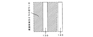
「縦型の主制御用集積回路の周囲に、横型の主制御用集積回路を主制御基板に配置した場合の実装面積に等しい領域を確保可能な距離だけ離して主制御用集積回路130と入出力用集積回路140を主制御基板120に配置する」例を図5〜図7に示す。
図5は、主制御用集積回路130に対する不正防止効果の向上を目的とした配置例であり、図6及び図7は、主制御用集積回路130及び入出力用集積回路140に対する不正防止効果の向上を目的とした配置例である。
図5では、ZIP型の主制御用集積回路130と同じ端子の数(64ピン)を有するDIPの主制御用集積回路を主制御基板120に配置した場合の実装領域(左下がりのハッチングで示す領域)の中央部に、ZIP型の主制御用集積回路130を、ZIP型の主制御用集積回路130の端子の配列方向が、DIP型の主制御用集積回路の端子の配列方向と同じ方向(図5では、長方形の実装領域の長辺方向である上下方向)となるように配置している。そして、ZIP型の主制御用集積回路130の周囲に、DIP型の主制御用集積回路の実装領域を確保した状態で、入出力用集積回路140を配置している。DIP型の主制御用集積回路の実装領域内には、配線パターン以外の構成要素は配置されていない。
これにより、主制御用集積回路130の入出力用集積回路140側の面に表示されている識別情報の視認が可能となる。また、主制御用集積回路130の周囲に不正な回路が配設されていることを容易に発見することができる。
なお、主制御用集積回路130と入出力用集積回路140の間の距離は、図5に示す距離以上であればよい。
“The main control integrated
FIG. 5 is an example of an arrangement intended to improve the fraud prevention effect on the main control integrated
In FIG. 5, a mounting area (indicated by hatching at the lower left) when a DIP main control integrated circuit having the same number of terminals (64 pins) as the ZIP type main control integrated
This makes it possible to visually recognize the identification information displayed on the surface of the main control integrated
Note that the distance between the main control integrated
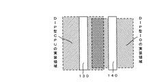
図6では、主制御用集積回路130と同様に、ZIP型の入出力用集積回路140と同じ端子の数(64ピン)を有するDIP型の入出力用集積回路を主制御基板120に配置した場合の実装領域(右下がりのハッチングで示す領域)の中央部に、ZIP型の入出力用集積回路140を、ZIP型の入出力用集積回路140の端子の配列方向が、DIP型の入出力用集積回路の端子の配列方向と同じ方向(図6では、長方形の実装領域の長辺方向である上下方向)となるように配置している。図6では、主制御用集積回路130の、入出力用集積回路140側の周囲に確保する領域と、入出力用集積回路140の、主制御用集積回路130側の周囲に確保する領域を重複させている。
図6では、DIP型の主制御用集積回路の実装領域及びDIP型の入出力用集積回路の実装領域内には、配線パターン以外の構成要素は配置されていない。
これにより、主制御用集積回路130の入出力用集積回路140側の面に表示されている識別情報の視認や入出力用集積回路140の主制御用集積回路130側の面に表示されている識別情報の確認が可能となる。また、主制御用集積回路130の周囲や入出力用集積回路140の周囲に不正な回路が配設されていることを容易に発見することができる。
通常、64ピン構造のDIP型の主制御用集積回路と入出力用集積回路の実装面積はほぼ等しく、また、64ピン構造の縦型の主制御用集積回路と入出力用集積回路の実装面積はほぼ等しい。このため、図6に示すように、主制御用集積回路130の、入出力用集積回路140側の周囲に確保する領域と、入出力用集積回路140の、主制御用集積回路130側の周囲に確保する領域をほぼ100%重複させることができる。この場合、主制御用集積回路130と入出力用集積回路140の間の距離を短くすることができ、主制御基板120の実装効率を高めることができ。
なお、主制御用集積回路130と入出力用集積回路140の間の距離は、図6に示す距離以上であればよい。
In FIG. 6, like the main control integrated
In FIG. 6, no components other than the wiring pattern are arranged in the mounting area of the DIP type main control integrated circuit and the mounting area of the DIP type input / output integrated circuit.
As a result, the identification information displayed on the surface on the input / output integrated
Usually, the mounting area of the 64-pin structure DIP main control integrated circuit and the input / output integrated circuit are substantially equal, and the mounting area of the 64-pin vertical main control integrated circuit and the input / output integrated circuit. Are almost equal. Therefore, as shown in FIG. 6, a region to be secured around the input / output integrated
Note that the distance between the main control integrated
また、主制御用集積回路130と入出力用集積回路140の間に配置されるデータバスにプルアップ用あるいはプルダウン用の抵抗アレイを配置する必要がある場合がある。
この場合、不正防止効果の向上に対する要求が高い主制御用集積回路130の周囲に確保する領域内には抵抗アレイを配置しない。すなわち、図7に示すように、主制御用集積回路130の領域(左下がりのハッチングで示す、横型の主制御用集積回路の実装領域)より入出力用集積回路140側に、少なくとも抵抗アレイ125を配置するのに必要な距離Wだけ重ならない状態で、入出力用集積回路140の領域(右下がりのハッチングで示す、横型の入出力用集積回路の実装領域)が確保されるように、主制御用集積回路130と入出力用集積回路140の間の距離を設定する。
なお、主制御用集積回路130と入出力用集積回路140の間の距離は、図7に示す距離以上であればよい。
また、主制御用集積回路130の領域と入出力用集積回路140の領域が、抵抗アレイ125を配置するのに必要な距離Wだけ離れた位置に配置されるように、主制御用集積回路130と入出力用集積回路140の間の距離を設定することもできる。
Further, it may be necessary to arrange a pull-up or pull-down resistor array on a data bus arranged between the main control integrated
In this case, the resistor array is not arranged in a region secured around the main control integrated
Note that the distance between the main control integrated
In addition, the main control integrated
また、縦型の主制御用集積回路130と入出力用集積回路140を平行に近接して配置した場合、主制御用集積回路130と入出力用集積回路140が壁となり、主制御用集積回路130と入出力用集積回路140の間に不正回路が配設されていることを発見するのが困難である。
本実施の形態では、主制御用集積回路130と入出力用集積回路130の間の距離を、主制御用集積回路130の入出力用集積回路140側の面に表示されている識別情報を視認可能な距離に設定することにより、不正な主制御用集積回路が配設されていることを容易に発見することができるとともに、平行に配置された縦型の主制御用集積回路130と入出力用集積回路140の間に不正な回路が配設されたことも容易に発見することができる。
Further, when the vertical main control integrated
In the present embodiment, the distance between the main control integrated
主制御基板120には、主制御用集積回路130に内蔵されている主制御回路の動作用のクロック信号を発生する発振器122が配置されている。
ここで、主制御用集積回路130と入出力用集積回路140の間に配設されているデータバスDBLには多くの入出力信号が流れるため、データバスDBLにノイズが侵入すると主制御回路や外部機器が誤動作する恐れがある。
そこで、本実施の形態では、発振器122から発生するノイズがデータバスDBLに侵入するのを防止するように発振器122を配置している。
すなわち、図2に示すように、発振器122を、主制御用集積回路130を挟んで入出力用集積回路140と反対側に配置している。また、主制御用集積回路130の、入出力用集積回路140と対抗する側と反対側の端子列131bにクロック端子CLc(端子番号56〜59の端子の組)を設けている。そして、発振器122とクロック端子CLcを、クロック線(配線パターン)CLによって接続している。
このように、発振器122とデータバスDLBを離して配置しているため、発振器122から発生するノイズがデータバスDBLに侵入するのを防止することができ、データバスDBLを流れるデータにノイズが混入するのを防止することができる。
なお、発振器122の端子とクロック端子CLcが対向するように、発振器122の配置位置あるいはクロック端子CLcの配設位置を設定するのが好ましい。これにより、クロック線CLの長さを短くすることができる。
On the
Here, since many input / output signals flow through the data bus DBL disposed between the main control integrated
Therefore, in this embodiment, the
That is, as shown in FIG. 2, the
As described above, since the
Note that it is preferable to set the position of the
また、主制御基板120には、外部機器から出力されるデータを入出力用集積回路140のデータ端子に入力し、あるいは、入出力用集積回路140のデータ端子から出力されるデータを外部機器に出力するために、外部機器に接続された接続端子を有するプラグ(接続部材)が挿入可能なソケット121が配置されている。図1及び図2では、ソケット121が1つしか記載されていないが、通常、ソケット121は複数設けられる。
本実施の形態では、ソケット121を、入出力用集積回路140を挟んで主制御用集積回路130と反対側に配置している。これにより、入出力用集積回路140のデータ端子とソケット121に設けられている接続端子との間のデータ線の長さを短くすることができる。
また、ソケット121の接続端子の配列方向が入出力用挿入部列120IOa及び120IObの配列方向と平行になるように、すなわち、ソケット121と入出力用集積回路140が平行に配置されるように、ソケット121が主制御基板120に配置されている。これにより、入出力用集積回路140のデータ端子が挿入(接続)される入出力挿入部120IOとソケット121の接続端子の間、したがって、入出力用集積回路140のデータ端子とソケット121の接続端子の間のデータ線の長さを短くすることができる。
なお、ソケット121と入出力用集積回路140が主制御基板120に配置された状態で、ソケット121の接続端子と、入出力用集積回路140のデータ端子が挿入(接続)される入出力挿入部120IO(入出力用挿入部列141aの入出力用挿入部)が対向するようにソケット121の配置位置あるいは入出力用集積回路140における入出力用挿入部の配設位置を設定することにより、出力用集積回路140のデータ端子とソケット121の接続端子の間のデータ線の長さをさらに短くすることができる。
Further, the
In the present embodiment, the socket 121 is disposed on the opposite side of the main control integrated
Further, the arrangement direction of the connection terminals of the socket 121 is parallel to the arrangement direction of the input / output insertion row 120IOa and 120IOb, that is, the socket 121 and the input / output integrated
The input / output insertion section into which the connection terminal of the socket 121 and the data terminal of the input / output integrated
ところで、パチンコ機では、主制御用集積回路に対する不正だけでなく、主制御回路に入力される入力データに対する不正、例えば、不正な入力信号を出力可能な不正回路を設ける不正が行われことがある。
このため、入出力用集積回路140とソケット121の間の距離Kを長くして、入出力用集積回路140とソケット121との間の領域に不正な入力信号を出力する不正回路が設けられていることを容易に発見できるようにするのが好ましい。本実施の形態では、入出力用集積回路140とソケット121の間の距離Kを、主制御用集積回路130と入出力用集積回路140との間の距離Hより大きい距離に設定している。
ソケット121には、入出力用集積回路140のデータ端子D1やD2に接続されているデータ線DL1やDL2が接続される接続端子が設けられている。また、ケース110の、ソケット121に対応する箇所に孔111が設けられている。孔111にプラグ(接続部材)を挿入することによって、プラグの端子がソケットの接続端子に接続される。
なお、ソケット121の接続端子がデータ端子と対向するようにソケット121の配置位置あるいはデータ端子の配設位置を設定するのが好ましい。
この場合には、不正な回路の発見の容易性を高める(不正防止効果を高める)ために入出力用集積回路140とソケット121を離して配置することにより、入出力用集積回路140のデータ端子とソケット121の接続端子の間に配設されるデータ線の長さが長くなるのを抑制することができる。
By the way, in the pachinko machine, not only illegality with respect to the main control integrated circuit but also illegality with respect to input data input to the main control circuit, for example, illegality with an illegal circuit capable of outputting an illegal input signal may be performed. .
For this reason, an illegal circuit that increases the distance K between the input / output integrated
The socket 121 is provided with a connection terminal to which the data lines DL1 and DL2 connected to the data terminals D1 and D2 of the input / output integrated
Note that it is preferable to set the position of the socket 121 or the position of the data terminal so that the connection terminal of the socket 121 faces the data terminal.
In this case, the input / output integrated
主制御用集積回路130や入出力用集積回路140から(詳しくは、主制御用集積回路130や入出力用集積回路140に内蔵されている構成要素から)ノイズが発生する場合がある。主制御用集積回路130や入出力用集積回路140から発生したノイズが外部に放出されると、外部機器(主制御基板120に配置されている電気回路を含む)が誤動作する恐れがある。
本実施の形態では、主制御用集積回路130や入出力用集積回路140から発生したノイズが外部に放出されるのを防止するために、主制御用集積回路130や入出力用集積回路140の下方の基板面に接地線を配設している。
主制御用集積回路130の下方に接地線を配設する構成を、図8〜図10を用いて説明する。なお、図9は、図8のIX線矢視図(平面図)であり、図10は、図9のX−X線断面図である。
Noise may be generated from the main control integrated
In this embodiment, in order to prevent noise generated from the main control integrated
A configuration in which a ground line is disposed below the main control integrated
前述したように、ZIP型(縦型)の主制御用集積回路130の、基板面120aと対向する面(底面)130cには、端子131が長辺方向にジグザグ状に交互に配列されている。これにより、端子131の先端部によって、2列の端子列131a及び131bが形成されている。また、主制御基板120には、主制御用集積回路130の端子131が挿入可能(接続可能)な主制御用挿入部120CPUが設けられている。制御用挿入部120CPUは、主制御用集積回路130の2列の端子列131a及び131bに対応する2列の主制御用挿入部列120CPUa及び120CPUbを有している。これにより、主制御用集積回130が主制御基板120に配置された状態では、最も大きい面積を有する面(図10では、側面130a、130b)が主制御基板120の基板面(実装側基板面)120aから立ち上がるように配置される。
As described above, on the surface (bottom surface) 130c facing the substrate surface 120a of the ZIP type (vertical) main control integrated
また、主制御基板120の基板面120a(実装側基板面)及び基板面120b(反実装側基板面)の、主制御用集積回路130の底面130cに対向する箇所に接地線120Gf及び120Gbが配設されている。
すなわち、図10に示すように、主制御基板120には、基板面120aと120bを貫通し、主制御用集積回路130の端子131により形成される2列の端子列131a及び131bに対応する2列の主制御用挿入部列120CPUa及び120CPUbを形成する主制御用挿入部120CPUが設けられている。
そして、基板面120a及び120bには、2列の主制御用挿入部列120CPUaと120CPUbの間に、主制御用挿入部列120CPUa及び120CPUbの配列方向に沿って接地線120Gf及び120Gbが直線状に配設されている。
本実施の形態では、接地線120Gf及び120Gbとして、主制御基板120の基板面120a及び120bに配設され、主制御基板120の接地端子に接続されている配線パターンを用いている。なお、主制御用集積回路130の端子131には接地端子が含まれており、この接地端子は、接地線120Gf及び120Gbに接続される。
接地線120Gf及び120Gbの配設位置は、2列の主制御用挿入部列120CPUaと120CPUbの間の中央部が好ましいが、2列の制御用挿入部列120CPUaと120CPUbの間であればよい。また、接地線120Gf及び120Gbは直線状でなくてもよい。
本実施の形態では、入出力用集積回路140に対しても同様の接地線120Hf及び120(図示省略)を設けている。
なお、接地線は、主制御用集積回路130あるいは入出力用集積回路140のいずれか一方に対してのみ設けてもよい。また、主制御基板120の基板面120a(実装側基板面)あるいは基板面120b(半実装側基板面)の一方側のみに設けてもよい。この場合でも、回路から発生するノイズが外部に放出するのを防止することができる。
In addition, the ground lines 120Gf and 120Gb are arranged at locations on the substrate surface 120a (mounting side substrate surface) and the substrate surface 120b (non-mounting side substrate surface) of the
That is, as shown in FIG. 10, the
On the board surfaces 120a and 120b, the ground lines 120Gf and 120Gb are linearly arranged between the two main control insertion row 120CPUa and 120CPUb along the arrangement direction of the main control insertion row 120CPUa and 120CPUb. It is arranged.
In the present embodiment, as the ground lines 120Gf and 120Gb, wiring patterns disposed on the board surfaces 120a and 120b of the
The arrangement position of the ground lines 120Gf and 120Gb is preferably in the center between the two rows of main control insertion rows 120CPUa and 120CPUb, but may be between the two rows of control insertion rows 120CPUa and 120CPUb. Further, the ground lines 120Gf and 120Gb may not be linear.
In the present embodiment, similar ground lines 120Hf and 120 (not shown) are also provided for the input / output integrated
The ground line may be provided only for either the main control integrated
なお、主制御用集積回路130の端子列131aと131bの間(すなわち、制御用挿入部列120CPUaと120CPUbの間)あるいは入出力用集積回路140の端子列141aと14bの間(すなわち、入出力用挿入部列120IOaと120iobの間)に不正な回路が配設される場合がある。
本実施の形態では、主制御基板120の基板面120aの、主制御用集積回路130の端子列131aと131bの間あるいは入出力用集積回路140の端子列141aと14bの間に接地線120Gf、120Hfが配設されている。
このため、主制御用集積回路130の端子列131aと131bの間あるいは入出力用集積回路140の端子列141aと14bの間に不正な回路が配設されるのを防止することができる。また、不正な回路が配設された場合でも、不正な回路が配設されたことを容易に発見することができる。
Note that, between the
In the present embodiment, a ground line 120Gf between the
Therefore, it is possible to prevent an unauthorized circuit from being arranged between the
本実施の形態では、主制御用集積回路130と外部機器(主制御基板に配置されている他の電気回路を含む)との間に入出力用集積回路140を設けているため、主制御用集積回路130と外部機器との接続状態の変更や外部機器の数の増減に対して安価に容易に対応することができ、主制御用集積回路130の汎用性を高めることができる。
また、主制御用集積回路130と入出力用集積回路140として縦型(ZIP型)の集積回路を用いているため、主制御用集積回路130や入出力用集積回路140が不正な制御用集積回路や不正な入出力用集積回路に交換されたこと、主制御用集積回路や入出力用集積回路と主制御基板との間に不正な回路が設けられていることを容易に発見することができ、不正防止効果を高めることができる。同時に、主制御用集積回路130と入出力用集積回路140の主制御基板120上での実装面積を低減することができるため、主制御基板120の実装効率を高めることができる。
さらに、縦型(ZIP型)の主制御用集積回路130と入出力用集積回路140を、主制御用集積回路130の、入出力用集積回路140と対向する側の面に表示されている識別情報を、主制御基板120を収容したケース110を遊技機に取り付けた状態で、ケース110の外部から視認可能となるように離して平行に主制御基板120に配置しているため、主制御用集積回路130と入出力用集積回路140の間に配設されるデータバスの長さが長くなる量を最小限に抑えながら、外観を正規の主制御用集積回路に似せているが正規の識別情報が表示されていない不正な制御用集積回路が設けられていることを容易に発見することができる。これにより、主制御用集積回路130と入出力用集積回路との間に配設されるデータバスの抵抗による影響やデータバスへのノイズの侵入を最小限に抑えながら、不正防止効果をより高めることができる。さらに、主制御用集積回路130と入出力用集積回路140の間に不正な回路が設けられたことを容易に発見することができる。
また、入出力用集積回路140を主制御用集積回路130より、主制御基板120の基板面120aの中心部側に配置しているため、入出力用集積回路140と他の電気回路の間に配設される接続線を短くすることができる。
また、主制御用集積回路130、入出力用集積回路140、ソケット121を、主制御基板120の長方形の基板面120aの長辺方向に沿って(長辺に平行に)配置しているため、主制御基板120の実装効率を高めることができる。
また、外部機器と接続されるソケット121を、入出力用集積回路140を挟んで主制御用集積回路130と反対側に、主制御用集積回路130と入出力用集積回路140との間の距離より長い距離だけ離して入出力用集積回路140に平行に配置しているため、入出力用集積回路140とソケット121の間に不正な回路が設けられたことを容易に発見することができ、不正防止効果を高めることができる。
また、主制御回路の動作用クロック信号を出力する発振器122を、主制御用集積回路130を挟んで入出力用集積回路140と反対側に配置しているため、発振器122から発生するノイズが、主制御回路用集積回路130と入出力用集積回路140の間に配設されるデータバスに侵入するのを防止することができる。
また、主制御用集積回路130及び入出力用集積回路140の少なくとも一方の、主制御基板120に対向する面(底面130c)に対向する主制御基板120の箇所には、主制御基板120の基板面120a及び120bの少なくとも一方に接地線120Gf及び120Gbが配設されているため、主制御用集積回路130や入出力用集積回路140から発生するノイズが接地線120a及び120bに流れる。これにより、主制御用集積回路130や入出力用集積回路140から発生するノイズの外部への放出を防止することができ、外部機器(主制御基板120に配置されている他の電気回路を含む)の誤動作等を防止することができる。さらに、主制御用集積回路130の端子列の間あるいは入出力用集積回路140の端子列の間に不正な回路が設けられるのを防止することができる。
なお、本実施の形態は、主制御用集積回路130と入出力用集積回路140が、縦型の集積回路として形成され、主制御用集積回路130の、入出力用集積回路140と対向する面に表示されている識別情報をケース110の外部から視認可能に平行に離して配置されている構成を備えていればよく、他の構成要素は適宜選択可能である。勿論、他の構成要素を付加することによって、種々の効果を得ることができる。
In this embodiment, since the input / output integrated
Further, since a vertical (ZIP type) integrated circuit is used as the main control integrated
Further, the vertical (ZIP type) main control integrated
Further, since the input / output integrated
In addition, since the main control integrated
The distance between the main control integrated
In addition, since the
Further, at least one of the main control integrated
In this embodiment, the main control integrated
以上の実施の形態では、主制御用集積回路130の、入出力用制御基板140に対向する側の端子列131aにおけるデータバス端子DBcと、入出力用集積回路140の、主制御用集積回路130に対向する側の端子列141bにおけるデータバス端子DBiの長辺方向の配設位置が略同じ場合について説明したが、主制御用集積回路130のデータバス端子DBcの長辺方向の配設位置と、入出力用集積回路140のデータバス端子DBiの長辺方向の配設位置が異なる場合がある。
以下に、このような場合でも、主制御用集積回路130と入出力用集積回路140との間に配設される接続線の長さを長くすることなく、不正防止効果を高めることができる第2の実施の形態を説明する。
第2の実施の形態の要部の斜視図を図11に示し、平面図を図12に示す。
In the above embodiment, the data bus terminal DBc in the terminal row 131 a on the side facing the input /
Hereinafter, even in such a case, the anti-fraud effect can be enhanced without increasing the length of the connection line provided between the main control integrated
The perspective view of the principal part of 2nd Embodiment is shown in FIG. 11, and a top view is shown in FIG.
本実施の形態では、図12に示すように、主制御用集積回路130の、入出力用集積回路140と対向する側の端子列131aにおけるデータバス端子DBc(長辺方向の配設位置)と、入出力用集積回路140の、主制御用集積回路130と対向する側の端子列141bにおけるデータバス端子DBiの配設位置(長辺方向の配設位置)が異なっている。すなわち、主制御用集積回路130では、端子列131aの端子番号15〜22の端子の組がデータバス端子DBcとして設定されている。また、入出力用集積回路140では、端子列141bの端子番号44〜51の端子の組がデータバス端子DBiとして設定されている。
本実施の形態では、図12に示すように、主制御用集積回路130及び入出力用集積回路140が主制御基板120に配置された時に、主制御用集積回路130のデータバス端子DBcと入出力用集積回路140のデータバス端子DBiが対向するように、主制御用集積回路130あるいは入出力用集積回路140の配置位置を平行方向にずらせている。すなわち、前述した実施の形態では、主制御用集積回路130入出力用集積回路140は、平行方向の配置位置が一致(略一致を含む)している(平行方向の両端部の位置が一致している)が、本実施の形態では、平行方向の配置位置がずれている(一方の集積回路の平行方向の一方の端部が、他方の集積回路の平行方向の両端部の間に配置されている)。
例えば、入出力用集積回路140の端子141が挿入(接続)される入出力用挿入部120IOを、主制御用集積回路130の端子131が挿入(接続)される主制御用挿入部120CPUに対して、図11に示す矢印の方向(平行方向)に距離Sだけずらす。平行方向にずらせる量は、データバス端子DBcの長辺方向における配設位置とデータバス端子DBiの長辺方向における配設位置とのずれ量に応じて設定される。
これにより、主制御用集積回路130のデータバス端子DBcと入出力用集積回路140のデータバス端子DBiを接続するデータバス(制御用集積回路130と入出力用集積回路140との間に配設されるデータバス)DBLの長さを短くすることができる。
In the present embodiment, as shown in FIG. 12, the data bus terminal DBc (arrangement position in the long side direction) in the terminal row 131a of the main control integrated
In this embodiment, as shown in FIG. 12, when the main control integrated
For example, the input / output insertion section 120IO into which the terminal 141 of the input / output integrated
As a result, the data bus connecting the data bus terminal DBc of the main control integrated
ところで、主制御用集積回路130と入出力用集積回路140を平行方向にずらせて配置した場合、図11に示すように、主制御用集積回路130の、入出力用集積回路140と対向する側の面(側面130a)に、入出力用集積回路140と対向しない箇所が発生する。すなわち、主制御用集積回路130の側面120aを入出力用集積回路130側から見たとき、入出力用集積回路140と重ならない箇所が発生する。
この場合、主制御用集積回路130の、入出力用集積回路140と対向する側の側面130aの、入出力用集積回路140と対向しない箇所(入出力用集積回路140と重ならない箇所)に表示されている識別情報(図11では、シール133に表示されている識別情報133a)は、ZIP型(縦型)の主制御用集積回路130及び入出力用集積回路140が平行に主制御基板120に配置されていても、主制御基板120を収容したケースI10が遊技機に取り付けられている状態で、ケース110の外部から容易に視認することができる。
したがって、主制御用集積回路130と入出力用集積回路140を平行方向にずらせて配置した場合には、ずらせて配置しない場合に比べて、主制御用集積回路130の側面130aに表示されている情報識別を視認可能な、主制御用集積回路130と入出力用集積回路140との間の距離Hの最小距離を短くすることができる。すなわち、主制御用集積回路130と入出力用集積回路140との間に配設される接続線の長さをより短くすることができる。
When the main control integrated
In this case, the side surface 130a on the side facing the input / output integrated
Therefore, when the main control integrated
なお、主制御用集積回路130の側面130aに表示される識別情報132の表示位置や主制御用集積回路130の側面130aに貼付されるシール133の貼付位置を変更可能である場合には、主制御用集積回路130と入出力用集積回路140を平行方向にずらせて配置した時に、主制御用集積回路130の側面130aの、入出力用集積回路140と対向しない箇所に識別情報132を表示し、あるいは、シール133を貼付する方法を用いてもよい。
この場合、識別情報132あるいはシール133に表示されている識別情報133aの視認結果から識別情報132あるいは133aの全体を推定可能な範囲内において、識別情報132あるいは133aの一部を入出力用集積回路140と対向しない箇所に表示してもよい。
この方法を用いると、主制御用集積回路130と入出力用集積回路140の平行方向のずれ量が変更された場合でも、ずれ量に応じて識別情報132の表示位置やシール133の貼付位置を変更することにより、主制御用集積回路130と入出力用集積回路140を平行方向にずらせて配置しない場合に比べて、主制御用集積回路130と入出力用集積回路140との間の距離を短くしながら、識別情報の視認性を確保することができる。
When the display position of the
In this case, a part of the
When this method is used, even when the shift amount in the parallel direction between the main control integrated
また、前記とは逆に、主制御用集積回路130の、入出力用集積回路140と対向する側の面(側面130a)に表示されている識別情報(132あるいは133a)の少なくとも一部が、入出力用集積回路140と対向しない箇所に配置されるように主制御用集積回路130と入出力用集積回路140を平行方向にずらせ、この状態で対向する位置にある主制御用集積回路130の端子131及び入出力用集積回路140の端子141をデータバス端子として用いるようにすることもできる。「識別情報の少なくとも一部」は、識別情報の一部によって識別情報全体を推定可能な部分を意味する。
また、必ずしも、主制御用集積回路130と入出力用集積回路140を平行方向にずらせて配置した状態で、対向する位置にある主制御用集積回路130の端子131及び入出力用集積回路140の端子141をデータバス端子として用いる必要はない。
このような構成を用いることによっても、平行に配置された縦型の主制御用集積回路130と入出力用集積回路140を用いた場合に、主制御用集積回路130の入出力用集積回路側の面に表示されている識別情報を視認することができ、主制御用集積回路130と入出力用集積回路140との間の距離を短くしながら、識別情報の視認性を確保することができる。
Contrary to the above, at least a part of the identification information (132 or 133a) displayed on the surface (side surface 130a) of the main control integrated
In addition, the main control integrated
Even when such a configuration is used, when the vertical main control integrated
なお、主制御用集積回路130と入出力用集積回路140を平行方向にずらせる技術と第1の実施の形態で用いている各技術のいずれかあるいは複数を組み合わせることもできる。この場合には、主制御用集積回路130の、入出力用集積回路対向する側の面に表示されている識別情報をより容易に、確実に視認することができきる。
Note that a technique for shifting the main control integrated
ところで、前述した実施の形態では、主制御用集積回路130及び入出力用集積回路140として、同じ外形形状を有し、端子の数及び配置形状が同じである集積回路を用いている。このため、主制御用集積回路の端子が挿入(接続)される主制御用挿入部と入出力用集積回路の端子が挿入(接続)される入出力用挿入部が同じ配置形状となり(2列の主制御用挿入部列により形成される主制御用集積回路取付部と2列の入出力用挿入部列により形成される入出力用集積回路取付部が同じ外観となり)、主制御用集積回路130と入出力用集積回路140を間違えて配置する可能性がある。例えば、主制御用集積回路130の端子131を、入出力用集積回路140の端子141が挿入され入出力用挿入部120IOに誤挿入する恐れがある。
このような場合、従来では、作業員は、集積回路に表示されている識別情報(例えば、製造会社名や型番等)を視認することによって、集積回路が主制御用集積回路130であるか入出力用集積回路140であるかを判別し、集積回路の配置位置を判別している。
By the way, in the above-described embodiment, as the main control integrated
In such a case, conventionally, an operator enters whether the integrated circuit is the main control integrated
しかしながら、集積回路に表示されている識別情報を視認する方法は、面倒であり、また、視認ミスが発生する可能性がある。
そこで、以下に、このように同じ外径形状を有している制御用集積回路130と入出力用集積回路の配置位置を確実に判別することができる第3の実施の形態を説明する。
本実施の形態の要部の斜視図を図13に示す。
However, the method of visually recognizing the identification information displayed on the integrated circuit is cumbersome and a visual error may occur.
Therefore, a third embodiment that can reliably determine the arrangement positions of the control integrated
FIG. 13 shows a perspective view of the main part of the present embodiment.
本実施の形態では、前述した実施の形態と同様に、主制御用集積回路130及び入出力用集積回路140として、同じ外形形状を有し、端子131と141の数及び配置形状が同じである、ZIP型(縦型)の集積回路を用いている。すなわち、主制御用集積回路130には、主制御基板120と対向する側の面(底面130c)の長辺方向にジグザグ状に交互に配置された端子131により2列の端子列131a及び131bが形成されている。また、入出力用集積回路140には、主制御基板120と対向する側の面の長辺方向にジグザグ状に交互に配置された端子141により2列の端子列141a及び141bが形成されている。(図14参照)
また、主制御基板120には、主制御用集積回路130の端子131が挿入され、端子列131a及び131bに対応する主制御用挿入部列120CPUa及び120CPUbを有する主制御用挿入部120が設けられているとともに、入出力用集積回路140の端子141が挿入され、端子列141a及び141bに対応する入出力用挿入部列120IOa及び120IObを有する入出力用挿入部120IOが設けられている。(図14参照)
そして、主制御用集積回路130の端子131の配置形状と入出力用集積回路140の端子141の配置形状、したがって、主制御用挿入部120CPUの配置形状と入出力用挿入部120IOの配置形状が同じになるように構成されている。
In this embodiment, as in the above-described embodiment, the main control integrated
Further, the
The arrangement shape of the
本実施の形態では、同じ外形形状を有する主制御用集積回路130と入出力用集積回路140を判別可能とすることによって主制御用集積回路130及び入出力用集積回路140の配置位置を容易に判別可能とするために、図13に示すように、主制御用集積回路130と入出力用集積回路140に異なる色を表示している。
主制御用集積回路130と入出力用集積回路140に表示する色を変える方法としては、全体の色を変える方法や、所定の箇所の色を変える方法等を用いることができる。所定の箇所としては、作業員等が容易に視認することができる箇所、例えば、主制御用集積回路130や入出力用集積回路140の上面(反基板面側の面)を選択するのが好ましい。
また、主制御用集積回路130と入出力用集積回路140の全体あるいは部分の模様を変える方法を用いることができる。模様を変える態様には、一方を無地とし、他方に模様を表示する態様が含まれる。模様は色によって構成されているため、表示する模様を変える方法は、表示する色を変える概念に含まれる。
異なる色や異なる模様としては、作業員等が一瞥して判別可能な色や模様を用いるのが好ましい。
In the present embodiment, the main control integrated
As a method of changing the colors displayed on the main control integrated
Further, a method of changing the pattern of the whole or part of the main control integrated
As the different color or pattern, it is preferable to use a color or pattern that can be discriminated by an operator or the like.
本実施の形態では、同じ外形形状を有する主制御用集積回路130と入出力用集積回路140の色を変えている。
このため、作業員等は、集積回路の色を視認するのみで、集積回路が主制御用集積回路130であるか入出力用集積回路140あるかを簡単に、確実に判別することができる。したがって、端子や挿入部の数や配置状態が同じ場合でも、集積回路の配置位置を間違えることがない。
In the present embodiment, the colors of the main control integrated
Therefore, a worker or the like can easily and surely determine whether the integrated circuit is the main control integrated
以上の実施の形態では、主制御用集積回路と入出力用集積回路に表示する色を変えたが、さらに、主制御基板の基板面の、主制御用挿入部が設けられている近傍及び入出力用挿入部が設けられている近傍に、それぞれ主制御用集積回路及び入出力用集積回路と同じ色を表示してもよい。
以下に、主制御用集積回路及び主制御用挿入部の近傍に表示する色と入出力用集積回路及び入出力用挿入部の近傍に表示する色を変えた第4の実施の形態を説明する。
本実施の形態の要部の斜視図を図14に示す。
In the above embodiment, the colors displayed on the main control integrated circuit and the input / output integrated circuit are changed, but in addition, on the substrate surface of the main control board, in the vicinity of the main control insertion portion and the input. The same color as that of the main control integrated circuit and the input / output integrated circuit may be displayed in the vicinity where the output insertion portion is provided.
A fourth embodiment in which the color displayed in the vicinity of the main control integrated circuit and the main control insertion portion and the color displayed in the vicinity of the input / output integrated circuit and the input / output insertion portion will be described below. .
FIG. 14 shows a perspective view of the main part of the present embodiment.
本実施の形態では、第3の実施の形態と同様に、主制御用集積回路130及び入出力用集積回路140として、同じ外形形状を有するZIP型(縦型)の集積回路を用いている。また、主制御用集積回路130の端子131及び入出力用集積回路140の端子141、主制御用挿入部120CPU及び入出力用挿入部120IOの数及び配置形状は同じである。
また、第3の実施の形態と同様に、主制御用集積回路130及び入出力用集積回路140には、異なる色が表示されている。例えば、主制御用集積回路130及び入出力用集積回路140の全体あるいは一部に異なる色が表示されている。
さらに、主制御基板120の基板面(実装側基板面)120aに設けられている、主制御用集積回路130の端子131が挿入される主制御用挿入部120CPUの近傍に主制御用表示部(CPU用表示部)が表示されているとともに、入出力用集積回路140の端子141が挿入される入出力用挿入部120IOの近傍に入出力用表示部(IO用表示部)が表示されている。本実施の形態では、主制御用挿入部120CPU全体を覆う領域をCPU用表示部とし、入出力用挿入部120IO全体を覆う領域をIO用表示部としている。
CPU用表示部を表示する主制御用挿入部120CPUの近傍や、IO用表示部を表示する入出力用挿入部120IOの近傍は、挿入部が制御用挿入部120CPUであることあるいは入出力用挿入部120IOであることを判別可能であれば適宜設定することができる。例えば、主制御用接続部120CPUや入出力用接続部120IOから離れている位置、主制御用接続部120CPUや入出力用接続部IOの一部あるいは全部を含む領域を設定することができる。
そして、CPU用表示部には、主制御用集積回路130に表示されている色と同じ色が表示され、IO用表示部には、入出力用集積回路140に表示されている色と同じ色が表示されている。
なお、前述したように、異なる模様を表示する態様は、異なる色を表示する概念に含まれる。
In the present embodiment, as in the third embodiment, as the main control integrated
Similarly to the third embodiment, different colors are displayed on the main control integrated
Further, a main control display section (in the vicinity of the main control insertion section 120CPU into which the
In the vicinity of the main control insertion unit 120CPU for displaying the CPU display unit and the vicinity of the input / output insertion unit 120IO for displaying the IO display unit, the insertion unit is the control insertion unit 120CPU or the input / output insertion. If it can be determined that the unit 120IO, it can be set as appropriate. For example, it is possible to set a position away from the main control connection unit 120CPU and the input / output connection unit 120IO and a region including a part or all of the main control connection unit 120CPU and the input / output connection unit IO.
The CPU display unit displays the same color as the color displayed on the main control integrated
As described above, the mode of displaying different patterns is included in the concept of displaying different colors.
本実施の形態では、集積回路に表示されている色とCPU用表示部及びIO用表示部に表示されている色を対比するのみで、すなわち、集積回路に表示されている色と同じ色が表示されているCPU用表示部あるいは入出力用表示部を判別するのみで、集積回路を容易に、確実に正しい配置位置に配置することができる。
したがって、集積回路の端子や端子を挿入する挿入部の数や配置状態が同じ場合でも、主制御用集積回路130と入出力用集積回路140の配置位置を間違えることがない。
In the present embodiment, the color displayed on the integrated circuit is only compared with the color displayed on the CPU display unit and the IO display unit, that is, the same color as the color displayed on the integrated circuit is obtained. The integrated circuit can be easily and reliably placed at the correct placement position only by determining the displayed CPU display portion or input / output display portion.
Therefore, even when the number of integrated circuit terminals and the number of insertion portions into which the terminals are inserted and the arrangement state are the same, the arrangement positions of the main control integrated
同じ外形形状を有する主制御用集積回路130と入出力用集積回路140の配置位置を判別可能に構成する方法としては、他の種々の方法を用いることができる。
例えば、主制御用集積回路130の端子131と入出力用集積回路140の端子141の数や配置状態の少なくとも一方を変える。また、端子131と141の数や配置状態を変えることに伴って、端子131が挿入される制御用挿入部120CPUと端子141が挿入される入出力用挿入部120IOの数や配置状態を端子131と141の数や配置状態に合わせる。端子の配置態様としては、例えば、台形状に配置する態様を用いることができる。
なお、以上の実施の形態で用いた技術は、同じ基板に配置される同じ外形形状を有する主制御用集積回路と入出力用集積回路の配置位置を判別するため、さらには、同じ基板に配置される同じ外形形状を有する複数の構成要素の配置位置を判別するために用いることができる。
Various other methods can be used as a method for configuring the arrangement positions of the main control integrated
For example, at least one of the number and arrangement state of the
Note that the technique used in the above embodiment is further arranged on the same substrate to determine the arrangement positions of the main control integrated circuit and the input / output integrated circuit having the same outer shape arranged on the same substrate. Can be used to determine the arrangement positions of a plurality of components having the same outer shape.
本発明は、前述した実施の形態で説明した構成に限定されず、種々の変更、追加、削除が可能である。
例えば、本発明の遊技機は、前記各実施の形態で説明した各構成の全てを備える必要はなく、各実施の形態で説明した各構成の中から適宜選択した構成を備えるものであってもよい。
また、縦型の集積回路としては、基板に最も近い面(基板側に配置される面)が最も大きい面積を有する面とならないように基板に配置されるものであればよい。
また、パチンコ機について説明したが、本明細書に記載されている技術は、パチンコ機以外の種々の遊技機に適用することができる。
The present invention is not limited to the configuration described in the above-described embodiment, and various changes, additions, and deletions are possible.
For example, the gaming machine of the present invention does not have to have all the components described in the above embodiments, and may have a configuration appropriately selected from the components described in the embodiments. Good.
Further, the vertical integrated circuit may be any circuit as long as it is disposed on the substrate so that the surface closest to the substrate (surface disposed on the substrate side) does not become the surface having the largest area.
Moreover, although the pachinko machine was demonstrated, the technique described in this specification can be applied to various game machines other than a pachinko machine.
本発明は、以下のように構成することもできる。
例えば、「(態様1)第1のセレクト端子及び第1のデータバス端子を含む端子を有し、遊技機の動作を制御する制御回路を内蔵する制御用集積回路と、前記制御用集積回路の第1のセレクタ端子及び第1のデータバス端子に接続される第2のセレクト端子及び第2のデータバス端子と複数のデータ端子を含む端子を有し、前記第2のセレクト端子に入力されたセレクト信号に基づいて、前記第2のデータバス端子と前記複数のデータ端子との接続を制御する入出力処理回路を内蔵する入出力用集積回路と、前記制御用集積回路及び前記入出力用集積回路が配置される制御基板と、前記制御用集積回路及び前記入出力用集積回路が配置された前記制御基板を収容するケースを備え、前記制御用集積回路及び前記入出力用集積回路は、縦型の集積回路として形成されているとともに、平行に前記制御基板に配置されており、前記制御用集積回路の、前記入出力用集積回路と対向する側の面には識別情報が表示されており、前記制御用集積回路と前記入出力用集積回路の距離は、前記制御用集積回路の、前記入出力用集積回路と対向する側の面に表示されている識別情報を、前記ケースの外部から視認可能な距離に設定されている、ことを特徴とする遊技機。」として構成することができる。
本態様は、第1のセレクト端子及び第1のデータバス端子を含む端子を有する制御用集積回路と、第1のセレクタ端子及び第1のデータバス端子に接続される第2のセレクト端子及び第2のデータバス端子と複数のデータ端子を含む端子を有する入出力用集積回路と、制御基板と、制御基板を収容するケースを備えている。
制御用集積回路及び入出力用集積回路は、縦型の集積回路として形成されているとともに、平行に制御基板に配置されている。
そして、制御用集積回路の、入出力用集積回路と対向する側の面には識別情報が表示されており、制御用集積回路と入出力用集積回路の距離が、制御用集積回路に表示されている識別情報を、ケースの外部から視認可能な距離に設定されている。
「縦型の集積回路」は、基板側に配置される面が最も大きい面積を有する面とならないように基板に配置される集積回路を意味する。このような集積回路は、典型的には、ZIP型等の縦型の集積回路である。
「制御用集積回路と入出力用集積回路が平行に配置される」という記載は、制御用集積回路の端子列の配列方向と入出力用集積回路の端子列の配列方向が平行になるように、制御用集積回路と入出力用集積回路が配置される構成を意味する。「制御用集積回路と入出力用集積回路を平行に配置する」態様は、制御用集積回路と入出力用集積回路が、平行方向に少なくとも一部が重なるように配置する態様を意味する。縦型の制御用集積回路と入出力用集積回路を用いる場合には、最も大きい面積を有する面が平行になるように配置される。
なお、「平行に配置される」構成には、略平行に配置される構成も含まれる。
「制御用集積回路に表示されている識別情報」は、例えば、制御用集積回路に印刷されているあるいは制御用集積回路に貼付されているラベルに印刷されている、当該制御用集積回路あるいは当該制御用集積回路に内蔵されている制御回路の型番を示す文字等の情報を含む。
「制御用構成要素と入出力用構成要素が、制御用構成要素の、入出力用構成要素に対向する面に表示されている識別情報の視認が可能となるように離して平行に配置されている」構成としては、制御用構成要素に表示されている識別情報全体を視認可能な距離以上離して制御用構成要素と入出力用構成要素が平行に配置されている構成や、制御用構成要素に表示されている識別情報の一部を視認可能であり、且つ、視認した識別情報の一部に基づいて識別情報全体を推定可能な距離以上離して制御用構成要素と入出力用構成要素が平行に配置されている構成を用いることができる。すなわち、必ずしも、識別情報の全体を視認可能でなくてもよい。
態様1の遊技機を用いれば、制御用集積回路の汎用性を高めることができる。また、制御基板の実装効率を高めることができるとともに、制御用集積回や入出力用集積回路と制御基板との間に不正回路が設けられていることを容易に発見することができる。また、制御用集積回路と入出力用集積回路を接続する接続線の長さが長くなる量を最小限に抑えながら、外観は正規の制御用構成要素に似せているが、正規の表示情報が表示されていない不正な制御用集積回路を容易に発見することができる。
The present invention can also be configured as follows.
For example, “(Aspect 1) a control integrated circuit having a terminal including a first select terminal and a first data bus terminal and having a control circuit for controlling the operation of the gaming machine, and the control integrated circuit A second selector terminal connected to the first selector terminal and the first data bus terminal; a terminal including a second data bus terminal and a plurality of data terminals; Based on a select signal, an input / output integrated circuit including an input / output processing circuit for controlling connection between the second data bus terminal and the plurality of data terminals, the control integrated circuit, and the input / output integrated A control board on which a circuit is arranged, and a case for accommodating the control board on which the control integrated circuit and the input / output integrated circuit are arranged. The control integrated circuit and the input / output integrated circuit are arranged vertically. Type integrated circuit And is arranged on the control board in parallel, and identification information is displayed on the surface of the control integrated circuit on the side facing the input / output integrated circuit. The distance between the integrated circuit and the input / output integrated circuit is such that the identification information displayed on the surface of the control integrated circuit facing the input / output integrated circuit is visible from the outside of the case. It can be configured as a gaming machine characterized by being set to "."
In this aspect, a control integrated circuit having a terminal including a first select terminal and a first data bus terminal, a second select terminal connected to the first selector terminal and the first data bus terminal, An input / output integrated circuit having two data bus terminals and a terminal including a plurality of data terminals, a control board, and a case for housing the control board are provided.
The control integrated circuit and the input / output integrated circuit are formed as a vertical integrated circuit, and are arranged in parallel on the control substrate.
Identification information is displayed on the surface of the control integrated circuit facing the input / output integrated circuit, and the distance between the control integrated circuit and the input / output integrated circuit is displayed on the control integrated circuit. The identification information is set to a distance visible from the outside of the case.
The “vertical integrated circuit” means an integrated circuit disposed on the substrate so that the surface disposed on the substrate side does not become the surface having the largest area. Such an integrated circuit is typically a vertical integrated circuit such as a ZIP type.
“The control integrated circuit and the input / output integrated circuit are arranged in parallel” means that the arrangement direction of the terminal row of the control integrated circuit is parallel to the arrangement direction of the terminal row of the input / output integrated circuit. Means a configuration in which a control integrated circuit and an input / output integrated circuit are arranged. The “arrangement of the control integrated circuit and the input / output integrated circuit in parallel” means an aspect in which the control integrated circuit and the input / output integrated circuit are arranged so as to at least partially overlap in the parallel direction. When a vertical control integrated circuit and an input / output integrated circuit are used, they are arranged so that the surfaces having the largest areas are parallel to each other.
Note that the “arranged in parallel” configuration includes an approximately parallel configuration.
The “identification information displayed on the control integrated circuit” is, for example, the control integrated circuit or the control integrated circuit or the label printed on the control integrated circuit or the label attached to the control integrated circuit. It includes information such as characters indicating the model number of the control circuit incorporated in the control integrated circuit.
“The control component and the input / output component are arranged in parallel so that the identification information displayed on the surface of the control component facing the input / output component is visible. As the configuration, the control component and the input / output component are arranged in parallel, with the entire identification information displayed on the control component separated by a visible distance or more, or the control component A part of the identification information displayed on the control unit can be visually recognized, and the control component and the input / output component are separated by at least a distance that can be estimated based on a part of the recognized identification information. A configuration arranged in parallel can be used. That is, the entire identification information may not necessarily be visible.
If the gaming machine of
また、「(態様2)第1のセレクト端子及び第1のデータバス端子を含む端子を有し、遊技機の動作を制御する制御回路を内蔵する制御用集積回路と、前記制御用集積回路の第1のセレクタ端子及び第1のデータバス端子に接続される第2のセレクト端子及び第2のデータバス端子と複数のデータ端子を含む端子を有し、前記第2のセレクト端子に入力されたセレクト信号に基づいて、前記第2のデータバス端子と前記複数のデータ端子との接続を制御する入出力処理回路を内蔵する入出力用集積回路と、前記制御用集積回路及び前記入出力用集積回路が配置される制御基板と、前記制御用集積回路及び前記入出力用集積回路が配置された前記制御基板を収容するケースを備え、前記制御用集積回路及び前記入出力用集積回路は、縦型の集積回路として形成されているとともに、平行に前記制御基板に配置されており、前記制御用集積回路の、前記入出力用集積回路と対向する側の面には識別情報が表示されており、前記制御用集積回路と前記入出力用集積回路は、平行方向にずらせて配置されている、ことを特徴とする遊技機。」として構成することができる。
態様2の遊技機は、第1のセレクト端子及び第1のデータバス端子を含む端子を有する制御用集積回路と、第1のセレクタ端子及び第1のデータバス端子に接続される第2のセレクト端子及び第2のデータバス端子と複数のデータ端子を含む端子を有する入出力用集積回路と、制御基板と、制御基板を収容するケースを備えている。
制御用集積回路及び入出力用集積回路は、縦型の集積回路として形成されているとともに、平行に制御基板に配置されている。
そして、制御用集積回路と入出力用集積回路は、平行方向にずらせて配置されている。
「制御用集積回路と入出力用集積回路を、平行に、平行方向にずらせて配置する」態様は、制御用集積回路と入出力用集積回路が、平行方向に少なくとも一部は重なるが、全部は重ならない態様を意味する。
態様2の遊技機を用いれば、態様1の遊技機と同様の効果を有する。なお、態様2の遊技機では、態様1の遊技機に比べて、制御用集積回路と入出力用集積回路を接続する接続線の長さが長くなる量をより抑えることができる。
Further, “(Aspect 2) a control integrated circuit having a terminal including a first select terminal and a first data bus terminal and having a control circuit for controlling the operation of the gaming machine, and the control integrated circuit A second selector terminal connected to the first selector terminal and the first data bus terminal; a terminal including a second data bus terminal and a plurality of data terminals; Based on a select signal, an input / output integrated circuit including an input / output processing circuit for controlling connection between the second data bus terminal and the plurality of data terminals, the control integrated circuit, and the input / output integrated A control board on which a circuit is arranged, and a case for accommodating the control board on which the control integrated circuit and the input / output integrated circuit are arranged. The control integrated circuit and the input / output integrated circuit are arranged vertically. Type integrated circuit and And is arranged on the control board in parallel, and identification information is displayed on the surface of the control integrated circuit facing the input / output integrated circuit, and the control A game machine characterized in that the integrated circuit for input and the integrated circuit for input / output are arranged so as to be shifted in a parallel direction.
The gaming machine of
The control integrated circuit and the input / output integrated circuit are formed as a vertical integrated circuit, and are arranged in parallel on the control substrate.
The control integrated circuit and the input / output integrated circuit are arranged so as to be shifted in the parallel direction.
The aspect in which the control integrated circuit and the input / output integrated circuit are arranged in parallel and shifted in the parallel direction is such that the control integrated circuit and the input / output integrated circuit are at least partially overlapped in the parallel direction. Means a non-overlapping embodiment.
If the game machine of
また、「(態様3)態様の遊技機であって、前記制御用集積回路と前記入出力用集積回路は、前記制御用集積回路の、前記識別情報が表示されている面を前記入出力用集積回路側から見た時に、前記識別情報の少なくとも一部が前記入出力用集積回路と重ならないように、平行方向にずらせて配置されている、ことを特徴とする遊技機。」として構成することができる。
態様3の遊技機では、制御用集積回路と入出力用集積回路が、制御用集積回路の、識別情報が表示されている面を入出力用集積回路側から見た時に、識別情報の少なくとも一部が入出力用集積回路と重ならないように、平行方向にずらせて配置されている。
「制御用集積回路の、識別情報が表示されている面を入出力用集積回路側から見た時に、識別情報の少なくとも一部が入出力用集積回路と重ならないように平行方向にずらせて配置される」構成は、入出力用集積回路側から見た時に視認可能な識別情報の少なくとも一部(全部を含む)を視認可能であり、且つ、視認した識別情報の少なくとも一部に基づいて、識別情報全体を推定可能な距離以上離して制御用構成要素と入出力用構成要素が平行に配置されている構成を意味している。
態様3の遊技機を用いれば、制御用集積回路と入出力用集積回路を接続する接続線の長さが長くなる量を最小限に抑えながら、外観は正規の制御用構成要素に似せているが、正規の表示情報が表示されていない不正な制御用集積回路をより容易に発見することができる。
Further, “(aspect 3) is a gaming machine according to the aspect, in which the control integrated circuit and the input / output integrated circuit have a surface on which the identification information is displayed of the control integrated circuit. A gaming machine characterized in that when viewed from the side of the integrated circuit, at least a part of the identification information is arranged in a parallel direction so as not to overlap with the input / output integrated circuit. be able to.
In the gaming machine of
“When the surface of the control integrated circuit on which the identification information is displayed is viewed from the input / output integrated circuit side, it is arranged in a parallel direction so that at least part of the identification information does not overlap the input / output integrated circuit. The configuration of “being done” is capable of visually recognizing at least a part (including all) of identification information visible when viewed from the input / output integrated circuit side, and based on at least a part of the visually recognized identification information. This means a configuration in which the control component and the input / output component are arranged in parallel at a distance that can be estimated over the entire identification information.
If the gaming machine of
また、「(態様4)態様1〜3のいずれかの遊技機であって、前記制御用集積回路及び前記入出力用集積回路の端子は、2列に平行に配置されており、前記制御基板には、前記制御用集積回路の端子が接続可能な制御用接続部が2列に平行に配置されているとともに、前記入出力用集積回路の端子が接続可能な入出力用接続部が2列に平行に配置されており、前記入出力用接続部側に配置されている列の制御用接続部に接続される、前記制御用集積回路の端子の列に前記第1のデータバス端子が含まれており、前記制御用接続部側に配置されている列の入出力用接続部に接続される、前記入出力用集積回路の端子の列に前記第2のデータバス端子が含まれており、前記第1のデータバス端子が接続される制御用接続部と、前記第2のデータバス端子が接続される入出力用接続部を接続するデータバスが、前記制御基板の前記制御用接続部と前記入出力用接続部の間に配置されている、ことを特徴とする遊技機。」として構成することができる。
態様4の遊技機では、制御用集積回路及び入出力用集積回路の端子は2列に平行に配置されているとともに、制御基板には、制御用集積回路及び入出力用集積回路の端子が接続可能な制御用接続部及び入出力用接続部が2列に平行に配置されている。
そして、入出力用集積回路側の列の制御用集積回路の端子及び制御用集積回路側の列の入出力用集積回路の端子をデータバス端子とし、制御基板の、データバス端子が接続される制御用接続部と入出力用接続部の間にデータバスを配置している。
態様4の遊技機を用いれば、直線状のデータバスを配置することができるため、データバスの長さを短くすることができる。
In addition, “(Aspect 4) is a gaming machine according to any one of
In the gaming machine of
Then, the terminal of the control integrated circuit in the column on the input / output integrated circuit side and the terminal of the input / output integrated circuit in the column on the control integrated circuit side are used as data bus terminals, and the data bus terminal of the control board is connected. A data bus is arranged between the control connection and the input / output connection.
If the gaming machine of
また「(態様5)態様4の遊技機であって、前記第1のデータバス端子が接続される制御用接続部と前記第2のデータバス端子が接続される入出力用接続部は、対向するように前記制御基板に配置されている、ことを特徴とする遊技機。」として構成することができる。
態様5の遊技機では、データバス端子が対向するように配置されている。
「データバス端子が対向するように配置されている」という記載は、制御用集積回路と入出力用集積回路の平行方向、すなわち、制御用接続部と入出力用接続部の平行方向に直角(略直角を含む)な位置にデータバス端子が配置されている構成を意味する。
態様5の遊技機を用いれば、データバス端子の長さをより短くすることができる。
Also, "(Aspect 5) A gaming machine according to
In the gaming machine of
The phrase “the data bus terminals are arranged so as to face each other” means that the control integrated circuit and the input / output integrated circuit are parallel to each other, that is, perpendicular to the parallel direction of the control connection portion and the input / output connection portion ( It means a configuration in which data bus terminals are arranged at positions (including substantially right angles).
If the gaming machine of
また、「(態様6)態様1〜5のいずれかの遊技機であって、前記制御用集積回路と前記入出力用集積回路の距離は、前記制御基板に配置された、前記縦型の集積回路として形成された制御用集積回路の周囲に、横型の集積回路として形成された制御用集積回路を前記制御基板に配置した場合に必要とする実装面積と等しい領域を確保可能な距離に設定されている、ことを特徴とする遊技機。」として構成することができる。
態様6の遊技機では、制御用集積回路と入出力用集積回路の距離が、制御基板に配置された縦型の制御用集積回路の周囲に、横型の集積回路として形成された制御用集積回路を制御基板に配置した場合に必要とする実装面積と等しい領域を確保可能な距離に設定されている。
「制御基板に配置された、縦型の制御用集積回路の周囲に、横型の集積回路として形成された制御用集積回路を制御基板に配置した場合に必要とする実装面積と等しい領域を確保可能な距離」という記載は、例えば、横型の主制御用集積回路と入出力用集積回路を平行に主制御基板上に配置した場合に、横型の主制御用集積回路が配置される領域(実装領域)の中央部に、縦型の主制御用集積回路の端子の配列方向が横型の主制御用集積回路の端子の配列方向と同じ方向となるように、縦型の主制御用集積回路を主制御基板に配置する構成を意味する。
態様6の遊技機を用いれば、制御用集積回路の、入出力用集積回路側の面に表示されている識別情報を視認可能となるように、制御用集積回路と入出力用集積回路を容易に配置することができる。
Further, “(Aspect 6) The gaming machine according to any one of
In the gaming machine according to
"Area equal to the mounting area required when a control integrated circuit formed as a horizontal integrated circuit is placed on the control board around the vertical control integrated circuit placed on the control board can be secured. For example, when the horizontal main control integrated circuit and the input / output integrated circuit are arranged in parallel on the main control board, the horizontal distance is designated as an area (mounting area) where the horizontal main control integrated circuit is arranged. ) In the center of the vertical main control integrated circuit so that the terminal arrangement direction of the vertical main control integrated circuit is the same as the terminal arrangement direction of the horizontal main control integrated circuit. This means a configuration arranged on the control board.
If the gaming machine of
また、「(態様7)態様1〜6のいずれかの遊技機であって、前記入出力用集積回路の複数のデータ端子の中の少なくとも1つのデータ端子に接続されるとともに、外部機器に接続されたプラグの端子が接続可能な接続端子を有する接続部を備え、前記接続部は、前記入出力用集積回路を挟んで前記制御用集積回路と反対側に、前記入出力用集積回路と平行に配置されている、ことを特徴とする遊技機。」として構成することができる。
態様7の遊技機では、入出力用集積回路のデータ端子の中の少なくとも1つに接続される接続端子を有する接続部を、入出力用集積回路を挟んで制御用集積回路と反対側に、入出力用集積回路と平行に配置している。
「接続部を入出力用集積回路と平行に配置する」構成は、例えば、接続部の接続端子の配列方向が入出力用集積回路の端子列の配列方向と平行になるように、接続部と入出力用集積回路を配置する構成を意味する。
接続部に接続されるデータ端子は1つでもよいし複数でもよい。
接続部の配置位置あるいは接続部の接続端子に接続される入出力用集積回路のデータ端子の配設位置は、接続部と入出力用集積回路が制御基板に配置された時に、接続部の接続端子と入出力用集積回路のデータ端子が対向するように設定されているのが好ましい。
態様7の遊技機を用いれば、入出力用集積回路と接続部との間に配設されるデータ線の長さを短くすることができる。
Also, “(Aspect 7) A gaming machine according to any one of
In the gaming machine of
The configuration in which “the connection portion is arranged in parallel with the input / output integrated circuit” is, for example, the connection portion and the connection portion so that the arrangement direction of the connection terminals of the connection portion is parallel to the arrangement direction of the terminal row of the input / output integrated circuit. This means a configuration in which an input / output integrated circuit is arranged.
One or more data terminals may be connected to the connection unit.
The arrangement position of the connection portion or the arrangement position of the data terminal of the input / output integrated circuit connected to the connection terminal of the connection portion is determined when the connection portion and the input / output integrated circuit are arranged on the control board. It is preferable that the terminal and the data terminal of the input / output integrated circuit are set to face each other.
If the gaming machine of
また、「(態様8)態様7の遊技機であって、前記接続部と前記入出力用集積回路は、前記制御用集積回路と前記入出力用集積回路の間の距離以上離して配置されている、ことを特徴とする遊技機。」として構成することができる。
態様8の遊技機では、接続部と入出力用集積回路の間の距離を、制御用集積回路と入出力用集積回路の間の距離以上に設定している。
態様8の遊技機を用いれば、入出力用集積回路と接続部の間に不正な回路が設けられていることを容易に発見することができる。
In addition, “(Aspect 8) is a gaming machine according to
In the gaming machine of
If the gaming machine of
また、「(態様9)態様1〜8のいずれかの遊技機であって、前記入出力用集積回路は、前記制御用集積回路より前記制御基板の中央部側に配置されている、ことを特徴とする遊技機。」として構成することができる。
態様9の遊技機では、入出力用集積回路が制御用集積回路より制御基板の中央部側に配置されている。
態様9の遊技機を用いれば、入出力用集積回路と他の回路との間に配設される接続線を短くすることができる。
Also, “(Aspect 9) A gaming machine according to any one of
In the gaming machine according to
If the game machine of
また、「(態様10)態様1〜9のいずれかの遊技機であって、前記制御基板は、前記制御用集積回路及び前記入出力用集積回路が配置される側の面が長方形に形成されており、前記制御用集積回路及び前記入出力用集積回路は、前記長方形に形成された面の長辺に平行に配置されている、ことを特徴とする遊技機。」として構成することができる。
態様10の遊技機では、制御用集積回路及び入出力用集積回路が、長方形に形成されている制御基板の基板面の長辺に平行に配置されている。
態様10の遊技機を用いれば、制御用集積回路に表示されている識別情報を視認可能に、制御用集積回路と入出力用集積回路の間の距離を確保しながら、制御基板の実装効率を高めることができる。
Further, "(Aspect 10) A gaming machine according to any one of
In the gaming machine according to the tenth aspect, the control integrated circuit and the input / output integrated circuit are arranged in parallel to the long side of the substrate surface of the control board formed in a rectangular shape.
If the gaming machine of
また、「(態様11)態様4〜10のいずれかの遊技機であって、前記制御回路の動作用クロック信号を出力し、前記制御基板に配置される発振器を備え、前記発振器は、前記制御用集積回路を挟んで前記入出力用集積回路と反対側に配置されている、ことを特徴とする遊技機。」として構成することができる
態様11の遊技機では、制御回路の動作用クロック信号を出力する発振器を、制御用集積回路を挟んで入出力用集積回路と反対側に配置している。
態様11の遊技機を用いれば、発振器から発生するノイズが、制御用集積回路と入出力用集積回路との間に配設されているデータバスに浸入するのを防止することができる。
Further, “(Aspect 11) A gaming machine according to any one of
By using the gaming machine of
また、「(態様12)態様4〜11のいずれかの遊技機であって、前記制御基板は、前記制御用集積回路及び前記入出力用集積回路が配置される側及び反対側の面を有し、前記制御基板の少なくとも一方側の面には、前記2列に配置された制御用接続部の間あるいは前記2列に配置された入出力用接続部の間に接地線が配置されている、ことを特徴とする遊技機。」として構成することができる。
態様12の遊技機では、制御基板の少なくとも一方側の面に、2列の制御用接続部列の間あるいは2列の入出力用接続部列の間に接地線が配置されている。
接地線の配設位置は、2列の制御用接続部列の間あるいは2列の入出力用接続部列の間であればよいが、2列の制御用接続部列の間あるいは2列の入出力用接続部列の間の中央部であるのが好ましい。
接地線は、2列の制御用接続部列の間及び2列の入出力用接続部列の間の少なくとも一方に配設されていればよい。また、少なくとも一方側の基板面に配設されていればよい。
「制御用集積回路及び入出力用集積回路が配置されていない側(反実装側)の基板面における2列の制御用接続部列の間あるいは2列の入出力用接続部列の間」は、制御用集積回路及び入出力用集積回路が配置されている側(実装側)の基板面に設けられている制御用接続部あるいは入出力用接続部を、制御用集積回路及び入出力用集積回路が配置されていない側に貫通させることによって形成される2列の制御用接続部列あるいは2列の入出力用接続部列の間を意味する。
態様12の遊技機では、制御用集積回路あるいは入出力用集積回路の下方の基板面に接地線が配設されているため、制御用集積回路あるいは入出力用集積回路から発生するノイズが外部に放出されるのを防止することができる。これにより、外部機器のノイズによる誤動作を防止することができる。また、制御用集積回路あるいは入出力用集積回路の端子列の間に不正な回路が配置されることを防止することができ、不正防止効果を高めることができる。
Further, “(Aspect 12) A gaming machine according to any one of
In the gaming machine according to the twelfth aspect, a ground line is disposed between two rows of control connection rows or between two rows of input / output connection rows on at least one surface of the control board.
The ground wire may be disposed between the two control connection rows or between the two input / output connection rows, or between the two control connection rows or the two rows. A central portion between the input / output connection rows is preferable.
The ground line only needs to be disposed between at least one of the two control connection lines and between the two input / output connection lines. Moreover, what is necessary is just to be arrange | positioned at the board | substrate surface of at least one side.
“Between two rows of control connection lines or between two rows of input / output connection lines on the substrate surface on the side where the control integrated circuit and the input / output integrated circuit are not arranged (reverse mounting side)” The control connection portion or the input / output connection portion provided on the substrate surface on the side where the control integrated circuit and the input / output integrated circuit are disposed (mounting side) is connected to the control integrated circuit and the input / output integration. It means between two rows of control connection rows or two rows of input / output connection rows formed by penetrating to the side where no circuit is arranged.
In the gaming machine of
また、「(態様13)第1のセレクト端子及び第1のデータバス端子を含む端子を有し、遊技機の動作を制御する制御回路を内蔵する制御用集積回路と、前記制御用集積回路の第1のセレクタ端子及び第1のデータバス端子に接続される第2のセレクト端子及び第2のデータバス端子と複数のデータ端子を含む端子を有し、前記第2のセレクト端子に入力されたセレクト信号に基づいて、前記第2のデータバス端子と前記複数のデータ端子との接続を制御する入出力処理回路を内蔵する入出力用集積回路と、前記制御用集積回路の端子が接続可能な制御用接続部と、前記入出力用集積回路の端子が接続可能な入出力用接続部が配置されている制御基板を備え、前記制御用集積回路と前記入出力用集積回路が同一の外形形状を有している遊技機であって、前記制御用集積回路と前記入出力用集積回路は、互いに判別可能に構成されている、ことを特徴とする遊技機。」として構成することができる。
態様13の遊技機では、同じ外形形状を有する制御用集積回路と入出力用集積回路を判別可能に構成している。
「判別可能に構成する」方法としては、色によって判別可能に構成する方法や、接続端子の数や配設態様によって判別可能に構成する態様等を用いることができる。
態様13の遊技機では、同じ外形形状を有している制御用集積回路と入出力用集積回路を判別することができるため、作業員等が制御用集積回路と入出力用集積回路の配設位置を間違えるのを防止することができる。
In addition, “(Aspect 13) a control integrated circuit having a terminal including a first select terminal and a first data bus terminal and having a control circuit for controlling the operation of the gaming machine, and the control integrated circuit A second selector terminal connected to the first selector terminal and the first data bus terminal; a terminal including a second data bus terminal and a plurality of data terminals; Based on a select signal, an input / output integrated circuit having an input / output processing circuit for controlling connection between the second data bus terminal and the plurality of data terminals can be connected to a terminal of the control integrated circuit A control board on which a control connection portion and an input / output connection portion to which a terminal of the input / output integrated circuit can be connected are disposed, and the control integrated circuit and the input / output integrated circuit have the same outer shape; A game machine that has The control integrated circuit and the input / output integrated circuit are configured to be distinguishable from each other.
In the gaming machine of
As a method of “configuring so as to be discriminable”, a method of configuring so as to be discriminable by color, an aspect of being configured to be discriminable by the number of connection terminals or an arrangement mode, and the like can be used.
In the gaming machine of
また、「(態様14)態様13の遊技機であって、前記制御用集積回路及び前記入出力用集積回路は、縦型の集積回路として形成されているとともに、平行に前記制御基板に配置されている、ことを特徴とする遊技機。」として構成することができる。
態様14の遊技機では、制御用集積回路及び入出力用集積回路が、縦型の集積回路として形成されているとともに、平行に制御基板に配置されている。
態様14の遊技機を用いれば、制御基板の実装効率を高めることができる。また、制御用集積回路と入出力用集積回路との間に配設される接続線を短くすることができる。さらに、制御用集積回路及び入出力用集積回路と制御基板との間に不正回路が配設されたことを容易に発見することができる。
Further, “(Aspect 14) is a gaming machine according to
In the gaming machine according to the fourteenth aspect, the control integrated circuit and the input / output integrated circuit are formed as a vertical integrated circuit, and are arranged on the control board in parallel.
If the gaming machine of
また、「(態様15)態様13または14の遊技機であって、前記制御用集積回路及び前記入出力用集積回路は、少なくとも一部の色が異なるように構成されている、ことを特徴とする遊技機。」として構成することができる。
態様15の遊技機では、制御用集積回路及び入出力用集積回路が、少なくとも一部の色が異なるように構成されている。
制御用集積回路や入出力用集積回路の一部の色を変える方法を用いる場合には、色の表示位置を、色が異なっていることを容易に判別することができる位置、例えば、制御用集積回路や入出力用集積回路の上面(反基板面側)に設定するのが好ましい。
ここで、模様は色の組合せであるから、「制御用集積回路と入出力用集積回路の少なくとも一部の色が異なる」態様には、制御用集積回路と入出力用集積回路の少なくとも一部に異なる模様を表示する態様が含まれる。模様には、無地の模様も含まれる。
態様15の遊技機を用いれば、作業員等は、制御用集積回路と入出力用集積回路の一部あるいは全部に表示されている色(模様を含む)を視認するだけで、制御用集積回路と入出力用集積回路を簡単に、確実に判別することができる。これにより、作業員等が制御用集積回路と入出力用集積回路の配設位置を間違えるのを防止することができる。
Further, “(Aspect 15) is a gaming machine according to
In the gaming machine according to the fifteenth aspect, the control integrated circuit and the input / output integrated circuit are configured so that at least some of the colors are different.
When using a method for changing the color of a part of a control integrated circuit or an input / output integrated circuit, the display position of the color can be easily determined that the color is different, for example, for control It is preferable to set it on the upper surface (on the opposite side of the substrate) of the integrated circuit or input / output integrated circuit.
Here, since the pattern is a combination of colors, at least a part of the control integrated circuit and the input / output integrated circuit is included in the aspect that “the color of at least a part of the control integrated circuit and the input / output integrated circuit is different”. Includes a mode of displaying a different pattern. The pattern includes a plain pattern.
By using the gaming machine according to the
また、「(態様16)態様13〜15のいずれかの遊技機であって、前記制御用集積回路の端子及び前記主制御用接続部と前記入出力用集積回路の端子及び前記入出力用接続部の数あるいは配置形状の少なくとも一方が異なるように構成されている、ことを特徴とする遊技機。」として構成することができる。
態様16の遊技機では、制御用集積回路の端子及び制御用接続部と入出力用集積回路の端子及び入出力用接続部の数あるいは配置形状の少なくとも一方を変えている。
態様16の遊技機を用いれば、制御用集積回路の端子は制御用接続部にしか接続することができず、また、入出力用集積回路の端子は入出力用接続部にしか接続することができない。このため、同じ外形形状であっても、制御用集積回路や入出力用集積回路を正しい配置位置に確実に配置することができる。
Further, "(Aspect 16) A gaming machine according to any one of
In the gaming machine according to the sixteenth aspect, at least one of the number and arrangement shape of the terminals and control connection portions of the control integrated circuit and the terminals and input / output connection portions of the input / output integrated circuit is changed.
If the gaming machine of
また、「(態様17)態様13〜16のいずれかの遊技機であって、前記制御基板には、前記制御用接続部の近傍及び前記入出力用接続部の近傍に異なる色が表示されており、前記制御用集積回路及び前記入出力用集積回路には、それぞれ前記制御用接続部の近傍及び前記入出力用接続部の近傍に表示されている色と同じ色が表示されている、ことを特徴とする遊技機。」として構成することができる。
態様17の遊技機では、制御用集積回路及び制御用接続部の近傍と入出力用集積回路及び入出力用接続部の近傍にそれぞれ異なる色を表示している。
制御用接続部や入出力用接続部の近傍としては、制御用接続部や入出力用接続部から離れている箇所、制御用接続部や入出力用接続部の一部あるいは全部を含む領域を設定することができる。
模様を表示する態様は、色を表示する態様に含まれる。
態様17の遊技機を用いれば、作業員等は、集積回路に表示されている色(模様を含む)と、制御用接続部及び入出力用接続部の近傍の色を対比するだけで、すなわち、集積回路に表示されている色と同じ色が表示されている制御用接続部あるいは入出力用接続部を選択するだけで、集積回路を正しい配置位置に配置することができる。
Further, "(Aspect 17) A gaming machine according to any one of
In the gaming machine according to the seventeenth aspect, different colors are displayed in the vicinity of the control integrated circuit and the control connection portion and in the vicinity of the input / output integrated circuit and the input / output connection portion.
As the vicinity of the control connection part and the input / output connection part, a part away from the control connection part and the input / output connection part and an area including a part or all of the control connection part and the input / output connection part. Can be set.
The mode of displaying the pattern is included in the mode of displaying the color.
By using the gaming machine of
また、「(態様18)態様17の遊技機であって、異なる模様を表示する、ことを特徴とする遊技機。」として構成することができる。
態様18の遊技機では、制御用集積回路及び制御用接続部の近傍と入出力用集積回路及び入出力用接続部の近傍に異なる模様を表示している。
異なる模様としては、一瞥して判別可能な模様を用いるのが好ましい。
態様18の遊技機を用いれば、作業員等は、模様の認識及び対比を行うだけでよいため、集積回路を正しい配置位置に、容易に、確実に配置することができる。
Further, it may be configured as “(Aspect 18) A gaming machine according to
In the gaming machine of
As the different pattern, it is preferable to use a pattern that can be distinguished at a glance.
If the gaming machine of
110 ケース
111 孔
120 基板
120a、120b 基板面
120CPU 制御用挿入部
120CPUa、120CPUb 制御用挿入部列
120IO 入出力用挿入部
120IOa、120IOb 入出力用挿入部列
120Gf、120Gb 接地パターン
121 ソケット
122 発振器
130 制御用集積回路(CPUチップ)
130a、130b 側面
130c 底面(基板と対向する面)
131、141 端子
131a、131b、141a、141b 端子列
132、133a 識別情報
133 シール
140 入出力用集積回路(IOチップ)
140a、140b 側面
110 Case 111
130a,
131, 141
140a, 140b side
Claims (1)
前記制御用構成要素及び前記入出力用構成要素は、基板に最も近い面が最も大きい面積を有する面とならないように配置されているとともに、前記制御用構成要素の、前記入出力用構成要素に対向する側の面に表示されている識別情報の視認が可能となるように離して平行に配置されている、
ことを特徴とする遊技機。 A control component having a control circuit for controlling the operation of the gaming machine, and an input / output process connected to the control component and executing data input / output processing between the control circuit and another circuit A gaming machine comprising an input / output component incorporating a circuit, and a substrate on which the control component and the input / output component are arranged,
The control component and the input / output component are arranged so that the surface closest to the substrate does not become the surface having the largest area, and the input / output component of the control component Disposed in parallel so that the identification information displayed on the surface on the opposite side can be visually recognized,
A gaming machine characterized by that.
Priority Applications (1)
| Application Number | Priority Date | Filing Date | Title |
|---|---|---|---|
| JP2004254912A JP2006068252A (en) | 2004-09-01 | 2004-09-01 | Game machine |
Applications Claiming Priority (1)
| Application Number | Priority Date | Filing Date | Title |
|---|---|---|---|
| JP2004254912A JP2006068252A (en) | 2004-09-01 | 2004-09-01 | Game machine |
Publications (2)
| Publication Number | Publication Date |
|---|---|
| JP2006068252A true JP2006068252A (en) | 2006-03-16 |
| JP2006068252A5 JP2006068252A5 (en) | 2009-11-05 |
Family
ID=36149470
Family Applications (1)
| Application Number | Title | Priority Date | Filing Date |
|---|---|---|---|
| JP2004254912A Pending JP2006068252A (en) | 2004-09-01 | 2004-09-01 | Game machine |
Country Status (1)
| Country | Link |
|---|---|
| JP (1) | JP2006068252A (en) |
Cited By (25)
| Publication number | Priority date | Publication date | Assignee | Title |
|---|---|---|---|---|
| JP2012055757A (en) * | 2011-12-21 | 2012-03-22 | Sophia Co Ltd | Game machine |
| JP2017159075A (en) * | 2017-04-24 | 2017-09-14 | 株式会社大都技研 | Game board |
| JP2017159074A (en) * | 2017-04-24 | 2017-09-14 | 株式会社大都技研 | Game board |
| JP2017196419A (en) * | 2017-05-26 | 2017-11-02 | 株式会社大都技研 | Game machine |
| JP2019000392A (en) * | 2017-06-15 | 2019-01-10 | 株式会社大一商会 | Game machine |
| JP2019166134A (en) * | 2018-03-23 | 2019-10-03 | 株式会社三共 | Game machine |
| JP2019187987A (en) * | 2018-04-27 | 2019-10-31 | 株式会社三共 | Game machine |
| JP2019187989A (en) * | 2018-04-27 | 2019-10-31 | 株式会社三共 | Game machine |
| JP2019187986A (en) * | 2018-04-27 | 2019-10-31 | 株式会社三共 | Game machine |
| JP2019187988A (en) * | 2018-04-27 | 2019-10-31 | 株式会社三共 | Game machine |
| JP2019213622A (en) * | 2018-06-11 | 2019-12-19 | 株式会社三共 | Game machine |
| JP2019217133A (en) * | 2018-06-22 | 2019-12-26 | 株式会社三共 | Game machine |
| JP2019217132A (en) * | 2018-06-22 | 2019-12-26 | 株式会社三共 | Game machine |
| JP2020081576A (en) * | 2018-11-29 | 2020-06-04 | 株式会社三共 | Game machine |
| JP2020096746A (en) * | 2018-12-19 | 2020-06-25 | 株式会社三共 | Game machine |
| JP2021079267A (en) * | 2021-03-05 | 2021-05-27 | 株式会社三共 | Game machine |
| JP2021079269A (en) * | 2021-03-05 | 2021-05-27 | 株式会社三共 | Game machine |
| JP2021079268A (en) * | 2021-03-05 | 2021-05-27 | 株式会社三共 | Game machine |
| JP2021087855A (en) * | 2021-03-05 | 2021-06-10 | 株式会社三共 | Game machine |
| JP2021102015A (en) * | 2019-12-26 | 2021-07-15 | 株式会社藤商事 | Game machine |
| JP2021102014A (en) * | 2019-12-26 | 2021-07-15 | 株式会社藤商事 | Game machine |
| JP2021102016A (en) * | 2019-12-26 | 2021-07-15 | 株式会社藤商事 | Game machine |
| JP2022027962A (en) * | 2018-11-29 | 2022-02-14 | 株式会社三共 | Game machine |
| JP7404573B2 (en) | 2018-06-04 | 2023-12-25 | 株式会社三共 | gaming machine |
| JP7404570B2 (en) | 2018-06-04 | 2023-12-25 | 株式会社三共 | gaming machine |
Citations (9)
| Publication number | Priority date | Publication date | Assignee | Title |
|---|---|---|---|---|
| JPS62183779A (en) * | 1986-02-07 | 1987-08-12 | 株式会社三共 | Control panel of game machine |
| JPH02125650A (en) * | 1988-11-04 | 1990-05-14 | Nec Corp | Package for semiconductor device |
| JPH0397256A (en) * | 1989-09-11 | 1991-04-23 | Sanyo Electric Co Ltd | Hybrid integrated circuit device |
| JPH03222354A (en) * | 1990-01-26 | 1991-10-01 | Sanyo Electric Co Ltd | Hybrid integrated circuit device |
| JPH0619285U (en) * | 1992-08-20 | 1994-03-11 | 日本航空電子工業株式会社 | Coaxial connector |
| JP2000332366A (en) * | 1999-05-21 | 2000-11-30 | Minolta Co Ltd | Multilayer printed wiring board |
| JP2001314622A (en) * | 2000-05-11 | 2001-11-13 | Sanyo Product Co Ltd | Game machine |
| JP2003164650A (en) * | 2001-11-30 | 2003-06-10 | Taiyo Elec Co Ltd | Game machine |
| JP2004057292A (en) * | 2002-07-25 | 2004-02-26 | Sankyo Kk | Game machine |
-
2004
- 2004-09-01 JP JP2004254912A patent/JP2006068252A/en active Pending
Patent Citations (9)
| Publication number | Priority date | Publication date | Assignee | Title |
|---|---|---|---|---|
| JPS62183779A (en) * | 1986-02-07 | 1987-08-12 | 株式会社三共 | Control panel of game machine |
| JPH02125650A (en) * | 1988-11-04 | 1990-05-14 | Nec Corp | Package for semiconductor device |
| JPH0397256A (en) * | 1989-09-11 | 1991-04-23 | Sanyo Electric Co Ltd | Hybrid integrated circuit device |
| JPH03222354A (en) * | 1990-01-26 | 1991-10-01 | Sanyo Electric Co Ltd | Hybrid integrated circuit device |
| JPH0619285U (en) * | 1992-08-20 | 1994-03-11 | 日本航空電子工業株式会社 | Coaxial connector |
| JP2000332366A (en) * | 1999-05-21 | 2000-11-30 | Minolta Co Ltd | Multilayer printed wiring board |
| JP2001314622A (en) * | 2000-05-11 | 2001-11-13 | Sanyo Product Co Ltd | Game machine |
| JP2003164650A (en) * | 2001-11-30 | 2003-06-10 | Taiyo Elec Co Ltd | Game machine |
| JP2004057292A (en) * | 2002-07-25 | 2004-02-26 | Sankyo Kk | Game machine |
Cited By (36)
| Publication number | Priority date | Publication date | Assignee | Title |
|---|---|---|---|---|
| JP2012055757A (en) * | 2011-12-21 | 2012-03-22 | Sophia Co Ltd | Game machine |
| JP2017159075A (en) * | 2017-04-24 | 2017-09-14 | 株式会社大都技研 | Game board |
| JP2017159074A (en) * | 2017-04-24 | 2017-09-14 | 株式会社大都技研 | Game board |
| JP2017196419A (en) * | 2017-05-26 | 2017-11-02 | 株式会社大都技研 | Game machine |
| JP2019000392A (en) * | 2017-06-15 | 2019-01-10 | 株式会社大一商会 | Game machine |
| JP2019166134A (en) * | 2018-03-23 | 2019-10-03 | 株式会社三共 | Game machine |
| JP7058061B2 (en) | 2018-04-27 | 2022-04-21 | 株式会社三共 | Pachinko machine |
| JP2019187986A (en) * | 2018-04-27 | 2019-10-31 | 株式会社三共 | Game machine |
| JP2019187988A (en) * | 2018-04-27 | 2019-10-31 | 株式会社三共 | Game machine |
| JP2019187989A (en) * | 2018-04-27 | 2019-10-31 | 株式会社三共 | Game machine |
| JP2021098085A (en) * | 2018-04-27 | 2021-07-01 | 株式会社三共 | Game machine |
| JP2019187987A (en) * | 2018-04-27 | 2019-10-31 | 株式会社三共 | Game machine |
| JP7404570B2 (en) | 2018-06-04 | 2023-12-25 | 株式会社三共 | gaming machine |
| JP7404573B2 (en) | 2018-06-04 | 2023-12-25 | 株式会社三共 | gaming machine |
| JP2019213622A (en) * | 2018-06-11 | 2019-12-19 | 株式会社三共 | Game machine |
| JP2019217132A (en) * | 2018-06-22 | 2019-12-26 | 株式会社三共 | Game machine |
| JP2019217133A (en) * | 2018-06-22 | 2019-12-26 | 株式会社三共 | Game machine |
| JP2020081576A (en) * | 2018-11-29 | 2020-06-04 | 株式会社三共 | Game machine |
| JP7209077B2 (en) | 2018-11-29 | 2023-01-19 | 株式会社三共 | game machine |
| JP2022027962A (en) * | 2018-11-29 | 2022-02-14 | 株式会社三共 | Game machine |
| JP6998290B2 (en) | 2018-11-29 | 2022-01-18 | 株式会社三共 | Pachinko machine |
| JP2020096746A (en) * | 2018-12-19 | 2020-06-25 | 株式会社三共 | Game machine |
| JP2021102014A (en) * | 2019-12-26 | 2021-07-15 | 株式会社藤商事 | Game machine |
| JP7334112B2 (en) | 2019-12-26 | 2023-08-28 | 株式会社藤商事 | game machine |
| JP2021102015A (en) * | 2019-12-26 | 2021-07-15 | 株式会社藤商事 | Game machine |
| JP7334111B2 (en) | 2019-12-26 | 2023-08-28 | 株式会社藤商事 | game machine |
| JP2021102016A (en) * | 2019-12-26 | 2021-07-15 | 株式会社藤商事 | Game machine |
| JP7334113B2 (en) | 2019-12-26 | 2023-08-28 | 株式会社藤商事 | game machine |
| JP7058060B2 (en) | 2021-03-05 | 2022-04-21 | 株式会社三共 | Pachinko machine |
| JP7150919B2 (en) | 2021-03-05 | 2022-10-11 | 株式会社三共 | game machine |
| JP2021079268A (en) * | 2021-03-05 | 2021-05-27 | 株式会社三共 | Game machine |
| JP7058058B2 (en) | 2021-03-05 | 2022-04-21 | 株式会社三共 | Pachinko machine |
| JP2021087855A (en) * | 2021-03-05 | 2021-06-10 | 株式会社三共 | Game machine |
| JP7058059B2 (en) | 2021-03-05 | 2022-04-21 | 株式会社三共 | Pachinko machine |
| JP2021079269A (en) * | 2021-03-05 | 2021-05-27 | 株式会社三共 | Game machine |
| JP2021079267A (en) * | 2021-03-05 | 2021-05-27 | 株式会社三共 | Game machine |
Similar Documents
| Publication | Publication Date | Title |
|---|---|---|
| JP2006068252A (en) | Game machine | |
| JP6100748B2 (en) | Game machine | |
| JP6378394B2 (en) | Game machine | |
| JP6974227B2 (en) | Pachinko machine | |
| JP5938324B2 (en) | Control board for gaming machines | |
| JP6602347B2 (en) | Game machine | |
| JP7019495B2 (en) | Pachinko machine | |
| JP2019166135A (en) | Game machine | |
| JP2012099670A (en) | Mounting substrate | |
| JP4062542B2 (en) | Control device for gaming machine | |
| JP2003093699A (en) | Game machine | |
| JP7404572B2 (en) | gaming machine | |
| JP2016106778A (en) | Game machine | |
| JP2002011230A (en) | Fraudulence preventive structure of pachinko machine | |
| JP7068900B2 (en) | Pachinko machine | |
| JP6138750B2 (en) | Game machine | |
| JP6974228B2 (en) | Pachinko machine | |
| JP7132261B2 (en) | game machine | |
| JP3830952B2 (en) | Game machine | |
| JP4716199B2 (en) | Tamper-resistant structure | |
| JP7068901B2 (en) | Pachinko machine | |
| JP2004180877A (en) | Game machine | |
| JP7404573B2 (en) | gaming machine | |
| JP6602346B2 (en) | Game machine | |
| JP7150919B2 (en) | game machine |
Legal Events
| Date | Code | Title | Description |
|---|---|---|---|
| A711 | Notification of change in applicant |
Free format text: JAPANESE INTERMEDIATE CODE: A712 Effective date: 20090318 |
|
| A521 | Written amendment |
Free format text: JAPANESE INTERMEDIATE CODE: A523 Effective date: 20090911 |
|
| A131 | Notification of reasons for refusal |
Free format text: JAPANESE INTERMEDIATE CODE: A131 Effective date: 20091007 |
|
| A521 | Written amendment |
Free format text: JAPANESE INTERMEDIATE CODE: A523 Effective date: 20091207 |
|
| A02 | Decision of refusal |
Free format text: JAPANESE INTERMEDIATE CODE: A02 Effective date: 20100610 |