JP7068901B2 - Pachinko machine - Google Patents
Pachinko machine Download PDFInfo
- Publication number
- JP7068901B2 JP7068901B2 JP2018074757A JP2018074757A JP7068901B2 JP 7068901 B2 JP7068901 B2 JP 7068901B2 JP 2018074757 A JP2018074757 A JP 2018074757A JP 2018074757 A JP2018074757 A JP 2018074757A JP 7068901 B2 JP7068901 B2 JP 7068901B2
- Authority
- JP
- Japan
- Prior art keywords
- output circuit
- circuit
- characters
- electronic component
- output
- Prior art date
- Legal status (The legal status is an assumption and is not a legal conclusion. Google has not performed a legal analysis and makes no representation as to the accuracy of the status listed.)
- Active
Links
Images


Classifications
-
- Y—GENERAL TAGGING OF NEW TECHNOLOGICAL DEVELOPMENTS; GENERAL TAGGING OF CROSS-SECTIONAL TECHNOLOGIES SPANNING OVER SEVERAL SECTIONS OF THE IPC; TECHNICAL SUBJECTS COVERED BY FORMER USPC CROSS-REFERENCE ART COLLECTIONS [XRACs] AND DIGESTS
- Y02—TECHNOLOGIES OR APPLICATIONS FOR MITIGATION OR ADAPTATION AGAINST CLIMATE CHANGE
- Y02T—CLIMATE CHANGE MITIGATION TECHNOLOGIES RELATED TO TRANSPORTATION
- Y02T10/00—Road transport of goods or passengers
- Y02T10/10—Internal combustion engine [ICE] based vehicles
- Y02T10/12—Improving ICE efficiencies
Landscapes
- Pinball Game Machines (AREA)
Description
本発明は、パチンコ遊技機やスロットマシン等の遊技機に関する。 The present invention relates to a gaming machine such as a pachinko gaming machine or a slot machine.
パチンコ遊技機やスロットマシン等の遊技機には、例えば、遊技の進行を制御するIC
チップが搭載された基板などを有するものがある(例えば、特許文献1参照)。基板に搭
載された電子部品には、例えば、型番やロット番号が印刷されたものがある。
For gaming machines such as pachinko gaming machines and slot machines, for example, ICs that control the progress of games
Some have a substrate on which a chip is mounted (see, for example, Patent Document 1). Among the electronic components mounted on the substrate, for example, there are those on which the model number and lot number are printed.
遊技機における基板では、不正防止の観点から、基板に取り付けられた部品が正しい部
品であるか否かを容易に確認できるようにすることが求められる。しかしながら、上記特
許文献1に記載された遊技機における部品が取り付けられた基板については、正しい部品
が取り付けられていることの確認を容易にするためには、さらなる改善を図ることが求め
られる。
From the viewpoint of fraud prevention, it is required to easily confirm whether or not the parts attached to the board are correct parts in the board of the gaming machine. However, in order to facilitate confirmation that the correct parts are attached to the substrate to which the parts in the gaming machine described in
そこで、本発明の課題は、基板に正しい部品取り付けられていることを容易に確認でき
る遊技機を提供することである。
Therefore, an object of the present invention is to provide a gaming machine that can easily confirm that the correct parts are attached to the substrate.
(A)遊技を行う遊技機であって、
複数種類の電子部品が搭載された基板を備え、
前記複数種類の電子部品は、
文字情報が記された特定電子部品と、
極性のない2つの端子を備え、所定のマークが付された複数の印付電子部品と、
複数の端子を有する特殊電子部品と、
所定電子部品と、を含み、
前記特殊電子部品における複数の端子には、それぞれ前記印付電子部品が接続されており、
前記所定電子部品には、前記印付電子部品が接続されており、
前記特殊電子部品における複数の端子に接続された複数の前記印付電子部品は、前記所定のマークの向きが共通するように、前記基板に並んで搭載されているとともに、
前記所定電子部品に接続された前記印付電子部品は、前記特殊電子部品における複数の端子に接続された複数の前記印付電子部品と並んで、前記特殊電子部品における複数の端子に接続された複数の前記印付電子部品と前記所定のマークの向きが共通するように、前記基板に搭載されており、
前記特定電子部品は、前記基板に対し垂直に起立するように搭載され、
前記特定電子部品に記された文字情報は、前記特定電子部品の一面に記されており、
前記基板上における前記特定電子部品の実装位置の近傍には、前記実装位置に実装される前記特定電子部品と対応した文字情報が記されており、
前記基板上に記された前記特定電子部品と対応した文字情報は、前記実装位置に実装された前記特定電子部品の文字情報が記された一面側の近傍に記されている。
(1)遊技を行う遊技機(例えば、スロットマシン、パチンコ遊技機等)であって、複数種類の電子部品(例えば、主要回路、入力回路、出力回路、入出力端子、抵抗、トランジスタ、コンデンサ等)が搭載された基板を備え、前記複数種類の電子部品は、極性のない2つの端子(例えば、抵抗等)を備え、所定のマーク(例えば、第1ラインL1~第4ラインL4からなる第1カラーコードCC1等)が付された複数の印付電子部品(例えば、第1抵抗素子31~第8抵抗素子38等)と、複数の端子を有する特殊電子部品(例えば、第1セグメント表示部51~第4セグメント表示部54等)を含み、前記特殊電子部品における複数の端子には、それぞれ前記印付電子部品が接続されており、前記特殊電子部品における複数の端子に接続された複数の前記印付電子部品は、前記所定のマークの向きが共通する(例えば、第1抵抗素子31~第8抵抗素子38は、第1ラインL1~第4ラインL4がそれぞれ一直線上に配置されるように並べられている等)ように、前記基板に搭載されていることを特徴とする。
(A) A gaming machine that plays games
Equipped with a board on which multiple types of electronic components are mounted,
The plurality of types of electronic components are
Specific electronic components with textual information and
Multiple marked electronic components with two non-polar terminals, marked with a given mark, and
Special electronic components with multiple terminals and
Including certain electronic components,
The marked electronic component is connected to each of the plurality of terminals of the special electronic component.
The marked electronic component is connected to the predetermined electronic component, and the marked electronic component is connected to the predetermined electronic component.
The plurality of marked electronic components connected to the plurality of terminals in the special electronic component are mounted side by side on the substrate so that the orientation of the predetermined mark is common.
The marked electronic component connected to the predetermined electronic component is connected to a plurality of terminals in the special electronic component along with a plurality of the marked electronic components connected to the plurality of terminals in the special electronic component. It is mounted on the substrate so that the orientation of the predetermined mark is common to the plurality of marked electronic components.
The specific electronic component is mounted so as to stand upright with respect to the substrate.
The character information written on the specific electronic component is written on one side of the specific electronic component.
In the vicinity of the mounting position of the specific electronic component on the substrate, character information corresponding to the specific electronic component mounted at the mounting position is written.
The character information corresponding to the specific electronic component written on the substrate is written in the vicinity of one side on which the character information of the specific electronic component mounted at the mounting position is written.
(1) A gaming machine (for example, a slot machine, a pachinko gaming machine, etc.) that plays a game, and has a plurality of types of electronic components (for example, a main circuit, an input circuit, an output circuit, an input / output terminal, a resistor, a transistor, a capacitor, etc.). ) Is provided, and the plurality of types of electronic components are provided with two non-polar terminals (for example, a resistor) and have a predetermined mark (for example, a first line L1 to a fourth line L4). A plurality of marked electronic components (for example,
このような構成によれば、特殊電子部品に対して、印付電子部品が正しく接続されてい
ることを確認できる。したがって、基板に正しい部品取り付けられていることを容易に確
認できる遊技機を提供することである。
With such a configuration, it can be confirmed that the marked electronic component is correctly connected to the special electronic component. Therefore, it is an object of the present invention to provide a gaming machine that can easily confirm that the correct parts are attached to the board.
(2)上記(1)に記載の遊技機において、前記所定のマークは、前記印付電子部品の
性能を示す(例えば、第1カラーコードCC1は、第1抵抗素子31~第8抵抗素子38
の抵抗値及び許容差を示す等)ようにしてもよい。
(2) In the gaming machine according to (1) above, the predetermined mark indicates the performance of the marked electronic component (for example, the first color code CC1 is the
The resistance value and tolerance of the above may be shown).
このような構成によれば、正しい性能の印付電子部品であるかを容易に確認できる。 With such a configuration, it is possible to easily confirm whether the electronic component is marked with the correct performance.
(3)上記(1)または(2)の遊技機において、前記印付電子部品は整列して前記基
板に搭載されているようにしてもよい。
(3) In the gaming machine of (1) or (2), the marked electronic components may be aligned and mounted on the substrate.
このような構成によれば、互いのマークの比較を行い易くできる。 With such a configuration, it is possible to easily compare the marks with each other.
(4)上記(1)~(3)のうちのいずれかの遊技機において、前記印付電子部品は、
複数の第1印付電子部品(例えば、第1抵抗素子31~第8抵抗素子38等)と、前記第
1印付電子部品と同種かつ異性能の第2印付電子部品(例えば、異性能抵抗素子41等)
と含み、前記複数種類の電子部品は、所定端子を有する第2特殊電子部品(例えば、電源
確認ランプ55等)を含み、前記第2特殊電子部品における前記所定端子に、前記第2印
付電子部品が接続されており(例えば、電源確認ランプ55に異性能抵抗素子41が接続
されている等)、前記第2印付電子部品は、整列された前記複数の第1印付電子部品と並
んで所定のマークが同じ向きとなるように前記基板に搭載されている(例えば、異性能抵
抗素子41の第2カラーコードCC2の第5ラインL5~第8ラインL8は、第1抵抗素
子31~第8抵抗素子38の第1カラーコードCC1の第1ラインL1~第4ラインL4
と一直線上に配置されるように並べられている等)ようにしてもよい。
(4) In any of the above-mentioned gaming machines (1) to (3), the marked electronic component is
A plurality of first-marked electronic components (for example,
The plurality of types of electronic components include a second special electronic component having a predetermined terminal (for example, a power
And so on so that they are arranged in a straight line, etc.).
このような構成によれば、用途の異なる部品間で、互いのマークの比較を行い易くでき
る。
With such a configuration, it is possible to easily compare marks with each other among parts having different uses.
(5)上記(1)~(4)のうちのいずれかの遊技機において、前記特殊電子部品のう
ちの少なくとも一つは、遊技機の性能表示に用いられる性能表示手段(例えば、第1セグ
メント表示部51~第4セグメント表示部54は、遊技機の役比を表示する役比表示手段
である等)を備えるようにしてもよい。
(5) In any of the above (1) to (4), at least one of the special electronic components is a performance display means (for example, a first segment) used for displaying the performance of the gaming machine. The
このような構成によれば、遊技機の性能表示にあたって正常な部品が取り付けられてい
るかを表示できる。
With such a configuration, it is possible to display whether or not normal parts are attached when displaying the performance of the gaming machine.
本発明に係る遊技機の一例である遊技機を実施するための形態を以下に説明する。なお
、以下の実施形態において、各図面の比率等については、実際の比率等と異なることがあ
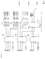
る。図1は、スロットマシンに設けられる基板の正面図である。なお、以下の実施形態に
おいて、「上」「下」「左」「右」「後(奥)」「前(手前)」の各方向について、基板
1がスロットマシンの筐体に取り付けられた状態に基づいて説明する。また、面の向き(
方向)とは、その面に直交する軸の延在方向であってその面を視認する側の方向とする。
例えば、図1において、「型番100」と記載された主要回路10の前面10Fは、前方
が面の向きとなる。また、文字の向きは、その文字を見る者が、所定の一方向からその文
字を読みやすくなるか否かが定められる向きである。例えば、3つの文字が左右方向に標
準的に並んで記載されている場合に、その中央の文字が180°回転していたら、その中
央の文字は他の2つの文字と文字の向きが異なっており、その他の2つの文字は互いに向
きが共通する。
A mode for carrying out a gaming machine, which is an example of the gaming machine according to the present invention, will be described below. In the following embodiments, the ratios and the like of each drawing may differ from the actual ratios and the like. FIG. 1 is a front view of a board provided in a slot machine. In the following embodiments, the
The direction) is the extending direction of the axis orthogonal to the surface and is the direction on the side where the surface is visually recognized.
For example, in FIG. 1, the
例えば、3次元空間において、互いに直交する3つの面、前後方向に沿った第1軸に直
交する第1面、上下方向に沿った第2軸に直交する第2面、及び左右方向に沿った第3軸
に直交する第3面を想定する。この場合、第1面は、前方(手前側)または後方(奥側)
を向き、第2面は、上方(上側)または下方(下側)を向き、第3面は右方(右側)また
は左方(左側)を向くことになる。
For example, in three-dimensional space, three planes orthogonal to each other, a first plane orthogonal to the first axis along the front-back direction, a second plane orthogonal to the second axis along the vertical direction, and along the left-right direction. Assume a third plane orthogonal to the third axis. In this case, the first surface is the front (front side) or the rear (back side).
The second surface faces upward (upper side) or lower side (lower side), and the third surface faces right side (right side) or left side (left side).
また、文字の向きは、文字が記載される面の向きによって制限される。例えば、第1面
に記載される文字は、前方(手前側)または後方(奥側)を成分とする方向を向くことは
なく、例えば、上方(上側)、下方(下側)、左方(左側)、及び右方(右側)のいずれ
か、あるいは、これらの各方向の成分を掛け合わせた方向、例えば右上方、左下方などと
なる。また、第2面に記載される文字は、上方(上側)または下方(下側)を成分とする
方向を向くことはなく、例えば、前方(手前側)、後方(奥側)、左方(左側)、及び右
方(右側)のいずれか、あるいは、これらの各方向の成分を掛け合わせた方向、例えば右
前方、左後方などとなる。また、第3面に記載される文字は、右方(右側)または左方(
左側)を成分とする方向を向くことはなく、例えば、上方(上側)、下方(下側)、前方
(手前側)、及び後方(奥側)のいずれか、あるいは、これらの各方向の成分を掛け合わ
せた方向、例えば上前方、下後方などとなる。
In addition, the orientation of the characters is limited by the orientation of the surface on which the characters are written. For example, the characters described on the first surface do not face the direction in which the front (front side) or the rear (back side) is a component, and for example, the upper side (upper side), the lower side (lower side), and the left side ( Either the left side) or the right side (right side), or the direction obtained by multiplying the components in each of these directions, for example, the upper right side, the lower left side, and the like. In addition, the characters written on the second surface do not face the direction in which the upper (upper side) or lower (lower side) is a component, and for example, the front side (front side), the rear side (back side), and the left side ( Either the left side) or the right side (right side), or the direction obtained by multiplying the components in each of these directions, for example, the front right, the rear left, and the like. In addition, the characters written on the third surface are on the right (right side) or left side (on the right side).
It does not face the direction of the component (left side), for example, one of the upper (upper), lower (lower), front (front), and rear (back), or the component in each of these directions. The direction in which they are multiplied, for example, the upper front, the lower rear, and the like.
基板1は、図示しない基板ケースに収容され、遊技機であるスロットマシンの筐体の内
部に設けられている。基板1は、図1に示すように、広い面(電子部品の実装面)が前面
を向くようにして配置され、スロットマシンの筐体の内側における奥方の板の手前側の面
に固定されて取り付けられる。また、基板ケースは透明の素材で設けられており、基板ケ
ースの外側から基板1が視認できるようにされている。
The
基板1は、スロットマシンの遊技を主に司るいわゆる主基板であり、図1に示すように
、基板部材2と、基板部材2に搭載された多数の電子部品を備えている。具体的に、基板
部材2の一面側には、1個の主要回路10が実装されている。主要回路10は、回路素子
であり、遊技の制御を行う特別電子部品である。また、基板部材2には、上第1出力回路
11A、中第1出力回路11B、下第1出力回路11Cの3個の第1出力回路が実装され
ている。上第1出力回路11A、中第1出力回路11B、下第1出力回路11Cは、互い
に同一種類の回路によって構成されている。上第1出力回路11A、中第1出力回路11
B、下第1出力回路11Cは、文字が記された複数の特定電子部品である。上第1出力回
路11A、中第1出力回路11B、下第1出力回路11Cに記載された文字については、
後に説明する。
The
B, the lower
It will be explained later.
これらの上第1出力回路11A、中第1出力回路11B、下第1出力回路11Cは、互
いに同一種類の電子部品である。なお、以下の説明において、同一種類の電子部品につい
ては、その共通する性質に即した説明をする場合には、符号の語尾に付されたアルファベ
ットを省略して、それらの説明を行うことがある。例えば、共通する電子部品である上第
1出力回路11A、中第1出力回路11B、下第1出力回路11Cについて共通する性質
を説明する際には、第1出力回路11としての性質等を説明することがある。
The upper
また、基板部材2の一面側には、右上第2出力回路12A、右下第2出力回路12B、
及び左第2出力回路12Cの3個の第2出力回路12が実装され、第3出力回路13Aの
1個の第3出力回路13が実装され、上第4出力回路14A及び下第4出力回路14Bの
2つの第4出力回路14が実装され、第5出力回路15Aの1個の第5出力回路15が実
装されている。このうち、右上第2出力回路12A、右下第2出力回路12B、及び左第
2出力回路12Cは、互いに同一種類の電子部品によって構成されている。また、上第4
出力回路14A及び下第4出力回路14Bも同一種類の電子部品によって構成されている
。また、第2出力回路12と第3出力回路13Aは互いに近傍位置となるように配置され
ている。
Further, on one side of the
And three
The
また、基板部材2の一面側には、右第1入力回路21A、中第1入力回路21B、及び
左第1入力回路21Cの3つの第1入力回路が実装されている。右第1入力回路21A、
中第1入力回路21B、及び左第1入力回路21Cは、互いに同一種類の電子部品によっ
て構成されている。また、第1入力回路21は、第3出力回路13と同一種類の電子部品
によって構成されている。これらの第3出力回路13及び第1入力回路21は、識別部品
回路となる。これらの第1出力回路11~第5出力回路15及び第1入力回路21は、い
ずれも回路素子である。また、第1出力回路11~第5出力回路15は、所定電子部品で
ある。
Further, three first input circuits, a right
The middle
また、基板部材2の一面側には、第1抵抗素子31~第8抵抗素子38が並設されてお
り、第8抵抗素子38における第7抵抗素子37の反対側に、異性能抵抗素子41が並設
されている。第1抵抗素子31~第8抵抗素子38、及び異性能抵抗素子41は、いずれ
も極性のない2つの端子を備える電子部品であり、抵抗値が共通する同一性能の抵抗素子
である。
Further, the
また、基板部材2の一面側には、第1セグメント表示部51~第4セグメント表示部5
4、電源確認ランプ55が実装されれている。第1セグメント表示部51は、複数の端子
を有する特殊電子部品であり、「8」の数字をかたどる7個のセグメントからなるいわゆ
る7セグメントと、7セグメントの右下に配置された1つの丸型セグメントの合計8個の
セグメントを備えている。第2セグメント表示部52~第4セグメント表示部54も、同
様に配置された8個のセグメントを備えている。電源確認ランプ55は、1個の丸型ラン
プを備えて構成されている。
Further, on one surface side of the
4. The power
さらに、基板部材2の一面側には、第1入出力端子61、第2入出力端子62、及び第
3入出力端子63が実装されている。第1入出力端子61、第2入出力端子62、及び第
3入出力端子63は、互いに異種の入出力端子である。第1入出力端子61、第2入出力
端子62、及び第3入出力端子63は、基板部材2の下端部において、右から順に並んで
配置されている。
Further, a first input /
第1セグメント表示部51~第4セグメント表示部54には、役比表示手段であり、主
要回路10から送信される信号に応じて、役比(役物比率)に関する数値を表示する。電
源確認ランプ55は、電源がONとなったときに点灯し、電源がOFFとなったときに消
灯する。第1入出力端子61~第3入出力端子63には、スロットマシンに設けられる種
々の部品との間における信号を送受信する配線が接続されている。
The first
基板部材2の一面側に設けられたこれらの電子部品は、基板部材2の一面側及び他面側
(裏面側)、さらには基板部材2に設けられたスルーホール等で配線を介して接続されて
いる。これらの配線については図示を省略する。また、基板部材2には、図1に示した電
子部品以外の電子部品も実装されている。これらの電子部品については、文字等は記載さ
れていない。本実施形態では、これらの文字等が記載されていない電子部品についての説
明は省略する。
These electronic components provided on one side of the
また、これらの電子部品や基板部材2には、電子部品の種類や電子部品を搭載する位置
を示すための文字等が記載されている。具体的に、図2にも示すように、主要回路10の
前面10Fには、「型番100」の文字が表示されている。主要回路10の前面10Fは
、基板部材2における主要回路10の実装面と共通する方向を向いた面である。主要回路
10の前面に表示された文字は、例えばシルク印刷によって記載されている。主要回路1
0に記載された文字は、上を向いて表示されている。主要回路10の前面10Fに記載さ
れた「型番100」の文字は、他の電子部品に記載された文字よりも大きい文字とされて
いる。
Further, on these electronic components and the
The characters described in 0 are displayed facing upward. The characters of "model number 100" written on the
なお、以下の各電子部品に表示される文字(文字情報)は、いずれもシルク印刷によっ
て記載されている。また、各電子部品に表示される文字は、シルク印刷以外の印刷などの
手段で表示(記載)されていてもよい。また、これらの文字は、電子部品に直接印刷等で
記載されていてもよいし、文字が印刷(記載)されたシール等が貼着されることによって
表示されていてもよい。
The characters (character information) displayed on each of the following electronic components are described by silk printing. Further, the characters displayed on each electronic component may be displayed (described) by means such as printing other than silk printing. Further, these characters may be directly printed on the electronic component or the like, or may be displayed by affixing a sticker or the like on which the characters are printed (described).
また、各電子部品に表示される文字は、主要回路10に記載された文字のように漢字で
もよいし、その他の文字、例えばひらがな、カタカナ、算用数字、アルファベット、ロシ
ア文字、ギリシア文字等の文字でもよいし、これらの文字の組み合わせでもよい。さらに
は、記号などでもよいし、文字と記号を組み合わせたものでもよい。また、各電子部品に
表示される文字は、そのロット番号などの電子部品自体に関する記述内容でもよいし、各
電子部品が用いられる用途(例えば「出力回路」等)などでもよい。
Further, the characters displayed on each electronic component may be Chinese characters such as the characters described in the
また、図3に示すように、上第1出力回路11Aの下面11AL、中第1出力回路11
Bの下面11BL、及び下第1出力回路11Cの下面11CLのには、いずれも「型番1
」の文字が表示されている。上第1出力回路11Aの下面11ALに表示された文字は、
所定の一方向からその文字を見る者が読みやすい向き(以下、単に「読みやすい向き」と
もいう)を向くように表示されている。中第1出力回路11Bの下面11BL及び下第1
出力回路11Cの下面11CLに表示された文字についても、上第1出力回路11Aの下
面11ALに表示された文字と同一の方向を向いている。また、上第1出力回路11Aの
下面11AL、中第1出力回路11Bの下面11BL、及び下第1出力回路11Cの下面
11CLにそれぞれ記載された「型番1」の文字の形状及び大きさは、互いに略同一であ
る。
Further, as shown in FIG. 3, the lower surface 11AL of the upper
The lower surface 11BL of B and the lower surface 11CL of the lower
Character is displayed. The characters displayed on the lower surface 11AL of the upper
It is displayed so that a person who sees the character from a predetermined direction faces an easy-to-read direction (hereinafter, also simply referred to as "easy-to-read direction"). The lower surface 11BL and the lower first of the middle
The characters displayed on the lower surface 11CL of the
基板部材2における上第1出力回路11Aの近傍位置、具体的には、上第1出力回路1
1Aの右下部には、図1及び図3に示すように、「型番1」の文字が表示されている。こ
の「型番1」の文字は、読みやすい向きを向いている。また、この「型番1」の文字は、
上第1出力回路11Aに記載された「型番1」の文字よりも小さい文字とされている。な
お、本実施形態では、基板部材2における上第1出力回路11Aの近傍位置に記載された
文字は、「型番1」であり、上第1出力回路11Aに記載された文字と同一であるが、他
の文字、例えば、上第1出力回路11Aに記載された文字と関連する文字であってもよい
。例えば、第1出力回路11に記載された「型番1」の文字を簡略化し、「型番」の頭文
字をとって「K1」などとした文字であってもよい。あるいは、電子部品について機能や
種類に分けてそれぞれに通し番号を付し、これらの通し番号を電子部品の近傍位置に記載
する文字としてもよい。このときの通し番号は、電子部品の一部に付してもよいし、全部
に付してもよい。電子部品の一部に付する場合には、複数系統に分けて(例えば「A1」
「A2」・・・と「B1」[B2]・・・等)、通し番号を付してもよい。あるいは、入
力回路には頭文字「I」、入力回路には頭文字の「O」を付加するなどの規則付けを行い
、上第1出力回路11Aの近傍に記載された文字を「上1OA」もしくは「U1OA」な
どとしてもよい。基板部材2における上第1出力回路11Aの近傍位置に記載された文字
は、上第1出力回路11Aに記載された文字数よりも数が少ない文字数となるようにして
もよいし、多い文字数となるようにしてもよい。
The position near the upper
As shown in FIGS. 1 and 3, the characters "
The characters are smaller than the characters of "
"A2" ... And "B1" [B2] ... etc.), Serial numbers may be assigned. Alternatively, a rule such as adding an acronym "I" to the input circuit and an acronym "O" to the input circuit is applied, and the character written in the vicinity of the upper
また、主要回路10に表示された文字と、第1出力回路11の下面11Lに表示された
文字とを比較すると、いずれも基板1の主要回路10及び第1出力回路11に記載された
文字を見る者が、所定の一方向、例えば下側から見たときに、視点に近い側に文字の下部
が位置しており、その意味で特定の向きとなるように表示されている。言い換えると、こ
こでいう特定の向きとは、基板1を一方向から見たときに、その文字等の同じ側、例えば
下側が視点に近い側に位置する向きをいう。特定の向きは、同じ向きの面に表示されるこ
ともあるが、上記のように、異なる向きの面に表示された文字のそれぞれの向きが特定の
向きとなることもある。
Further, when the characters displayed on the
また、基板部材2における上第1出力回路11Aの近傍位置と同様に、基板部材2にお
ける中第1出力回路11B及び下第1出力回路11Cの近傍の右下部は、いずれも「型番
1」の文字が読みやすい向きで表示されている。この「型番1」の文字は、上第1出力回
路11Aの近傍位置に表示された「型番1」の文字と同じ形状であるが、大きさは小さく
されている。なお、基板部材2における他の電子部品の近傍にも同様に、各電子部品と同
一の文字が記載されているが、その説明は省略する。
Further, similarly to the position near the upper
図1及び図2に示すように、右上第2出力回路12Aの前面12AF、右下第2出力回
路12Bの前面12BF、及び左第2出力回路12Cの前面12CFには、それぞれ「型
番2」の文字が表示されている。右上第2出力回路12Aの前面12AF、右下第2出力
回路12Bの前面12BF、及び左第2出力回路12Cの前面12CFにそれぞれ記載さ
れた文字は、それぞれ所定の一方向からその文字を見る者が読みにくい向き(以下、単に
「読みにくい向き」ともいう)で記載されている。また、右上第2出力回路12Aの前面
12AF、右下第2出力回路12Bの前面12BF、及び左第2出力回路12Cの前面1
2CFにそれぞれ記載された「型番2」の文字の大きさは、互いに略同一である。また、
「型番2」の文字が記載された第2出力回路12の前面12Fは、主要回路10における
「型番100」の文字が記載された前面10Fと共通する方向を向いた面である。
As shown in FIGS. 1 and 2, the front surface 12AF of the upper right
The size of the characters of "
The front surface 12F of the
図1及び図2に示すように、第3出力回路13Aの前面13AFには、「型番3」の文
字が表示されている。第3出力回路13Aの前面13AFに表示された文字は、読みにく
い向きで記載されている。また、第3出力回路13Aの前面13AFに表示された「型番
3」の文字の大きさは、右上第2出力回路12Aの前面12AF、右下第2出力回路12
Bの前面12BF、及び左第2出力回路12Cの前面12CFにそれぞれ表示された「型
番2」の文字の形状および大きさと略同一である。また、「型番3」の文字が記載された
第3出力回路13Aの前面13AFは、主要回路10における「型番100」の文字が記
載された前面10Fと共通する方向を向いた面である。
As shown in FIGS. 1 and 2, the characters "
It is substantially the same as the shape and size of the characters of "
また、第2出力回路12の前面12Fと、第3出力回路13Aの前面13AFに記載さ
れた文字はいずれも読みにくい向きで表示されている。第3出力回路13Aが第1種類の
識別電子部品であるのに対して、第2出力回路12(右上第2出力回路12A、右下第2
出力回路12B、左第2出力回路12C)は、第1所定電子部品となる。
Further, the characters written on the front surface 12F of the
The
図1~図3に示すように、上第4出力回路14Aの前面14AF及び下第4出力回路1
4Bの前面14BFには、それぞれ「型番4」の文字が表示されている。上第4出力回路
14Aの前面14AF及び下第4出力回路14Bの前面14BFに表示された文字は、そ
れぞれ読みにくい向きで記載されている。また、上第4出力回路14Aの前面14AF及
び下第4出力回路14Bの前面14BFにそれぞれ記載された「型番4」の文字の大きさ
は、右上第2出力回路12Aの前面12AF、右下第2出力回路12Bの前面12BF、
及び左第2出力回路12Cの前面12CFにそれぞれ表示された「型番2」の文字の形状
および大きさと略同一である。また、「型番4」の文字が記載された第4出力回路14の
前面14Fは、主要回路10における「型番100」の文字が記載された前面10Fと共
通する方向を向いた面である。
As shown in FIGS. 1 to 3, the front surface 14AF of the upper
The characters "
And the shape and size of the characters of "
図1及び図2に示すように、第5出力回路15Aの前面15AFには、「型番5」の文
字が表示されている。第5出力回路15Aの前面15AFに表示された文字は、読みにく
い向きで記載されている。また、第5出力回路15Aの前面15AFに表示された「型番
5」の文字の大きさは、右上第2出力回路12Aの前面12AF、右下第2出力回路12
Bの前面12BF、及び左第2出力回路12Cの前面12CFにそれぞれ表示された「型
番2」の文字の形状および大きさと略同一である。また、「型番5」の文字が記載された
第5出力回路15の前面15Fは、主要回路10における「型番100」の文字が記載さ
れた前面10Fと共通する方向を向いた面である。
As shown in FIGS. 1 and 2, the characters "
It is substantially the same as the shape and size of the characters of "
図1及び図2に示すように、右第1入力回路21Aの前面21AF、中第1入力回路2
1Bの前面21BF、及び左第1入力回路21Cの前面21CFには、それぞれ「型番3
」の文字が表示されている。右第1入力回路21Aの前面21AF、中第1入力回路21
Bの前面21BF、及び左第1入力回路21Cの前面21CFに表示された文字は、それ
ぞれ読みやすい向きで記載されている。また、右第1入力回路21Aの前面21AF、中
第1入力回路21Bの前面21BF、及び左第1入力回路21Cの前面21CFにそれぞ
れ記載された「型番3」の文字の大きさは、右上第2出力回路12Aの前面12AF、右
下第2出力回路12Bの前面12BF、及び左第2出力回路12Cの前面12CFにそれ
ぞれ表示された「型番2」の文字の形状および大きさと略同一である。また、「型番3」
の文字が記載された第1入力回路21の前面21Fは、主要回路10における「型番10
0」の文字が記載された前面10Fと共通する方向を向いた面である。
As shown in FIGS. 1 and 2, the front surface 21AF of the right
The front surface 21BF of 1B and the front surface 21CF of the left
Character is displayed. Front 21AF of right
The characters displayed on the front surface 21BF of B and the front surface 21CF of the left
The front surface 21F of the
It is a surface facing the same direction as the
また、第3出力回路13の前面に記載された文字の向きは、読みにくい向きとなってお
り、第1入力回路21の前面に記載された文字の向きは、読みやすい向きとなっている。
第3出力回路13と第1入力回路21とでは、同一種類の電子部品(識別電子部品)が使
用されているが、それぞれの前面に記載された文字の向きを互いに反転させて異なる向き
となるようにすることで、第3出力回路13と第1入力回路21を外見から識別できるよ
うにされている。第3出力回路13は、第1種類の識別電子部品であり、第1入力回路2
1は第2識別電子部品である。
Further, the orientation of the characters written on the front surface of the
Although the same type of electronic component (identification electronic component) is used in the
図4に示すように、第1抵抗素子31には、下から順に第1ラインL1、第2ラインL
2、第3ラインL3、及び第4ラインL4からなる第1カラーコードCC1が所定のマー
クとして描かれている。第1カラーコードCC1における第1ラインL1~第4ラインL
4は、互いに異なる色として描かれている。また、第2抵抗素子32~第8抵抗素子38
においても、同様の第1ラインL1~第4ラインL4からなる第1カラーコードCC1が
描かれている。第1抵抗素子31~第8抵抗素子38は、第1カラーコードCC1(第1
ラインL1~第4ラインL4)は、所定のマークの向きが共通するように、それぞれ一直
線上に整列して配置されるように、並べられている。
As shown in FIG. 4, the
2. The first color code CC1 including the third line L3 and the fourth line L4 is drawn as a predetermined mark. 1st line L1 to 4th line L in the 1st color code CC1
4 is drawn as different colors from each other. Further, the
Also in the above, the first color code CC1 composed of the same first line L1 to fourth line L4 is drawn. The
The lines L1 to the fourth line L4) are arranged so as to be aligned and arranged in a straight line so that the directions of the predetermined marks are common.
また、第8抵抗素子38に並べられた異性能抵抗素子41には、第5ラインL5~第8
ラインL8からなる第2カラーコードCC2が描かれている。異性能抵抗素子41の第2
カラーコードCC2となる第5ラインL5~第8ラインL8は、第1抵抗素子31~第8
抵抗素子38の第1カラーコードCC1となる第1ラインL1~第4ラインL4とでは、
配色が互いに異なっている。また、第1抵抗素子31~第8抵抗素子38の第1カラーコ
ードCC1(第1ラインL1~第4ラインL4)と異性能抵抗素子41の第2カラーコー
ドCC2(第5ラインL5~第8ラインL8)とでは、第1ラインL1と第5ラインL5
、第2ラインL2と第6ラインL6、第3ラインL3と第7ラインL7、第4ラインL4
と第8ラインL8は、それぞれ互いに一直線上に配置されている。第1抵抗素子31~第
8抵抗素子38に描かれた第1カラーコードCC1及び異性能抵抗素子41に描かれた第
2カラーコードCC2は、例えば、抵抗素子の性能表示、例えば抵抗値及び許容差に応じ
て描かれるラインである。このため、第1抵抗素子31~第8抵抗素子38、及び異性能
抵抗素子41は、いずれも抵抗素子としての種類が同一の電子部品であるが、その性能は
異なっている。
Further, the different
A second color code CC2 consisting of line L8 is drawn. The second of the different
The fifth line L5 to the eighth line L8, which is the color code CC2, are the
In the first line L1 to the fourth line L4, which is the first color code CC1 of the
The color schemes are different from each other. Further, the first color code CC1 (first line L1 to fourth line L4) of the
, 2nd line L2 and 6th line L6, 3rd line L3 and 7th line L7, 4th line L4
And the eighth line L8 are arranged in a straight line with each other. The first color code CC1 drawn on the
また、図1及び図3に示すように、基板部材2の一面側において、右側の位置に上第1
出力回路11A、中第1出力回路11B、下第1出力回路11Cが上下方向に並んで設け
られている。これらの上第1出力回路11A、中第1出力回路11B、下第1出力回路1
1Cの左隣に、右上第2出力回路12A及び右下第2出力回路12Bが上下に並んで配置
されている。右上第2出力回路12Aは、高さ方向に見て、上第1出力回路11Aと中第
1出力回路11Bの間に配置されている。右下第2出力回路12Bは、高さ方向に見て、
中第1出力回路11Bと下第1出力回路11Cの間に配置されている。
Further, as shown in FIGS. 1 and 3, on the one side of the
The
The upper right
It is arranged between the middle
右下第2出力回路12Bの左隣には、左第2出力回路12Cが配置されている。左第2
出力回路12Cは、右下第2出力回路12Bの高さ位置と略同じ高さ位置に配置されてい
る。左第2出力回路12Cの直下には、第3出力回路13Aが配置されている。第3出力
回路13Aは、下第1出力回路11Cよりも低い位置に配置されている。
The left
The
左第2出力回路12Cの左隣には、上第4出力回路14Aが配置され、第3出力回路1
3Aの左隣には、下第4出力回路14Bが配置されている。上第4出力回路14A及び下
第4出力回路14Bは、それぞれ左第2出力回路12C及び第3出力回路13Aと略同じ
高さ位置に配置されている。
The upper
The lower
上第4出力回路14A及び下第4出力回路14Bの左隣には、右第1入力回路21A及
び第5出力回路15Aが配置されている。右第1入力回路21Aは、上第4出力回路14
Aよりも高い位置に配置されている。第5出力回路15Aは、上第4出力回路14Aより
も低い位置であり、下第4出力回路14Bよりも高い位置に配置されている。
The right
It is located higher than A. The
第5出力回路15Aの左下位置には、中第1入力回路21Bが配置され、中第1入力回
路21Bの左側には、左第1入力回路21Cが配置されている。中第1入力回路21Bは
、下第4出力回路14Bよりも低い位置に配置されており、左第1入力回路21Cは、中
第1入力回路21Bと略同じ高さ位置に配置されている。
The middle
また、上第4出力回路14Aの直上位置に、第1抵抗素子31~第8抵抗素子38、さ
らには異性能抵抗素子41が配置されている。また、左第1入力回路21Cの上方には、
主要回路10が配置されており、右第1入力回路21Aの直上位置には、第1セグメント
表示部51~第4セグメント表示部54が配置され、第4セグメント表示部54の右隣に
電源確認ランプ55が配置されている。
Further, the
The
また、基板部材2の一面側の下端部には、右から順に第1入出力端子61、第2入出力
端子62、及び第3入出力端子63が配置されている。このうち、第1入出力端子61は
、右下第2出力回路12Bの下方位置に配置されている。第2入出力端子62は、左第1
入力回路21Cの下方位置に配置されている。第3入出力端子63は、第2入出力端子6
2のさらに左側に配置されている。
Further, a first input /
It is located below the
It is located further to the left of 2.
次に、各電子部品やスロットマシンに設けられた各部品の接続及び信号の入出力先につ
いて、図5~図8を参照して説明する。図5(A)に示すように、第3入出力端子63に
は、遊技メダル払出センサ1から「MEOUTS1」、遊技メダル払出センサ2から「M
EOUTS2」、設定キースイッチから「LVKEYSW」、設定/リセットスイッチか
ら「LV/RSTW」、遊技メダル補助収納庫センサから「OVERSW」の各信号が入
力される。第3入出力端子63は、入力されたこれらの各信号を図6に示す左第1入力回
路21C及び中第1入力回路21Bに出力する。また、第3入出力端子63には、電源装
置から電源が供給され、第3入出力端子63を介して基板1における各電子部品に電流が
供給される。左第1入力回路21C及び中第1入力回路21Bには、例えばメダルの投入
や払出、スロットマシンの設定などに関する情報が入力される。
Next, the connection of each electronic component and each component provided in the slot machine and the input / output destination of the signal will be described with reference to FIGS. 5 to 8. As shown in FIG. 5A, the third input /
Each signal of "EOUTS2", "LVKEYSW" from the setting key switch, "LV / RSTW" from the setting / reset switch, and "OVERSW" from the game medal auxiliary storage sensor is input. The third input /
図5(B)に示すように、第1入出力端子61には、第1回胴センサから「ORGSE
N1」、第2回胴センサから「ORGSEN2」、第3回胴センサから「ORGSEN3
」、の各信号が入力される。第1入出力端子61は、入力されたこれらの各信号を図6に
示す右第1入力回路21Aに出力する。右第1入力回路21Aには、例えばスロットマシ
ンのリールに関する情報が入力される。
As shown in FIG. 5B, the first input /
"N1", "ORGSEN2" from the 2nd body sensor, "ORGSEN3" from the 3rd body sensor
,, Each signal is input. The first input /
図5(C)に示すように、第2入出力端子62には、精算スイッチから「PAY」、M
AXBETスイッチから「MBET」、第1回胴停止スイッチから「SPSW1」、第2
回胴停止スイッチから「SPSW2」、第3回胴停止スイッチから「SPSW3」、遊技
メダルセンサ1から「SEN1」、遊技メダルセンサ2から「SEN2」、遊技メダルセ
ンサ3から「SEN3」、ドアセンサから「DOOR」、ドアリセットから「RESET
」の各信号が入力される。第2入出力端子62は、入力されたこれらの各信号を図6に示
す右第1入力回路21A、中第1入力回路21B、及び左第1入力回路21Cに出力する
。右第1入力回路21A、中第1入力回路21B、及び左第1入力回路21Cには、例え
ば遊技者や店員などがスロットマシンについて操作するスイッチに関する情報が入力され
る。
As shown in FIG. 5C, the second input /
"MBET" from the AXBET switch, "SPSW1" from the 1st body stop switch, 2nd
"SPSW2" from the rotation stop switch, "SPSW3" from the 3rd body stop switch, "SEN1" from the
Each signal of "is input. The second input /
図5(D)に示すように、図示しない電源装置に対して、電源確認ランプ55が接続さ
れており、電源確認ランプ55と電源装置の間には、異性能抵抗素子41が介在されてい
る。異性能抵抗素子41は、電源確認ランプ55に接続されている。電源確認ランプ55
は、電源装置によってスロットマシンの電源がONとなったときに電流が供給されて点灯
し、電源装置によってスロットマシンの電源がOFFとなったときに電流の供給が停止し
て消灯する。異性能抵抗素子41は、電源確認ランプ55に供給される電流を減圧してい
る。
As shown in FIG. 5D, a power
Is turned on by supplying a current when the power of the slot machine is turned on by the power supply device, and is turned off by stopping the supply of the current when the power of the slot machine is turned off by the power supply device. The different
図6に示すように、右第1入力回路21A、中第1入力回路21B、及び左第1入力回
路21Cは、第1入出力端子61、第2入出力端子62、及び第3入出力端子63から出
力された各信号の調圧や整流などの処理を行ってを主要回路10に出力する。主要回路1
0は、右第1入力回路21A、中第1入力回路21B、及び左第1入力回路21Cから出
力された各信号に基づいて演算処理を施して、スロットマシンを制御するための各信号を
生成し、図7及び図8に示す出力回路に出力する。
As shown in FIG. 6, the right
0 performs arithmetic processing based on each signal output from the right
具体的に、主要回路10は、図7に示す右上第2出力回路12Aに「K1MOTOR0
」、「K1MOTOR1」、「K1MOTOR2」、「K1MOTOR3」、「K2MO
TOR0」、「K2MOTOR1」、「K2MOTOR2」、「K2MOTOR3」、「
OUTF3」の各信号を出力する。これらの各信号は、一部を除いて右上第2出力回路1
2A、上第1出力回路11A、及び中第1出力回路11Bにおいて調圧や整流などの処理
が行われ、図5(B)に示す第1入出力端子61に出力される。第1入出力端子61から
は、「K1MOTOR0」が第1回胴モータΦ0、「K1MOTOR1」が第1回胴モー
タΦ1、「K1MOTOR2」が第1回胴モータΦ2、「K1MOTOR3」が第1回胴
モータΦ3にそれぞれ出力される。また、「K2MOTOR0」が第2回胴モータΦ0、
「K2MOTOR1」が第2回胴モータΦ1、「K2MOTOR2」が第2回胴モータΦ
2、「K2MOTOR3」が第2回胴モータΦ3にそれぞれ出力される。右上第2出力回
路12A、上第1出力回路11A、及び中第1出力回路11Bは、例えばスロットマシン
のリール停止に関する信号を出力する。
Specifically, the
, "K1MOTOR1", "K1MOTOR2", "K1MOTOR3", "K2MO"
TOR0 ”,“ K2MOTOR1 ”,“ K2MOTOR2 ”,“ K2MOTOR3 ”,“
Each signal of "OUTF3" is output. Each of these signals is the upper right
Processing such as pressure regulation and rectification is performed in 2A, the upper
"K2MOTOR1" is the 2nd cylinder motor Φ1, "K2MOTOR2" is the 2nd cylinder motor Φ
2. "K2MOTOR3" is output to the 2nd body motor Φ3, respectively. The upper right
主要回路10は、図7に示す右下第2出力回路12Bに「K3MOTOR0」、「K3
MOTOR1」、「K3MOTOR2」、「K3MOTOR3」、「OUTF4」の各信
号を出力する。これらの各信号は、一部を除いて右下第2出力回路12B及び下第1出力
回路11Cにおいて調圧や整流などの処理が行われ、図5(B)に示す第2入出力端子6
2に出力される。第2入出力端子62からは、「K3MOTOR0」が第3回胴モータΦ
0、「K3MOTOR1」が第3回胴モータΦ1、「K3MOTOR2」が第3回胴モー
タΦ2、「K3MOTOR3」が第3回胴モータΦ3にそれぞれ出力される。右下第2出
力回路12B及び下第1出力回路11Cは、例えばスロットマシンのリール停止に関する
信号を出力する。
The
Each signal of "MOTOR1", "K3MOTOR2", "K3MOTOR3", and "OUTF4" is output. Except for a part, each of these signals is subjected to processing such as pressure regulation and rectification in the lower right
It is output to 2. From the 2nd input /
0, "K3MOTOR1" is output to the 3rd cylinder motor Φ1, "K3MOTOR2" is output to the 3rd cylinder motor Φ2, and "K3MOTOR3" is output to the 3rd cylinder motor Φ3. The lower right
主要回路10は、図7に示す左第2出力回路12Cに「SPLED1」、「SPLED
2」、「SPLED3」、「MAXLED」、「BLK」、「K1COM」、「K2CO
M」、「K3COM」、「RST」、「OUTF5」の各信号を出力する。これらの各信
号は、一部を除いて左第2出力回路12C及び第3出力回路13A等において調圧や整流
などの処理が行われる。これらの各信号のうち、「SPLED1」、「SPLED2」、
「SPLED3」、「MAXLED」は、図5(C)に示す第2入出力端子62に出力さ
れ、「BLK」「K1COM」、「K2COM」、「K3COM」は、図5(B)に示す
第1入出力端子61に出力される。第2入出力端子62からは、「SPLED1」が第1
回胴停止LED、「SPLED2」が第2回胴停止LED、「SPLED3」が第3回胴
停止LED、「MAXLED」がMAXBETLEDにそれぞれ出力される。第1入出力
端子61からは、「BLK」が遊技メダルブロッカ、「K1COM」が第1モータコモン
、「K2COM」が第2モータコモン、「K3COM」が第3モータコモンにそれぞれ出
力される。左第2出力回路12C及び第3出力回路13Aは、例えば遊技者が視認するラ
ンプの点灯・点滅等に関する信号を出力する。
The
2 ”,“ SPLED3 ”,“ MAXLED ”,“ BLK ”,“ K1COM ”,“ K2CO ”
Each signal of "M", "K3COM", "RST", "OUTF5" is output. Except for a part, each of these signals is subjected to processing such as pressure regulation and rectification in the left
"SPLED3" and "MAXLED" are output to the second input /
The rotation stop LED, "SPLED2" are output to the second body stop LED, "SPLED3" is output to the third body stop LED, and "MAXLED" is output to the MAXBETLED. From the first input /
主要回路10は、図8に示す下第4出力回路14Bに「SEGa」、「SEGb」、「
SEGc」、「SEGd」、「SEGe」、「SEGf」、「SEGg」、「OUTF7
」の各信号を出力する。これらの各信号は、一部を除いて下第4出力回路14Bにおいて
調圧や整流などの処理が行われ、図5(C)に示す第2入出力端子62に出力される。第
2入出力端子62からは、「SEGa」が投入枚数1LED、「SEGb」が投入枚数2
LED、「SEGc」が投入枚数3LED、「SEGd」が再遊技表示LED、「SEG
e」が演出表示LED、「SEGf」が遊技開始表示LED、「SEGg」が投入可能表
示LEDの7セグにそれぞれ出力される。下第4出力回路14Bは、例えば遊技者が視認
するランプの点灯・点滅等に関する信号を出力する。
The
SEGc ”,“ SEGd ”,“ SEGe ”,“ SEGf ”,“ SEGg ”,“ OUTF7
"Each signal is output. Except for a part, each of these signals is subjected to processing such as pressure regulation and rectification in the lower
LED, "SEGc" is the input number 3LED, "SEGd" is the replay display LED, "SEG"
"e" is output to the effect display LED, "SEGf" is output to the game start display LED, and "SEGg" is output to the 7-segment display LED that can be input. The lower
主要回路10は、図8に示す上第4出力回路14Aに「DG1」、「DG2」、「DG
3」、「DG4」、「DG5」、「DG6」、「OUTFA」の各信号を出力する。「D
G1」~「DG6」は、LED等のランプの点灯や点滅を管理するデジット信号である。
これらの各信号は、一部を除いて上第4出力回路14Aにおいて調圧や整流などの処理が
行われ、図5(C)に示す第2入出力端子62に出力される。第2入出力端子62からは
、「DG1」がDG1、「DG2」がDG2、「DG3」がDG3、「DG4」がDG4
、「DG5」がDG5、「DG6」がDG6にそれぞれ出力される。上第4出力回路14
Aは、例えばランプの点灯に関するデジット信号を出力する。
The
3 ”,“ DG4 ”,“ DG5 ”,“ DG6 ”, and“ OUTFA ”signals are output. "D
"G1" to "DG6" are digit signals that control the lighting and blinking of lamps such as LEDs.
Except for a part, each of these signals is subjected to processing such as pressure regulation and rectification in the upper
, "DG5" is output to DG5, and "DG6" is output to DG6. Upper
A outputs, for example, a digit signal relating to the lighting of the lamp.
主要回路10は、図8に示す第5出力回路15Aに第1セグメント表示部51~第4セ
グメント表示部54の各セグメントの点灯及び消灯(点滅)の制御を行う点灯制御信号送
信する。主要回路10では、スロットマシンにおける役比に関する数値が算出されており
、算出された数値等を第1セグメント表示部51~第4セグメント表示部54の各セグメ
ントを点灯、消灯させるとによって表示する。このため、主要回路10は、第1セグメン
ト表示部51~第4セグメント表示部54の各セグメントを点灯させるための点灯制御信
号を第5出力回路15Aに出力し、第5出力回路15Aから第1セグメント表示部51~
第4セグメント表示部54に出力する。第5出力回路15Aは、例えば遊技者が視認する
ランプの点灯・点滅等に関する信号を出力する。
The
Output to the 4th
第5出力回路15と第1セグメント表示部51~第4セグメント表示部54の間には、
第1抵抗素子31~第8抵抗素子38が配置されている。第1抵抗素子31~第8抵抗素
子38は、第5出力回路15及び第1セグメント表示部51~第4セグメント表示部54
に接続されている。第5出力回路15Aから第1セグメント表示部51~第4セグメント
表示部54に出力される各セグメントに点灯制御信号は、第1抵抗素子31~第8抵抗素
子38によって各セグメントに表示されるランプの光量等を調整するように調圧される。
Between the
The
It is connected to the. The lighting control signal for each segment output from the
以上のとおり、本実施形態に係る遊技機に設けられる基板1においては、複数の電子部
品のうち、第1出力回路11(上第1出力回路11A、中第1出力回路11B、下第1出
力回路11C)に記載された「型番1」の文字は、その下面11L(11AL,11BL
,11CL)に記載されている。このため、第1出力回路11を一方向、具体的には斜め
下方向(左斜め下方向または右斜め下方向)からを同時に見た場合に、下面11Lに記載
された「型番1」の文字を一気に視認することができる。したがって、基板1に正しい部
品が取り付けられていることを容易に確認することができる。
As described above, in the
, 11CL). Therefore, when the
また、これらの文字は、いずれも読みやすい向きで記載されており、各文字の向きが共
通とされている。このため、出力回路として同様の機能を有するとともに、同一の回路が
用いられている第1出力回路11を視認するにあたり、一方向、具体的には斜め下方向か
ら見た場合にいずれも「型番1」の文字を同一方向に視認することができる。したがって
、基板1に正しい部品が取り付けられていることを容易に確認することができる。
In addition, all of these characters are written in an easy-to-read orientation, and the orientation of each character is common. Therefore, when visually recognizing the
また、第1出力に記載された文字の向きは特定の向きとなっており、主要回路10に記
載されている「型番100」の文字も特定の向きを向いている。このため、基板1を一方
向、ここでは斜め下方向から見たときに、主要回路10の前面10Fに表示された「型番
100」の文字と、第1出力回路11の下面11Lに表示された「型番1」の文字をいず
れもその文字の下側からのぞき込む方向で見ることができる。このため、「型番100」
の文字を視認することによって主要回路10の取付を確認する際に、合わせて「型番1」
の文字も確認し、第1出力回路11の取付を確認しやすくすることができる。したがって
、基板に正しい部品が取り付けられていることを容易に確認することができる。
Further, the direction of the characters described in the first output is a specific direction, and the characters of "model number 100" described in the
When confirming the installation of the
It is possible to confirm the attachment of the
また、主要回路10と例えば第1入力回路21との関係においては、主要回路10の前
面10Fに「型番100」の文字が記載され、第1入力回路21の前面21Fに「型番3
」の文字が記載されている。また、「型番100」の文字と「型番3」の文字は、いずれ
も読みやすい向きで記載されている。このため、「型番100」の文字を視認することに
よって主要回路10の取付を確認する際に、合わせて「型番3」の文字も確認しやすくす
ることができる。したがって、基板に正しい部品が取り付けられていることを容易に確認
することができる。
Further, in the relationship between the
"Is written. Further, the characters "model number 100" and the characters "
また、基板1に搭載された電子部品において、文字が表示された電子部品のうち、半数
以上の電子部品、具体的には、主要回路10、上第1出力回路11A、中第1出力回路1
1B、下第1出力回路11C、右上第2出力回路12A、右下第2出力回路12B、第5
出力回路15A、右第1入力回路21A、中第1入力回路21B、左第1入力回路21C
は、記載された文字が特定の方向を向いている。このため、基板1を一方向から同時に見
た場合に、これらの電子部品に記載された文字を一気に視認することができる。したがっ
て、基板1に搭載された文字が記載された電子部品のうちの半数以上の電子部品について
、基板に正しい部品が取り付けられていることを主要回路10とともに容易に確認するこ
とができる。
Further, among the electronic components mounted on the
1B, lower
The written characters are oriented in a specific direction. Therefore, when the
また、基板部材2における第1出力回路11の実装位置の近傍には、「型番1」の文字
が記載されている。この「型番1」の文字は、第1出力回路11の下面11Lに記載され
た文字と同一である。したがって、基板部材2における第1出力回路11の実装位置の近
傍及び第1出力回路11の下面11Lにそれぞれ記載された「型番1」の文字を確認する
ことにより、第1出力回路11が基板部材2おける正しい位置に取り付けられていること
を容易に確認することができる。
Further, the characters "
また、基板部材2における第1出力回路11の実装位置の近傍に記載された「型番1」
の文字は、図9に示すように、第1出力回路11の下面11Lに記載された「型番1」の
文字よりも小さくされている。このため、基板部材2に多数の電子部品を配置した場合で
も、各電子部品に対応する文字を基板部材2により多く記載することができる。
Further, "
As shown in FIG. 9, the character of is smaller than the character of "
また、基板部材2における第1出力回路11の実装位置の近傍に記載された「型番1」
の文字は、特定の向きを向いており、第1出力回路11の下面11Lに記載された「型番
1」の文字と向きが共通する。このため、基板部材2に記載された「型番1」の文字と第
1出力回路11に記載された「型番1」の文字を容易に確認することができる。
Further, "
The character of is oriented in a specific direction, and has the same orientation as the character of "
また、本実施形態に係る遊技機に設けられる基板1においては、第3出力回路13と第
1入力回路21で同じ種類の回路が使用されている。このため、第3出力回路13と第1
入力回路21を見間違えやすくなる可能性がある。この点、本実施形態の基板1では、第
3出力回路13と第1入力回路21を外見から識別できるようにして基板部材2に搭載し
ている。具体的には、第3出力回路13に表示される「型番3」の文字を読みにくい向き
で記載し、第1入力回路21に表示される「型番3」の文字を読みやすい向きで記載して
、「型番3」の文字と「型番3」の文字を互いに反転させた関係としている。このため、
第3出力回路13と第1入力回路21には、同じ「型番3」の文字が記載されているもの
の、第3出力回路13と第1入力回路21を容易に識別することができ、基板に正しい部
品が取り付けられていることを容易に確認することができる。
Further, in the
There is a possibility that the
Although the
また、電子部品に型番等が記載される場合、通常、電子部品における所定の位置に型番
を記載する。この場合、電子部品の向きを変えるだけで電子部品に記載された文字の向き
を変えることができるので、第3出力回路13と第1入力回路21に記載された「型番3
」の向きは、容易に変えることができる。特に、電子部品が対称形または対称形に近い形
状であるときには、同じ又は近似する領域に対して、向きを変えた状態で電子部品を搭載
させることができる。
When a model number or the like is described on an electronic component, the model number is usually described at a predetermined position on the electronic component. In this case, since the direction of the characters written on the electronic component can be changed only by changing the direction of the electronic component, the "
The orientation of "" can be easily changed. In particular, when the electronic component has a symmetrical shape or a shape close to the symmetrical shape, the electronic component can be mounted in the same or similar region in a different direction.
また、第3出力回路13と第1入力回路21として用いられた回路部品は、出力回路と
入力回路の両方で用いられており、外観上は近似するものの、その用途が大きく異なって
いる。この点、第3出力回路13と第1入力回路21について、表示された文字の向きを
変えることによって外見から識別できるようにされているので、信号の入力に用いられる
電子部品と信号の出力に用いられる電子部品という用途の異なる電子部品を容易に区別す
ることができる。
Further, the circuit components used as the
また、基板1には、出力回路として、複数種類の電子部品としての回路が設けられてい
る。このうちの1つの種類である第2出力回路12のうちの左第2出力回路12Cと、他
の1つの種類である第3出力回路13では、記載された文字がいずれも読みにくい向きを
向いている。このため、記載されている文字が読みやすい向きを向く第1入力回路21と
の区別を行い易くすることができる。したがって、出力回路と入力回路という種類の異な
る電子部品を容易に区別することができ、基板に正しい部品が取り付けられていることを
容易に確認することができる。
Further, the
また、左第2出力回路12Cと第3出力回路13は、互いに近傍位置となるように基板
1に搭載されている。このため、出力回路(左第2出力回路12Cと第3出力回路13)
と入力回路(第1入力回路21)という種類の異なる電子部品を容易に区別することがで
き、基板に正しい部品が取り付けられていることを容易に確認することができる。
Further, the left
And the input circuit (first input circuit 21), which are different types of electronic components, can be easily distinguished, and it can be easily confirmed that the correct components are mounted on the board.
また、本実施形態に係る遊技機に設けられる基板1においては、基板1に第1抵抗素子
31~第8抵抗素子38が設けられており、第1抵抗素子31~第8抵抗素子38はそれ
ぞれ第1セグメント表示部51~第4セグメント表示部54に接続されている。第1セグ
メント表示部51~第4セグメント表示部54は、役比を表示する装置であり、第1セグ
メント表示部51~第4セグメント表示部54に表示される数値は、非常に重要性の高い
数値である。このような重要性の高い数値を表示する装置に接続される電子部品としては
、不正な交換や取付間違えなどをより確実に防止する必要がある。この点、第1抵抗素子
31~第8抵抗素子38には、いずれも同一の電子部品(抵抗素子)が使用されている。
この抵抗素子の性能、具体的には、抵抗値は、第1カラーコードCC1としての第1ライ
ンL1~第4ラインL4の態様によって表示されている。第2抵抗素子32~第8抵抗素
子38には、第1抵抗素子31と同様の第1カラーコードCC1(第1ラインL1~第4
ラインL4)が付されており、同一の性能であることを意味している。
Further, in the
The performance of the resistance element, specifically, the resistance value is indicated by the mode of the first line L1 to the fourth line L4 as the first color code CC1. The
Line L4) is attached, which means that the performance is the same.
ここで、第1抵抗素子31~第8抵抗素子38にいては、互いに第1ラインL1~第4
ラインL4がそれぞれ一直線上に配置されるように並べられ、所定のマークの向きが共通
するようにされている。このため、第1抵抗素子31~第8抵抗素子38の一部の抵抗素
子が取り替えられたり、取付間違えがあったりしても、他の抵抗素子との関係でそれらの
抵抗素子を見つけやすくすることができる。したがって、正しい部品として。、第1抵抗
素子31~第8抵抗素子38が基板1に取り付けられていることを容易に確認することが
できる。
Here, in the
The lines L4 are arranged so as to be arranged in a straight line, so that the orientations of predetermined marks are common. Therefore, even if some of the resistance elements of the
また、第1抵抗素子31~第8抵抗素子38に付された第1ラインL1~第4ラインL
4は、第1抵抗素子31~第8抵抗素子38の性能(抵抗値)を示す印である。このため
、第1抵抗素子31~第8抵抗素子38として、正しい性能の抵抗素子が取り付けられて
いるかを容易に確認することができる。
Further, the first line L1 to the fourth line L attached to the
また、第1抵抗素子31~第8抵抗素子38に付された第1ラインL1~第4ラインL
4がそれぞれ一直線上に整列された状態となるように第1抵抗素子31~第8抵抗素子3
8が配置されている。このため、第1抵抗素子31~第8抵抗素子38に付された第1ラ
インL1~第4ラインL4の比較を容易に行うことができる。
Further, the first line L1 to the fourth line L attached to the
8 is arranged. Therefore, it is possible to easily compare the first line L1 to the fourth line L4 attached to the
また、第1抵抗素子31~第8抵抗素子38に付された第1カラーコードCC1(第1
ラインL1~第4ラインL4)と、異性能抵抗素子41に付された第2カラーコードCC
2(第5ラインL5~第8ラインL8)は、互いに異なる配色となっているが、第1ライ
ンL1と第5ラインL5、第2ラインL2と第6ラインL6、第3ラインL3と第7ライ
ンL7、第4ラインL4と第8ラインL8は、それぞれ互いに一直線上に配置されている
。このため、第1抵抗素子31~第8抵抗素子38と異性能抵抗素子41とでは、性能及
び用途が異なるものの、そのカラーコードの比較を容易に行うことができる。その結果、
正しい性能の抵抗素子が取り付けられているかを容易に確認することができる。
Further, the first color code CC1 (first) attached to the
Line L1 to 4th line L4) and the second color code CC attached to the different
2 (5th line L5 to 8th line L8) has different color schemes from each other, but the 1st line L1 and the 5th line L5, the 2nd line L2 and the 6th line L6, and the 3rd line L3 and the 7th line. The line L7, the fourth line L4, and the eighth line L8 are arranged in a straight line with each other. Therefore, although the performance and use of the
It is possible to easily confirm whether the resistance element with the correct performance is installed.
また、性能が同一である複数の抵抗素子がパッケージされている場合、通常、カラーコ
ードが揃った状態でケースの中に収容されていることが多い。このパッケージされた複数
の抵抗素子を基板1に搭載するにあたり、本実施形態の第1抵抗素子31~第8抵抗素子
38のように、第1カラーコードCC1の向きが共通していることにより、複数の抵抗素
子の実装作業を簡便なものとすることができる。
Further, when a plurality of resistance elements having the same performance are packaged, they are usually housed in a case with the color codes aligned. When the plurality of packaged resistance elements are mounted on the
また、本実施形態に係る基板1では、第2出力回路12~第5出力回路15、及び第1
入力回路21においては、それぞれの前面12F~15F,21Fに「型番2」~「型番
5」、「型番3」の文字が記載されている。また、主要回路10の前面10Fに「型番1
00」の文字が記載されている。これらの第2出力回路12~第5出力回路15、及び第
1入力回路21の前面12F~15F,21F、主要回路10の前面10Fは、互いに共
通する方向を向いた面である。このため、主要回路10の前面10Fの「型番100」の
文字を視認する際に、第2出力回路12~第5出力回路15、及び第1入力回路21の前
面12F~15F,21Fに記載された「型番2」~「型番5」、「型番3」の文字を視
認しやすくできる。したがって、基板に正しい部品が取り付けられていることを容易に確
認することができる。
Further, in the
In the
The characters "00" are described. The front surfaces 12F to 15F, 21F of the
また、第2出力回路12~第5出力回路15、及び第1入力回路21の前面12F~1
5F,21Fと、主要回路10の前面10Fは、いずれも基板部材2におけるこれらの電
子部品が実装された実装面の向きと共通する方向を向いた面である。このため、基板部材
2の実装面を見ることにより、第2出力回路12~第5出力回路15、及び第1入力回路
21の前面12F~15F,21Fと、主要回路10の前面10Fに記載された文字を同
時に視認しやすくなる。したがって、基板に正しい部品が取り付けられていることを容易
に確認することができる。
Further, the front surfaces 12F to 1 of the
The 5Fs and 21Fs and the
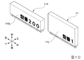
次に、本発明の変形例について説明する。図10は、変形例の基板の要部を拡大した斜
視図である。図10に示すように、本変形例では、図1に示す主要回路10に代えて、他
の主要回路110が基板部材2に搭載されているほかは、上記の実施形態と同様である。
図10では、複数の電子部品のうち、主要回路110及び第1出力回路11のみを示して
いる。
Next, a modification of the present invention will be described. FIG. 10 is an enlarged perspective view of a main part of the substrate of the modified example. As shown in FIG. 10, the present modification is the same as the above embodiment except that the
FIG. 10 shows only the
この変形例に係る主要回路110では、主要回路110の下面110Lに「型番200
」の文字が記載されている。このため、主要回路110における「型番200」の文字が
記載された下面110Lと、第1出力回路11における「型番1」の文字が記載された下
面11Lは、共通する方向を向いた面である。また、主要回路110における「型番20
0」の文字が表示された下面110Lは、主要回路110が実装された基板部材2の実装
面に直交する方向を向いた面である。また、図1に示す主要回路10では、その下面及び
上面から基板部材2の配線等に接続されるピン等が伸び出している。これに対して、主要
回路110では、その後面(基板部材2の実装面に対向する面)から、基板部材2の配線
等に接続されるピン等が伸び出している。
In the
"Is written. Therefore, the
The
このように、主要回路110の下面110Lに「型番200」の文字が記載されている
。第1出力回路11を一方向、具体的には斜め下方向(左斜め下方向または右斜め下方向
)からを同時に見た場合に、「型番200」の文字と第1出力回路11の下面11Lに記
載された「型番1」の文字を一気に視認することができる。したがって、基板部材2の実
装面の異なる方向を向いた面に「型番200」の文字が表示されていたとしても、主要回
路110が実装された基板1に正しい部品が取り付けられていることを容易に確認するこ
とができる。
As described above, the characters "model number 200" are written on the
また、主要回路110の下面110Lに「型番200」の文字が表示されていた場合、
第2出力回路12~第5出力回路15、及び第1入力回路21の前面12F~15F,2
1Fに表示された「型番2」「型番3」「型番4」「型番5」「型番3」の文字も「型番
200」の文字と一気に視認することができる。したがって、基板部材2の実装面に異な
る方向を向いた面に「型番200」の文字が表示されていたとしても、主要回路110の
基板1に正しい部品が取り付けられていることを容易に確認することができる。
Further, when the characters "model number 200" are displayed on the
Front 12F to 15F, 2 of the
The characters "
図11は、他の変形例の基板の要部を拡大した平面図である。図11に示す例において
は、出力回路の前面に表示された文字の向きが出力回路ごとに異なっている。具体的に、
主要回路210の前面に表示された「型番300」の文字は、読みやすい向きを向いてい
る。また、第1出力回路211に表示された「型番1」の文字は、第1出力回路211の
前面において読みやすい向きを向いている。第2出力回路212に表示された「型番2」
の文字は、第2出力回路212の前面において読みにくい向きを向いている。第3出力回
路213に表示された「型番3」の文字は、第3出力回路213の前面において読みやす
い向きを向いている。
FIG. 11 is an enlarged plan view of a main part of the substrate of another modified example. In the example shown in FIG. 11, the orientation of the characters displayed on the front surface of the output circuit is different for each output circuit. specifically,
The characters "model number 300" displayed on the front surface of the
Characters are oriented in a direction that is difficult to read on the front surface of the
この変形例では、主要回路210の前面に表示された「型番300」の文字、第1出力
回路211~第3出力回路213にそれぞれ表示された「型番1」~「型番3」の文字は
、読みやすい向きを向いていたり読みにくい向きを向いていたりして天地が不統一となっ
ている。しかしながら、これらの「型番300」「型番1」~「型番3」の文字は、いず
れも互いに向きが共通する主要回路210、第1出力回路211~第3出力回路213の
各前面に表示されている。このため、天地の向きは異なるものの、これらの文字を一気に
視認することができる。したがって、これらの電子部品が設けられた基板に正しい部品が
取り付けられていることを容易に確認することができる。
In this modification, the characters "model number 300" displayed on the front surface of the
図12は、他の変形例の基板の要部を拡大した平面である。図12においては、複数の
抵抗素子の整列の態様の変形例を示している。図12(A)に示す変形例では、同じ方向
を向いた第1抵抗素子31~第8抵抗素子38が千鳥に配置されており、第1抵抗素子3
1~第8抵抗素子38に描かれて第1カラーコードCC1となる第1ラインL1は、隣り
合う抵抗素子ごとに上下に段差を生じるようにして整列されている。第2ラインL2~第
4ラインL4についても、第1ラインL1と同様に、隣り合う抵抗素子ごとに上下に段差
を生じるようにして整列されている。このように、隣り合う抵抗素子同士が千鳥に配置さ
れ、第1ラインL1~第4ラインL4が上下に段差が生じるように整列された態様にして
、第1カラーコードCC1(第1ラインL1~第4ラインL4)の向きが共通するように
していもよい。
FIG. 12 is an enlarged flat surface of a main part of the substrate of another modified example. FIG. 12 shows a modified example of the mode of arranging a plurality of resistance elements. In the modified example shown in FIG. 12A, the
The first line L1 drawn on the first to
図12(B)に示す変形例では、同じ方向を向いた第1抵抗素子31~第5抵抗素子3
5が、その長手方向に連続するように配置されている。この変形例では、第1抵抗素子3
1~第5抵抗素子35のそれぞれにおける第1カラーコードCC1(第1ラインL1~第
4ラインL4)は、直線上等には配置されていないが、これらの向きは共通している。言
い換えると、第1ラインL1~第4ラインL4が一直線上に配置される場合には、複数の
抵抗素子がその第1ラインL1~第4ラインL4が延在する方向に沿って並設され、この
変形例では、複数の抵抗素子がその第1ラインL1~第4ラインL4が延在する方向に交
差(直交)する方向に沿って並設される。このように、複数の抵抗素子は、その第1ライ
ンL1~第4ラインL4が延在する方向に交差(直交)する方向に沿って並設されること
によって第1ラインL1~第4ラインL4の向きが共通するように設けられてもよい。要
は、複数の抵抗素子はバラバラではない態様で配置されていればよい。
In the modified example shown in FIG. 12B, the
5 are arranged so as to be continuous in the longitudinal direction thereof. In this modification, the
The first color code CC1 (first line L1 to fourth line L4) in each of the first to
なお、今回開示された実施の形態はすべての点で例示であって制限的なものではないと
考えられるべきである。本発明の範囲は上記した説明ではなく特許請求の範囲によって示
され、特許請求の範囲と均等の意味及び範囲内でのすべての変更が含まれることが意図さ
れる。
It should be noted that the embodiments disclosed this time are exemplary in all respects and are not restrictive. The scope of the present invention is shown by the scope of claims rather than the above description, and is intended to include all modifications within the meaning and scope equivalent to the scope of claims.
例えば、上記の実施形態では、基板1は、スロットマシンの筐体の奥方の板の手前側の
面に固定されるが、他の面、例えば、筐体の内左側の右面または内右側の左面に設けられ
てもよいし、スロットマシンにおけるリールユニットの上面に設けられていてもよい。ま
た、スロットマシンの前扉におけるリール窓が設けられた位置の上方に設けられていても
よい。また、基板の向きは、どの向きでもよく、上記の実施形態では、広い面(電子部品
の実装面)が前面を向くように配置されているが、当該広い面が上方向または下方向を向
くようにしてもよいし、左右いずれかの方向を向くようにしてもよい。また、前後上下左
右の各軸の少なくとも一軸に対して傾斜する角度で配置されてもよい。
For example, in the above embodiment, the
また、上記の例では、基板1は、遊技の制御を行う主要回路10を備えるいわゆる主基
板であるが、他の基板であってもよい。例えば、スロットマシンの演出を主に司る演出基
板であってもよいし、電源の供給に関する電源基板であってもよい。または、その他の基
板、例えば音声制御基板、ランプ制御基板、中継基板、払出制御基板、情報端子基板、発
射制御基板などであってもよい。また、上記の例では、基板1は、スロットマシンに設け
られた基板であるが、他の遊技機、例えばパチンコ遊技機(パチンコ機)に設けられた基
板であってもよい。
Further, in the above example, the
また、上記の例では、文字が記載された電子部品は回路素子、例えば集積回路であるが
、他の電子部品であってもよい。例えば、トランジスタ、抵抗、コンデンサなどの素子で
あってもよい。また、上記の例では、基板部材2における電子部品の実装面と共通する方
向を向いた面、またはその実装面に直交する面に文字が記載されているが、基板部材2に
おける電子部品の実装面と電子部品における文字が記載される面との関係は、他の関係と
なっていてもよい。例えば、基板部材2の実装面に対して、傾斜する面を有する電子部品
のその傾斜する面に文字が記載されていてもよいし、円筒状の電子部品の側面に文字が記
載されていてもよい。
Further, in the above example, the electronic component on which the characters are written is a circuit element, for example, an integrated circuit, but may be another electronic component. For example, it may be an element such as a transistor, a resistor, or a capacitor. Further, in the above example, the characters are written on the surface of the
また、上記の例では、電子部品を経由して入出力される信号は、第1入出力端子61、
第2入出力端子62、及び第3入出力端子63を介する以外には、基板1の外部に送信さ
れないが、これらの入出力端子を介することなく、外部との間で信号の入出力が行われる
ようにしてもよい。例えば、第1セグメント表示部51~第4セグメント表示部34に表
示される役比に関する信号を、基板1の外部に出力できるようにしてもよい。さらには、
基板1等のスロットマシン内の基板から出力される信号を、スロットマシンの外部の機器
に出力できるようにしてもよいし、基板1等のスロットマシン内の基板に外部から信号が
入力されるようにしてもよい。例えば、スロットマシンに関する情報を、ホールに設けら
れるデータ表示器等に出力できるようにしてもよい。
Further, in the above example, the signal input / output via the electronic component is the first input /
It is not transmitted to the outside of the
The signal output from the board in the slot machine such as the
また、上記の例では、基板部材2上においては、文字が記載されたすべての電子部品の
電子部品の近傍に文字が記載されているが、すべての電子部品のうちの一部の近傍にのみ
文字が記載されていてもよい。例えば、主要回路10の近傍にのみ文字が記載されていて
もよいし、出力回路の近傍にのみ文字が記載されていてもよい。また、基板部材2におけ
る上第1出力回路11Aの近傍位置に記載された文字は、上記の第1出力回路11Aの近
傍に記載された文字として説明した関連する文字であってもよい。
Further, in the above example, on the
また、電子部品との関係で基板部材2に記載される文字が異なっていてもよい。例えば
、出力回路の近傍には、出力回路に記載された文字と同一の文字が記載され、入力回路の
近傍には、入力回路に記載された文字と関連する文字が記載されるようにしてもよい。ま
た、1の電子部品、例えば出力回路の近傍では電子部品の上部に文字が記載され、他の電
子部品、例えば入力回路の近傍では電子部品の下部に文字が記載されていてもよい。
Further, the characters written on the
また、電子部品との関係で基板部材2に記載される文字の形状(フォント)、大きさ、
向きなどが異なるようにしてもよい。また、各電子部品に記載される文字についても、電
子部品ごとに記載される文字の形状(フォント)、大きさ、向きなどが異なるようにして
もよい。さらには、基板部材2上における電子部品の位置関係に応じて、基板部材2にお
ける電子部品の近傍に記載される文字や電子部品に記載される文字の形状(フォント)、
大きさ、向きなどが異なるようにしてもよい。
In addition, the shape (font) and size of the characters described on the
The orientation may be different. Further, the characters described in each electronic component may have different shapes (fonts), sizes, orientations, etc. of the characters described in each electronic component. Further, depending on the positional relationship of the electronic components on the
The size, orientation, etc. may be different.
(1)本発明の遊技機は、遊技を行う遊技機(例えば、スロットマシン、パチンコ遊技
機等)であって、複数種類の電子部品(例えば、主要回路、入力回路、出力回路、入出力
端子、抵抗、トランジスタ、コンデンサ等)が搭載された基板(例えば、基板1等)を備
え、前記複数種類の電子部品は、文字情報(例えば、上第1出力回路11A、中第1出力
回路11B、下第1出力回路11Cに記載された「型番1」の文字等)が記された複数の
特定電子部品(例えば、上第1出力回路11A、中第1出力回路11B、下第1出力回路
11C等)を含んでおり、前記複数の特定電子部品は、それぞれに記された前記文字情報
の向きが共通する(例えば、上第1出力回路11A、中第1出力回路11B、下第1出力
回路11Cに表示された「型番1」の文字は、いずれも読みやすい向きを向いている等)
ように前記基板に搭載されていることを特徴とする。
(1) The gaming machine of the present invention is a gaming machine (for example, a slot machine, a pachinko gaming machine, etc.) that plays a game, and is a plurality of types of electronic components (for example, a main circuit, an input circuit, an output circuit, an input / output terminal). , A substrate (for example,
As described above, it is characterized in that it is mounted on the substrate.
このような構成によれば、電子部品に記された文字情報に対して、一方向からの視認で
認識し易くできる。このため、基板に正しい部品取り付けられていることを容易に確認で
きる。
According to such a configuration, the character information written on the electronic component can be easily recognized visually from one direction. Therefore, it can be easily confirmed that the correct parts are mounted on the board.
(2)上記(1)に記載の遊技機において、前記複数種類の電子部品は、遊技の制御を
行う特別電子部品(例えば、主要回路10等)を含み、前記特別電子部品には、文字情報
が記されており(例えば、主要回路10に「型番100」の文字が記載されている等)、
複数の前記特定電子部品における前記文字情報の向き(例えば、第1出力回路11に記載
された「型番1」の文字の向き等)と、前記特別電子部品における前記文字の向き(例え
ば、主要回路10に記載された「型番100」の文字の向き等)が、いずれも特定の向き
となるように、複数の前記特定電子部品及び前記特別電子部品が前記基板に搭載されてい
るようにしてもよい。
(2) In the gaming machine according to (1) above, the plurality of types of electronic components include special electronic components (for example,
The orientation of the character information in the plurality of specific electronic components (for example, the orientation of the characters of "
このような構成によれば、特定電子部品とともに文字情報を認識し易くできる。 According to such a configuration, it is possible to easily recognize the character information together with the specific electronic component.
(3)上記(2)の遊技機において、前記基板に搭載され、文字情報が記された複数の
前記電子部品(例えば、主要回路10、第1出力回路11~第5出力回路15、第1入力
回路21)のうちの半数を超える前記電子部品(例えば、基板部材2に搭載された電子部
品であって文字が記載された電子部品のうちの主要回路10、上第1出力回路11A、中
第1出力回路11B、下第1出力回路11C、右第1入力回路21A、中第1入力回路2
1B、左第1入力回路21C等)は、それぞれに記された前記文字情報の面が前記特定の
向きとなる(例えば、主要回路10、上第1出力回路11A、中第1出力回路11B、下
第1出力回路11C、右第1入力回路21A、中第1入力回路21B、左第1入力回路2
1Cに記載された文字は、特定の向きを向いている等)ように前記基板に搭載されている
ようにしてもよい。
(3) In the game machine of the above (2), a plurality of the electronic components (for example, the
In 1B, the left
The characters described in 1C may be mounted on the substrate so as to face a specific direction, etc.).
このような構成によれば、他に設けられた電子部品とともに文字情報を認識し易くでき
る。
According to such a configuration, character information can be easily recognized together with other electronic components provided.
(4)上記(1)~(3)のいずれかの遊技機において、前記基板上における前記特定
電子部品の実装位置の近傍(例えば、第1出力回路11の近傍等)には、前記実装位置に
実装される前記特定電子部品と対応した文字情報(例えば、第1出力回路11に記載され
た「型番1」と同一の「型番1」の文字等)が記されており、前記基板上に記された文字
情報と、前記実装位置に実装された前記特定電子部品に記された文字情報の向きが共通す
る(例えば、第1出力回路11に記載された「型番1」と、基板部材2の記載された「型
番1」の文字の向きが、基板1を一方向から見たときに、その文字の下側が視点に近い側
に位置する等)ように、前記実装位置に実装された前記特定電子部品が前記基板に搭載さ
れているようにしてもよい。
(4) In any of the game machines (1) to (3), the mounting position is located near the mounting position of the specific electronic component on the substrate (for example, near the first output circuit 11). Character information corresponding to the specific electronic component mounted on the board (for example, the character of "
(5)本発明の遊技機は、遊技を行う遊技機(例えば、スロットマシン、パチンコ遊技
機等)であって、複数種類の電子部品(例えば、主要回路、入力回路、出力回路、入出力
端子、抵抗、トランジスタ、コンデンサ等)が搭載された基板(例えば、基板1等)を備
え、前記複数種類の電子部品は、複数の識別電子部品(例えば、第2出力回路12、第3
出力回路13、第4出力回路14、第5出力回路15、第1入力回路21等)を含み、前
記複数の識別電子部品は、第1種類の識別電子部品(例えば、出力回路として使用される
第3出力回路13等)と第2種類の識別電子部品(例えば、入力回路として使用される第
1入力回路21等)とを含んでおり、前記第1種類の識別電子部品と前記第2種類の識別
電子部品とは、外見から識別できるよう(第3出力回路13と第1入力回路21とは、外
見から識別できるように、前面に表示された「型番3」の文字の向きが異なり、互いに反
転させた関係となっている等)に、前記基板に搭載されていることを特徴とする。
(5) The gaming machine of the present invention is a gaming machine (for example, a slot machine, a pachinko gaming machine, etc.) that plays a game, and is a plurality of types of electronic components (for example, a main circuit, an input circuit, an output circuit, an input / output terminal). , A resistor, a transistor, a capacitor, etc.) are provided, and the plurality of types of electronic components include a plurality of identification electronic components (eg,
The plurality of identification electronic components include an
このような構成によれば、識別電子部品の態様によって、いずれの種類の識別電子部品
であるかを区別できる。このため、基板に正しい部品取り付けられていることを容易に確
認できる。
According to such a configuration, it is possible to distinguish which type of identification electronic component is according to the aspect of the identification electronic component. Therefore, it can be easily confirmed that the correct parts are mounted on the board.
(6)上記(5)に記載の遊技機において、前記第1種類の識別電子部品は、出力回路
に設けられた識別電子部品(例えば、第3出力回路13等)であり、前記第2種類の識別
電子部品は、入力回路に設けられた識別電子部品(例えば、第1入力回路21等)である
ようにしてもよい。
(6) In the gaming machine according to (5) above, the first type of identification electronic component is an identification electronic component (for example, a
このような構成によれば、信号の入力に用いられる電子部品と信号の出力に用いる電子
部品を容易に区別できる。
With such a configuration, it is possible to easily distinguish between the electronic component used for signal input and the electronic component used for signal output.
(7)上記(5)または(6)の遊技機において、前記複数種類の電子部品は、複数の
所定電子部品(例えば、第1出力回路11~第5出力回路15等)を含み、複数種類の所
定電子部品は、第1種類の第1所定電子部品(例えば、第2出力回路12等)を含み、前
記第1種類の識別電子部品と前記第1所定電子部品とは、同じ態様で前記基板に搭載され
ている(例えば、第2出力回路12と第3出力回路13は、いずれも読みにくい向きを向
く態様で基板1に搭載されている等)ようにしてもよい。
(7) In the gaming machine of the above (5) or (6), the plurality of types of electronic components include a plurality of predetermined electronic components (for example,
このような構成によれば、第1種類の電子部品を容易に区別できる。 With such a configuration, the first type of electronic component can be easily distinguished.
(8)上記(5)または(6)の遊技機において、前記複数種類の電子部品は、複数種
類の所定電子部品を含み(例えば、主要回路、入力回路、出力回路、入出力端子、抵抗、
トランジスタ、コンデンサの各電子部品は、第1出力回路11~第5出力回路15を含み
)、複数種類の所定電子部品は、第1種類の第1所定電子部品を含み(例えば、第1出力
回路11~第5出力回路15は、第2出力回路12を含み)、前記第1種類の識別電子部
品と前記第1所定電子部品とは、互いに近傍位置となるように前記基板に搭載されいてい
る(例えば、第3出力回路13と第2出力回路12とは、互いに近傍に配置されている等
)ようにしてもよい。
(8) In the gaming machine according to (5) or (6), the plurality of types of electronic components include a plurality of types of predetermined electronic components (for example, a main circuit, an input circuit, an output circuit, an input / output terminal, a resistor, and the like.
Each electronic component of the transistor and the capacitor includes the
このような構成によれば、第1種類の電子部品を容易に区別できる。 With such a configuration, the first type of electronic component can be easily distinguished.
(9)本発明の遊技機は、遊技を行う遊技機(例えば、スロットマシン、パチンコ遊技
機等)であって、複数種類の電子部品(例えば、主要回路、入力回路、出力回路、入出力
端子、抵抗、トランジスタ、コンデンサ等)が搭載された基板を備え、前記複数種類の電
子部品は、極性のない2つの端子(例えば、抵抗等)を備え、所定のマーク(例えば、第
1ラインL1~第4ラインL4からなる第1カラーコードCC1等)が付された複数の印
付電子部品(例えば、第1抵抗素子31~第8抵抗素子38等)と、複数の端子を有する
特殊電子部品(例えば、第1セグメント表示部51~第4セグメント表示部54等)を含
み、前記特殊電子部品における複数の端子には、それぞれ前記印付電子部品が接続されて
おり、前記特殊電子部品における複数の端子に接続された複数の前記印付電子部品は、前
記所定のマークの向きが共通する(例えば、第1抵抗素子31~第8抵抗素子38は、第
1ラインL1~第4ラインL4がそれぞれ一直線上に配置されるように並べられている等
)ように、前記基板に搭載されていることを特徴とする。
(9) The gaming machine of the present invention is a gaming machine (for example, a slot machine, a pachinko gaming machine, etc.) that plays a game, and is a plurality of types of electronic components (for example, a main circuit, an input circuit, an output circuit, an input / output terminal). , Resistors, transistors, capacitors, etc.), the plurality of types of electronic components are provided with two non-polar terminals (eg, resistors, etc.), and predetermined marks (eg, first line L1 to A plurality of marked electronic components (for example,
このような構成によれば、特殊電子部品に対して、印付電子部品が正しく接続されてい
ることを確認できる。したがって、基板に正しい部品取り付けられていることを容易に確
認できる遊技機を提供することである。
With such a configuration, it can be confirmed that the marked electronic component is correctly connected to the special electronic component. Therefore, it is an object of the present invention to provide a gaming machine that can easily confirm that the correct parts are attached to the board.
(10)上記(9)に記載の遊技機において、前記所定のマークは、前記印付電子部品
の性能を示す(例えば、第1カラーコードCC1は、第1抵抗素子31~第8抵抗素子3
8の抵抗値及び許容差を示す等)ようにしてもよい。
(10) In the gaming machine according to (9) above, the predetermined mark indicates the performance of the marked electronic component (for example, the first color code CC1 is the
The resistance value and tolerance of 8 may be shown).
このような構成によれば、正しい性能の印付電子部品であるかを容易に確認できる。 With such a configuration, it is possible to easily confirm whether the electronic component is marked with the correct performance.
(11)上記(9)または(10)の遊技機において、前記印付電子部品は整列して前
記基板に搭載されているようにしてもよい。
(11) In the gaming machine of (9) or (10), the marked electronic components may be aligned and mounted on the substrate.
このような構成によれば、互いのマークの比較を行い易くできる。 With such a configuration, it is possible to easily compare the marks with each other.
(12)上記(9)~(11)のうちのいずれかの遊技機において、前記印付電子部品
は、複数の第1印付電子部品(例えば、第1抵抗素子31~第8抵抗素子38等)と、前
記第1印付電子部品と同種かつ異性能の第2印付電子部品(例えば、異性能抵抗素子41
等)と含み、前記複数種類の電子部品は、所定端子を有する第2特殊電子部品(例えば、
電源確認ランプ55等)を含み、前記第2特殊電子部品における前記所定端子に、前記第
2印付電子部品が接続されており(例えば、電源確認ランプ55に異性能抵抗素子41が
接続されている等)、前記第2印付電子部品は、整列された前記複数の第1印付電子部品
と並んで所定のマークが同じ向きとなるように前記基板に搭載されている(例えば、異性
能抵抗素子41の第2カラーコードCC2の第5ラインL5~第8ラインL8は、第1抵
抗素子31~第8抵抗素子38の第1カラーコードCC1の第1ラインL1~第4ライン
L4と一直線上に配置されるように並べられている等)ようにしてもよい。
(12) In any of the game machines (9) to (11) above, the marked electronic component is a plurality of first marked electronic components (for example,
The plurality of types of electronic components include, for example, a second special electronic component having a predetermined terminal (for example,
The second marked electronic component is connected to the predetermined terminal of the second special electronic component including the power supply confirmation lamp 55 (for example, the different
このような構成によれば、用途の異なる部品間で、互いのマークの比較を行い易くでき
る。
With such a configuration, it is possible to easily compare marks with each other among parts having different uses.
(13)上記(9)~(12)のうちのいずれかの遊技機において、前記特殊電子部品
のうちの少なくとも一つは、遊技機の性能表示に用いられる性能表示手段(例えば、第1
セグメント表示部51~第4セグメント表示部54は、遊技機の役比を表示する役比表示
手段である等)を備えるようにしてもよい。
(13) In any of the above (9) to (12), at least one of the special electronic components is a performance display means (for example, first) used for displaying the performance of the game machine.
The
このような構成によれば、遊技機の性能表示にあたって正常な部品が取り付けられてい
るかを表示できる。
With such a configuration, it is possible to display whether or not normal parts are attached when displaying the performance of the gaming machine.
1…基板
2…基板部材
10…主要回路
11…第1出力回路
12…第2出力回路
13…第3出力回路
14…第4出力回路
15…第5出力回路
21…第1入力回路
31~38…抵抗素子
41…異性能抵抗素子
51~54…セグメント表示部
55…電源確認ランプ
1 ...
Claims (1)
複数種類の電子部品が搭載された基板を備え、
前記複数種類の電子部品は、
文字情報が記された特定電子部品と、
極性のない2つの端子を備え、所定のマークが付された複数の印付電子部品と、
複数の端子を有する特殊電子部品と、
所定電子部品と、を含み、
前記特殊電子部品における複数の端子には、それぞれ前記複数の印付電子部品のうちの複数の特殊印付電子部品が接続されており、
前記所定電子部品には、前記複数の印付電子部品のうちの所定印付電子部品が接続されており、
前記特殊電子部品における複数の端子に接続された前記複数の特殊印付電子部品は、前記所定のマークの向きが共通するように、前記基板に並んで搭載されているとともに、
前記所定電子部品に接続された前記所定印付電子部品は、前記特殊電子部品における複数の端子に接続された前記複数の特殊印付電子部品と並んで、前記特殊電子部品における複数の端子に接続された前記複数の特殊印付電子部品と前記所定のマークの向きが共通するように、前記基板に搭載されており、
前記特定電子部品は、前記基板に対し垂直に起立するように搭載され、
前記特定電子部品に記された文字情報は、前記特定電子部品の一面に記されており、
前記基板上における前記特定電子部品の実装位置の近傍には、前記実装位置に実装される前記特定電子部品と対応した文字情報が記されており、
前記基板上に記された前記特定電子部品と対応した文字情報は、前記実装位置に実装された前記特定電子部品の文字情報が記された一面側の近傍に記されている、遊技機。 It is a gaming machine that plays games,
Equipped with a board on which multiple types of electronic components are mounted,
The plurality of types of electronic components are
Specific electronic components with textual information and
Multiple marked electronic components with two non-polar terminals, marked with a given mark, and
Special electronic components with multiple terminals and
Including certain electronic components,
A plurality of specially marked electronic components among the plurality of marked electronic components are connected to the plurality of terminals of the special electronic component.
A predetermined marked electronic component among the plurality of marked electronic components is connected to the predetermined electronic component.
The plurality of specially marked electronic components connected to the plurality of terminals of the special electronic component are mounted side by side on the substrate so that the orientation of the predetermined mark is common.
The predetermined marked electronic component connected to the predetermined electronic component is connected to a plurality of terminals in the special electronic component along with the plurality of specially marked electronic components connected to the plurality of terminals in the special electronic component. It is mounted on the substrate so that the orientation of the predetermined mark is the same as that of the plurality of specially marked electronic components.
The specific electronic component is mounted so as to stand upright with respect to the substrate.
The character information written on the specific electronic component is written on one side of the specific electronic component.
In the vicinity of the mounting position of the specific electronic component on the substrate, character information corresponding to the specific electronic component mounted at the mounting position is written.
The character information corresponding to the specific electronic component written on the substrate is written in the vicinity of one side on which the character information of the specific electronic component mounted at the mounting position is written.
Priority Applications (1)
| Application Number | Priority Date | Filing Date | Title |
|---|---|---|---|
| JP2018074757A JP7068901B2 (en) | 2018-04-09 | 2018-04-09 | Pachinko machine |
Applications Claiming Priority (1)
| Application Number | Priority Date | Filing Date | Title |
|---|---|---|---|
| JP2018074757A JP7068901B2 (en) | 2018-04-09 | 2018-04-09 | Pachinko machine |
Publications (3)
| Publication Number | Publication Date |
|---|---|
| JP2019180767A JP2019180767A (en) | 2019-10-24 |
| JP2019180767A5 JP2019180767A5 (en) | 2021-08-26 |
| JP7068901B2 true JP7068901B2 (en) | 2022-05-17 |
Family
ID=68337380
Family Applications (1)
| Application Number | Title | Priority Date | Filing Date |
|---|---|---|---|
| JP2018074757A Active JP7068901B2 (en) | 2018-04-09 | 2018-04-09 | Pachinko machine |
Country Status (1)
| Country | Link |
|---|---|
| JP (1) | JP7068901B2 (en) |
Citations (4)
| Publication number | Priority date | Publication date | Assignee | Title |
|---|---|---|---|---|
| JP2005087623A (en) | 2003-09-19 | 2005-04-07 | Samii Kk | Label and game machine |
| JP2006100716A (en) | 2004-09-30 | 2006-04-13 | Orion Denki Kk | Electronic appliance having indicated attaching sense of electronic component |
| JP2010012058A (en) | 2008-07-04 | 2010-01-21 | Daito Giken:Kk | Game machine |
| JP2017225754A (en) | 2016-06-24 | 2017-12-28 | 山佐株式会社 | Game machine |
-
2018
- 2018-04-09 JP JP2018074757A patent/JP7068901B2/en active Active
Patent Citations (4)
| Publication number | Priority date | Publication date | Assignee | Title |
|---|---|---|---|---|
| JP2005087623A (en) | 2003-09-19 | 2005-04-07 | Samii Kk | Label and game machine |
| JP2006100716A (en) | 2004-09-30 | 2006-04-13 | Orion Denki Kk | Electronic appliance having indicated attaching sense of electronic component |
| JP2010012058A (en) | 2008-07-04 | 2010-01-21 | Daito Giken:Kk | Game machine |
| JP2017225754A (en) | 2016-06-24 | 2017-12-28 | 山佐株式会社 | Game machine |
Also Published As
| Publication number | Publication date |
|---|---|
| JP2019180767A (en) | 2019-10-24 |
Similar Documents
| Publication | Publication Date | Title |
|---|---|---|
| JP7019495B2 (en) | Pachinko machine | |
| JP6974227B2 (en) | Pachinko machine | |
| JP6810081B2 (en) | Game machine | |
| JP6648068B2 (en) | Gaming machine | |
| JP2006068252A (en) | Game machine | |
| JP6822681B2 (en) | Game machine | |
| JP6822680B2 (en) | Game machine | |
| JP7068900B2 (en) | Pachinko machine | |
| JP6974228B2 (en) | Pachinko machine | |
| JP6889480B2 (en) | Pachinko machine | |
| JP7068901B2 (en) | Pachinko machine | |
| JP6896289B2 (en) | Pachinko machine | |
| JP6844860B2 (en) | Game machine | |
| JP6889482B2 (en) | Pachinko machine | |
| JP6896287B2 (en) | Pachinko machine | |
| JP7081812B2 (en) | Pachinko machine | |
| JP6954635B2 (en) | Pachinko machine | |
| JP6889481B2 (en) | Pachinko machine | |
| JP6844863B2 (en) | Game machine | |
| JP6502867B2 (en) | Gaming machine | |
| JP6502866B2 (en) | Gaming machine | |
| JP2020044051A (en) | Game machine | |
| JP6954634B2 (en) | Pachinko machine | |
| JP6867041B2 (en) | Pachinko machine | |
| JP6867039B2 (en) | Pachinko machine |
Legal Events
| Date | Code | Title | Description |
|---|---|---|---|
| A621 | Written request for application examination |
Free format text: JAPANESE INTERMEDIATE CODE: A621 Effective date: 20210312 |
|
| A521 | Request for written amendment filed |
Free format text: JAPANESE INTERMEDIATE CODE: A523 Effective date: 20210716 |
|
| A977 | Report on retrieval |
Free format text: JAPANESE INTERMEDIATE CODE: A971007 Effective date: 20220126 |
|
| A131 | Notification of reasons for refusal |
Free format text: JAPANESE INTERMEDIATE CODE: A131 Effective date: 20220201 |
|
| A521 | Request for written amendment filed |
Free format text: JAPANESE INTERMEDIATE CODE: A523 Effective date: 20220328 |
|
| TRDD | Decision of grant or rejection written | ||
| A01 | Written decision to grant a patent or to grant a registration (utility model) |
Free format text: JAPANESE INTERMEDIATE CODE: A01 Effective date: 20220426 |
|
| A61 | First payment of annual fees (during grant procedure) |
Free format text: JAPANESE INTERMEDIATE CODE: A61 Effective date: 20220502 |
|
| R150 | Certificate of patent or registration of utility model |
Ref document number: 7068901 Country of ref document: JP Free format text: JAPANESE INTERMEDIATE CODE: R150 |