JP2005514765A - エッチング停止層としてポリシリコン再酸化層を使用することによって、シリコン層の凹部を減少する窒化オフセットスペーサ - Google Patents
エッチング停止層としてポリシリコン再酸化層を使用することによって、シリコン層の凹部を減少する窒化オフセットスペーサ Download PDFInfo
- Publication number
- JP2005514765A JP2005514765A JP2003555572A JP2003555572A JP2005514765A JP 2005514765 A JP2005514765 A JP 2005514765A JP 2003555572 A JP2003555572 A JP 2003555572A JP 2003555572 A JP2003555572 A JP 2003555572A JP 2005514765 A JP2005514765 A JP 2005514765A
- Authority
- JP
- Japan
- Prior art keywords
- layer
- substrate
- forming
- polysilicon
- nitride
- Prior art date
- Legal status (The legal status is an assumption and is not a legal conclusion. Google has not performed a legal analysis and makes no representation as to the accuracy of the status listed.)
- Pending
Links
- 229910021420 polycrystalline silicon Inorganic materials 0.000 title claims abstract description 63
- 229920005591 polysilicon Polymers 0.000 title claims abstract description 63
- 238000010405 reoxidation reaction Methods 0.000 title claims abstract description 46
- 150000004767 nitrides Chemical class 0.000 title claims abstract description 39
- 125000006850 spacer group Chemical group 0.000 title claims abstract description 36
- XUIMIQQOPSSXEZ-UHFFFAOYSA-N Silicon Chemical compound [Si] XUIMIQQOPSSXEZ-UHFFFAOYSA-N 0.000 title abstract description 15
- 229910052710 silicon Inorganic materials 0.000 title abstract description 15
- 239000010703 silicon Substances 0.000 title abstract description 15
- 239000000758 substrate Substances 0.000 claims abstract description 51
- 238000000034 method Methods 0.000 claims abstract description 31
- 239000004065 semiconductor Substances 0.000 claims abstract description 18
- 239000007943 implant Substances 0.000 claims description 31
- 238000005530 etching Methods 0.000 claims description 28
- 125000001475 halogen functional group Chemical group 0.000 claims description 22
- 238000000151 deposition Methods 0.000 claims description 5
- 238000010438 heat treatment Methods 0.000 claims description 2
- 238000001020 plasma etching Methods 0.000 claims description 2
- 230000015572 biosynthetic process Effects 0.000 description 11
- 230000008569 process Effects 0.000 description 10
- 239000012535 impurity Substances 0.000 description 6
- 229910052796 boron Inorganic materials 0.000 description 4
- 238000009792 diffusion process Methods 0.000 description 4
- 230000000694 effects Effects 0.000 description 4
- 238000004519 manufacturing process Methods 0.000 description 4
- 230000035515 penetration Effects 0.000 description 4
- ZOXJGFHDIHLPTG-UHFFFAOYSA-N Boron Chemical compound [B] ZOXJGFHDIHLPTG-UHFFFAOYSA-N 0.000 description 3
- 230000008901 benefit Effects 0.000 description 3
- 238000004518 low pressure chemical vapour deposition Methods 0.000 description 3
- 229910052581 Si3N4 Inorganic materials 0.000 description 2
- 230000004888 barrier function Effects 0.000 description 2
- 230000015556 catabolic process Effects 0.000 description 2
- 230000008021 deposition Effects 0.000 description 2
- 238000005553 drilling Methods 0.000 description 2
- 238000001312 dry etching Methods 0.000 description 2
- 238000005516 engineering process Methods 0.000 description 2
- 239000002184 metal Substances 0.000 description 2
- 238000000623 plasma-assisted chemical vapour deposition Methods 0.000 description 2
- 230000009467 reduction Effects 0.000 description 2
- HQVNEWCFYHHQES-UHFFFAOYSA-N silicon nitride Chemical compound N12[Si]34N5[Si]62N3[Si]51N64 HQVNEWCFYHHQES-UHFFFAOYSA-N 0.000 description 2
- VYPSYNLAJGMNEJ-UHFFFAOYSA-N Silicium dioxide Chemical compound O=[Si]=O VYPSYNLAJGMNEJ-UHFFFAOYSA-N 0.000 description 1
- 230000004913 activation Effects 0.000 description 1
- 230000002411 adverse Effects 0.000 description 1
- 238000000137 annealing Methods 0.000 description 1
- 150000001638 boron Chemical class 0.000 description 1
- 238000007796 conventional method Methods 0.000 description 1
- 230000007423 decrease Effects 0.000 description 1
- 230000001066 destructive effect Effects 0.000 description 1
- 239000007772 electrode material Substances 0.000 description 1
- 230000003628 erosive effect Effects 0.000 description 1
- 230000005669 field effect Effects 0.000 description 1
- 238000002513 implantation Methods 0.000 description 1
- 239000011810 insulating material Substances 0.000 description 1
- 239000000463 material Substances 0.000 description 1
- 230000002265 prevention Effects 0.000 description 1
- 229910052814 silicon oxide Inorganic materials 0.000 description 1
- 238000001039 wet etching Methods 0.000 description 1
Images


Classifications
-
- H—ELECTRICITY
- H01—ELECTRIC ELEMENTS
- H01L—SEMICONDUCTOR DEVICES NOT COVERED BY CLASS H10
- H01L21/00—Processes or apparatus adapted for the manufacture or treatment of semiconductor or solid state devices or of parts thereof
- H01L21/02—Manufacture or treatment of semiconductor devices or of parts thereof
- H01L21/04—Manufacture or treatment of semiconductor devices or of parts thereof the devices having potential barriers, e.g. a PN junction, depletion layer or carrier concentration layer
- H01L21/18—Manufacture or treatment of semiconductor devices or of parts thereof the devices having potential barriers, e.g. a PN junction, depletion layer or carrier concentration layer the devices having semiconductor bodies comprising elements of Group IV of the Periodic Table or AIIIBV compounds with or without impurities, e.g. doping materials
- H01L21/28—Manufacture of electrodes on semiconductor bodies using processes or apparatus not provided for in groups H01L21/20 - H01L21/268
- H01L21/28008—Making conductor-insulator-semiconductor electrodes
- H01L21/28017—Making conductor-insulator-semiconductor electrodes the insulator being formed after the semiconductor body, the semiconductor being silicon
- H01L21/28247—Making conductor-insulator-semiconductor electrodes the insulator being formed after the semiconductor body, the semiconductor being silicon passivation or protection of the electrode, e.g. using re-oxidation
-
- H—ELECTRICITY
- H01—ELECTRIC ELEMENTS
- H01L—SEMICONDUCTOR DEVICES NOT COVERED BY CLASS H10
- H01L21/00—Processes or apparatus adapted for the manufacture or treatment of semiconductor or solid state devices or of parts thereof
- H01L21/02—Manufacture or treatment of semiconductor devices or of parts thereof
- H01L21/04—Manufacture or treatment of semiconductor devices or of parts thereof the devices having potential barriers, e.g. a PN junction, depletion layer or carrier concentration layer
- H01L21/18—Manufacture or treatment of semiconductor devices or of parts thereof the devices having potential barriers, e.g. a PN junction, depletion layer or carrier concentration layer the devices having semiconductor bodies comprising elements of Group IV of the Periodic Table or AIIIBV compounds with or without impurities, e.g. doping materials
- H01L21/30—Treatment of semiconductor bodies using processes or apparatus not provided for in groups H01L21/20 - H01L21/26
- H01L21/31—Treatment of semiconductor bodies using processes or apparatus not provided for in groups H01L21/20 - H01L21/26 to form insulating layers thereon, e.g. for masking or by using photolithographic techniques; After treatment of these layers; Selection of materials for these layers
-
- H—ELECTRICITY
- H01—ELECTRIC ELEMENTS
- H01L—SEMICONDUCTOR DEVICES NOT COVERED BY CLASS H10
- H01L21/00—Processes or apparatus adapted for the manufacture or treatment of semiconductor or solid state devices or of parts thereof
- H01L21/02—Manufacture or treatment of semiconductor devices or of parts thereof
- H01L21/02104—Forming layers
- H01L21/02107—Forming insulating materials on a substrate
- H01L21/02109—Forming insulating materials on a substrate characterised by the type of layer, e.g. type of material, porous/non-porous, pre-cursors, mixtures or laminates
- H01L21/02112—Forming insulating materials on a substrate characterised by the type of layer, e.g. type of material, porous/non-porous, pre-cursors, mixtures or laminates characterised by the material of the layer
- H01L21/02123—Forming insulating materials on a substrate characterised by the type of layer, e.g. type of material, porous/non-porous, pre-cursors, mixtures or laminates characterised by the material of the layer the material containing silicon
- H01L21/02164—Forming insulating materials on a substrate characterised by the type of layer, e.g. type of material, porous/non-porous, pre-cursors, mixtures or laminates characterised by the material of the layer the material containing silicon the material being a silicon oxide, e.g. SiO2
-
- H—ELECTRICITY
- H01—ELECTRIC ELEMENTS
- H01L—SEMICONDUCTOR DEVICES NOT COVERED BY CLASS H10
- H01L21/00—Processes or apparatus adapted for the manufacture or treatment of semiconductor or solid state devices or of parts thereof
- H01L21/02—Manufacture or treatment of semiconductor devices or of parts thereof
- H01L21/02104—Forming layers
- H01L21/02107—Forming insulating materials on a substrate
- H01L21/02109—Forming insulating materials on a substrate characterised by the type of layer, e.g. type of material, porous/non-porous, pre-cursors, mixtures or laminates
- H01L21/02112—Forming insulating materials on a substrate characterised by the type of layer, e.g. type of material, porous/non-porous, pre-cursors, mixtures or laminates characterised by the material of the layer
- H01L21/02123—Forming insulating materials on a substrate characterised by the type of layer, e.g. type of material, porous/non-porous, pre-cursors, mixtures or laminates characterised by the material of the layer the material containing silicon
- H01L21/0217—Forming insulating materials on a substrate characterised by the type of layer, e.g. type of material, porous/non-porous, pre-cursors, mixtures or laminates characterised by the material of the layer the material containing silicon the material being a silicon nitride not containing oxygen, e.g. SixNy or SixByNz
-
- H—ELECTRICITY
- H01—ELECTRIC ELEMENTS
- H01L—SEMICONDUCTOR DEVICES NOT COVERED BY CLASS H10
- H01L21/00—Processes or apparatus adapted for the manufacture or treatment of semiconductor or solid state devices or of parts thereof
- H01L21/02—Manufacture or treatment of semiconductor devices or of parts thereof
- H01L21/02104—Forming layers
- H01L21/02107—Forming insulating materials on a substrate
- H01L21/02109—Forming insulating materials on a substrate characterised by the type of layer, e.g. type of material, porous/non-porous, pre-cursors, mixtures or laminates
- H01L21/022—Forming insulating materials on a substrate characterised by the type of layer, e.g. type of material, porous/non-porous, pre-cursors, mixtures or laminates the layer being a laminate, i.e. composed of sublayers, e.g. stacks of alternating high-k metal oxides
-
- H—ELECTRICITY
- H01—ELECTRIC ELEMENTS
- H01L—SEMICONDUCTOR DEVICES NOT COVERED BY CLASS H10
- H01L21/00—Processes or apparatus adapted for the manufacture or treatment of semiconductor or solid state devices or of parts thereof
- H01L21/02—Manufacture or treatment of semiconductor devices or of parts thereof
- H01L21/02104—Forming layers
- H01L21/02107—Forming insulating materials on a substrate
- H01L21/02225—Forming insulating materials on a substrate characterised by the process for the formation of the insulating layer
- H01L21/02227—Forming insulating materials on a substrate characterised by the process for the formation of the insulating layer formation by a process other than a deposition process
- H01L21/0223—Forming insulating materials on a substrate characterised by the process for the formation of the insulating layer formation by a process other than a deposition process formation by oxidation, e.g. oxidation of the substrate
- H01L21/02233—Forming insulating materials on a substrate characterised by the process for the formation of the insulating layer formation by a process other than a deposition process formation by oxidation, e.g. oxidation of the substrate of the semiconductor substrate or a semiconductor layer
- H01L21/02236—Forming insulating materials on a substrate characterised by the process for the formation of the insulating layer formation by a process other than a deposition process formation by oxidation, e.g. oxidation of the substrate of the semiconductor substrate or a semiconductor layer group IV semiconductor
- H01L21/02238—Forming insulating materials on a substrate characterised by the process for the formation of the insulating layer formation by a process other than a deposition process formation by oxidation, e.g. oxidation of the substrate of the semiconductor substrate or a semiconductor layer group IV semiconductor silicon in uncombined form, i.e. pure silicon
-
- H—ELECTRICITY
- H01—ELECTRIC ELEMENTS
- H01L—SEMICONDUCTOR DEVICES NOT COVERED BY CLASS H10
- H01L21/00—Processes or apparatus adapted for the manufacture or treatment of semiconductor or solid state devices or of parts thereof
- H01L21/02—Manufacture or treatment of semiconductor devices or of parts thereof
- H01L21/02104—Forming layers
- H01L21/02107—Forming insulating materials on a substrate
- H01L21/02225—Forming insulating materials on a substrate characterised by the process for the formation of the insulating layer
- H01L21/02227—Forming insulating materials on a substrate characterised by the process for the formation of the insulating layer formation by a process other than a deposition process
- H01L21/02255—Forming insulating materials on a substrate characterised by the process for the formation of the insulating layer formation by a process other than a deposition process formation by thermal treatment
-
- H—ELECTRICITY
- H01—ELECTRIC ELEMENTS
- H01L—SEMICONDUCTOR DEVICES NOT COVERED BY CLASS H10
- H01L21/00—Processes or apparatus adapted for the manufacture or treatment of semiconductor or solid state devices or of parts thereof
- H01L21/02—Manufacture or treatment of semiconductor devices or of parts thereof
- H01L21/02104—Forming layers
- H01L21/02107—Forming insulating materials on a substrate
- H01L21/02225—Forming insulating materials on a substrate characterised by the process for the formation of the insulating layer
- H01L21/0226—Forming insulating materials on a substrate characterised by the process for the formation of the insulating layer formation by a deposition process
- H01L21/02263—Forming insulating materials on a substrate characterised by the process for the formation of the insulating layer formation by a deposition process deposition from the gas or vapour phase
- H01L21/02271—Forming insulating materials on a substrate characterised by the process for the formation of the insulating layer formation by a deposition process deposition from the gas or vapour phase deposition by decomposition or reaction of gaseous or vapour phase compounds, i.e. chemical vapour deposition
- H01L21/02274—Forming insulating materials on a substrate characterised by the process for the formation of the insulating layer formation by a deposition process deposition from the gas or vapour phase deposition by decomposition or reaction of gaseous or vapour phase compounds, i.e. chemical vapour deposition in the presence of a plasma [PECVD]
-
- H—ELECTRICITY
- H01—ELECTRIC ELEMENTS
- H01L—SEMICONDUCTOR DEVICES NOT COVERED BY CLASS H10
- H01L21/00—Processes or apparatus adapted for the manufacture or treatment of semiconductor or solid state devices or of parts thereof
- H01L21/02—Manufacture or treatment of semiconductor devices or of parts thereof
- H01L21/04—Manufacture or treatment of semiconductor devices or of parts thereof the devices having potential barriers, e.g. a PN junction, depletion layer or carrier concentration layer
- H01L21/18—Manufacture or treatment of semiconductor devices or of parts thereof the devices having potential barriers, e.g. a PN junction, depletion layer or carrier concentration layer the devices having semiconductor bodies comprising elements of Group IV of the Periodic Table or AIIIBV compounds with or without impurities, e.g. doping materials
- H01L21/30—Treatment of semiconductor bodies using processes or apparatus not provided for in groups H01L21/20 - H01L21/26
- H01L21/31—Treatment of semiconductor bodies using processes or apparatus not provided for in groups H01L21/20 - H01L21/26 to form insulating layers thereon, e.g. for masking or by using photolithographic techniques; After treatment of these layers; Selection of materials for these layers
- H01L21/3105—After-treatment
- H01L21/311—Etching the insulating layers by chemical or physical means
- H01L21/31105—Etching inorganic layers
- H01L21/31111—Etching inorganic layers by chemical means
- H01L21/31116—Etching inorganic layers by chemical means by dry-etching
-
- H—ELECTRICITY
- H01—ELECTRIC ELEMENTS
- H01L—SEMICONDUCTOR DEVICES NOT COVERED BY CLASS H10
- H01L29/00—Semiconductor devices specially adapted for rectifying, amplifying, oscillating or switching and having potential barriers; Capacitors or resistors having potential barriers, e.g. a PN-junction depletion layer or carrier concentration layer; Details of semiconductor bodies or of electrodes thereof ; Multistep manufacturing processes therefor
- H01L29/66—Types of semiconductor device ; Multistep manufacturing processes therefor
- H01L29/66007—Multistep manufacturing processes
- H01L29/66075—Multistep manufacturing processes of devices having semiconductor bodies comprising group 14 or group 13/15 materials
- H01L29/66227—Multistep manufacturing processes of devices having semiconductor bodies comprising group 14 or group 13/15 materials the devices being controllable only by the electric current supplied or the electric potential applied, to an electrode which does not carry the current to be rectified, amplified or switched, e.g. three-terminal devices
- H01L29/66409—Unipolar field-effect transistors
- H01L29/66477—Unipolar field-effect transistors with an insulated gate, i.e. MISFET
- H01L29/6656—Unipolar field-effect transistors with an insulated gate, i.e. MISFET using multiple spacer layers, e.g. multiple sidewall spacers
-
- H—ELECTRICITY
- H01—ELECTRIC ELEMENTS
- H01L—SEMICONDUCTOR DEVICES NOT COVERED BY CLASS H10
- H01L29/00—Semiconductor devices specially adapted for rectifying, amplifying, oscillating or switching and having potential barriers; Capacitors or resistors having potential barriers, e.g. a PN-junction depletion layer or carrier concentration layer; Details of semiconductor bodies or of electrodes thereof ; Multistep manufacturing processes therefor
- H01L29/66—Types of semiconductor device ; Multistep manufacturing processes therefor
- H01L29/66007—Multistep manufacturing processes
- H01L29/66075—Multistep manufacturing processes of devices having semiconductor bodies comprising group 14 or group 13/15 materials
- H01L29/66227—Multistep manufacturing processes of devices having semiconductor bodies comprising group 14 or group 13/15 materials the devices being controllable only by the electric current supplied or the electric potential applied, to an electrode which does not carry the current to be rectified, amplified or switched, e.g. three-terminal devices
- H01L29/66409—Unipolar field-effect transistors
- H01L29/66477—Unipolar field-effect transistors with an insulated gate, i.e. MISFET
- H01L29/66568—Lateral single gate silicon transistors
- H01L29/66575—Lateral single gate silicon transistors where the source and drain or source and drain extensions are self-aligned to the sides of the gate
- H01L29/6659—Lateral single gate silicon transistors where the source and drain or source and drain extensions are self-aligned to the sides of the gate with both lightly doped source and drain extensions and source and drain self-aligned to the sides of the gate, e.g. lightly doped drain [LDD] MOSFET, double diffused drain [DDD] MOSFET
-
- H—ELECTRICITY
- H01—ELECTRIC ELEMENTS
- H01L—SEMICONDUCTOR DEVICES NOT COVERED BY CLASS H10
- H01L21/00—Processes or apparatus adapted for the manufacture or treatment of semiconductor or solid state devices or of parts thereof
- H01L21/02—Manufacture or treatment of semiconductor devices or of parts thereof
- H01L21/04—Manufacture or treatment of semiconductor devices or of parts thereof the devices having potential barriers, e.g. a PN junction, depletion layer or carrier concentration layer
- H01L21/18—Manufacture or treatment of semiconductor devices or of parts thereof the devices having potential barriers, e.g. a PN junction, depletion layer or carrier concentration layer the devices having semiconductor bodies comprising elements of Group IV of the Periodic Table or AIIIBV compounds with or without impurities, e.g. doping materials
- H01L21/30—Treatment of semiconductor bodies using processes or apparatus not provided for in groups H01L21/20 - H01L21/26
- H01L21/31—Treatment of semiconductor bodies using processes or apparatus not provided for in groups H01L21/20 - H01L21/26 to form insulating layers thereon, e.g. for masking or by using photolithographic techniques; After treatment of these layers; Selection of materials for these layers
- H01L21/314—Inorganic layers
- H01L21/318—Inorganic layers composed of nitrides
- H01L21/3185—Inorganic layers composed of nitrides of siliconnitrides
Landscapes
- Engineering & Computer Science (AREA)
- Power Engineering (AREA)
- Microelectronics & Electronic Packaging (AREA)
- Physics & Mathematics (AREA)
- Manufacturing & Machinery (AREA)
- Condensed Matter Physics & Semiconductors (AREA)
- General Physics & Mathematics (AREA)
- Computer Hardware Design (AREA)
- Chemical & Material Sciences (AREA)
- Chemical Kinetics & Catalysis (AREA)
- Ceramic Engineering (AREA)
- Plasma & Fusion (AREA)
- Inorganic Chemistry (AREA)
- General Chemical & Material Sciences (AREA)
- Insulated Gate Type Field-Effect Transistor (AREA)
- Electrodes Of Semiconductors (AREA)
- Drying Of Semiconductors (AREA)
Abstract
Description
電界効果トランジスタ(FET)についてのソース/ドレイン領域間の間隔の減少によって、パンチスルー現象、ソース・ドレイン間の降伏電圧の減少、しきい値電圧(Vt)の減少、Sファクタ(subthreshold swing)の増加のような短チャネル効果が生じる。
この短チャネル効果を抑制するために、半導体産業は、常にMOSFETデバイスについての製造プロセスを最適化している。
浅い接合は、ソース/ドレイン空乏領域のチャネルへの浸食を少なくするので、CMOSデバイスのVLSI製造における最近の動向は、ソース/ドレイン領域の接合深さを浅くする方向に向かっている。
これらのサイズでは、実効チャネル長が少しでも減少すると、トランジスタの降伏電圧を低下させる観点でコストがかかる可能性がある。
従って、ソース/ドレイン中の不純物の横方向の拡散の制限はますます重要である。
ハロー・インプラントの不純物は、ソースおよびドレインの導電型(conductivity type )と反対の導電型を有する。
通常、ハロー・インプラントは、ゲートを定義した後であってソース/ドレイン拡散の前に行われる。
マスク効果により、ハロー・インプラントは、典型的にソース/ドレイン領域近傍において最も高い不純物濃度を示す。
ソース/ドレイン中の不純物の垂直方向の拡散を防止するために、ハロー・インプラントのためのインプラント・エネルギーは、不純物濃度の最も高い位置から離れた位置のハローの深さがソース/ドレインのインプラントの深さよりも深くなるように、慎重に選択されるべきである。
ハローを形成し、その後ゲート電極のサイドウォール上のオフセット・スペーサを形成し、それからソース/ドレイン拡張部を形成することによって、ハローは、物理的に拡張部の正面に位置する。
オフセット・スペーサの使用は、与えられた物理的なチャネル長よりも実効チャネル長をより長くする。
異方性エッチングは、ゲート・サイドウォールの表面上に絶縁層の一部を残しながらその一方で、絶縁層のゲート電極表面の基板を取り除くために行なわれる。
このゲート・サイドウォール上に残っている絶縁層の部分は、オフセット・スペーサを形成する。
上述のオフセット・スペーサとして使用するための材料は、酸化シリコンと窒化シリコンを含む。
オフセット・スペーサが形成されると、ソース/ドレイン拡張部のインプラントが、オフセット・スペーサをマスクとして使用しながら実行される。
継続的な処理ステップは、深いソース/ドレインのインプラントがその後行われる、オフセット・スペーサ上にサイドウォール・スペーサを形成するステップを含む。
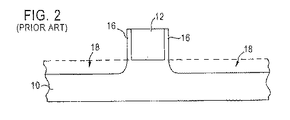
この状況を、図1および図2に概略的に記載する。
図1において、基板10は、その表面上にゲート電極12を有する。絶縁層14は、基板10とゲート電極12を被覆する。
オフセットスペーサ16を形成するため、基板から絶縁材14を取り除く異方性エッチングが実行される。
しかしながら、異方性エッチングプロセスをシリコン上で停止させるのは難しいので、凹部(recess)18はまた、オーバー・エッチングによって引き起こされる基板10の掘り下げによって形成される。
凹部18の形成は、特にソース/ドレイン拡張部の領域において問題となる。
これは、シリコンの掘り下げは、接合深さを増加させることと同じであるためであり、接合深さの増加は、浅い深さの接合が今日の技術において要求されるため、不適当である。
さらに、オフセット・スペーサ生成中に生成される掘り下げは、オーバーラップ・キャパシタンスに悪影響を及ぼす。
窒化物層は、ポリシリコン再酸化層上にたい積される。
窒化物層は異方性エッチングされ、このエッチングは、ゲート電極上に窒化物オフセット・スペーサを形成するように、ポリシリコン再酸化層上で停止する。
窒化物オフセット・スペーサの形成中に、エッチング停止層としてポリシリコン再酸化層を使用することは、本発明の実施形態に従ってシリコン基板の掘り下げを防ぐ。
極薄ポリシリコン再酸化層は基板上に残るようにすることができ、ソース/ドレイン拡張部およびソース/ドレイン領域を形成するように、残っているポリシリコン再酸化層を通じて、制御可能に、確実に、インプラントが行われてもよい。
代替的に、ポリシリコン再酸化層は、通常、絶縁層のドライ・エッチングに関連する掘り下げを生成しないウェット・エッチングによって取り除くこともできる。
窒化物層は基板およびゲート電極上に形成される。
窒化物層は、ゲート電極上にオフセット・スペーサを形成するようにエッチングされ、このエッチングは、エッチング停止層上で停止する。
特に、本発明は、ゲート電極のサイドウォール上にオフセット・スペーサを形成するための絶縁層のエッチング中に発生する掘り下げの問題の一部を解決する。
本発明は、半導体デバイスの基板上に、ポリシリコン再酸化層のようなエッチング停止層を提供することによって、これらの問題の一部を解決する。
窒化物層は、ポリシリコン再酸化層上にたい積される。
窒化物層の異方性エッチングは、ポリシリコン再酸化層上でエッチングが停止するように選択され、ポリシリコン再酸化層を貫通してシリコン基板を掘り下げないようになっている。
ポリシリコン再酸化層は極薄であるので、インプラント・プロセスが、ソース/ドレイン拡張部およびソース/ドレイン領域を形成するように、ポリシリコン再酸化層を通じて、制御可能に、正確に行うことができる。
代替的に、ポリシリコン再酸化層は、シリコン基板を掘り下げる恐れのないウェットエッチング・プロセスによって安全に除去されてもよい。
掘り下げの防止は、ハローと拡張部を分離し、トランジスタのよりよいAC性能を提供すべく、オーバーラップ・キャパシタンスを縮小する。
さらに本発明は、シリコンの掘り下げを防止することによって、浅い深さ形成の効果を維持する。
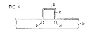
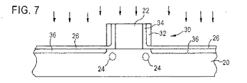
このデバイスは、例えばシリコンからなる基板20を含む。この基板20の上表面上には、例えばポリシリコンからなるゲート電極が提供される。
ポリシリコン・ゲート電極22は従来の方法で形成されてもよいし、その後ポリシリコンまたは他のゲート電極材料がたい積され、ゲート電極22を形成すべくエッチングされる、ゲート酸化膜の形成を含んでいてもよい。
ハロー・インプラント24は、本発明の方法の全体にわたって記載されるが、ハロー・インプラント24は任意のものであり、本発明の実施形態はこのようなハロー・インプラントを有することなく、半導体デバイスを形成することが理解される。
これらの実施形態は、図3ないし図8において記載されていないが、当業者は、本発明の方法がハロー・インプラント24と共に実行されても、ハロー/インプラント24を有することなく実行されてもよいことを認識するだろう。
しかしながら、説明と例示のため、ハロー・インプラント24は、図3ないし図8において示される。
ポリシリコン再酸化ステップは、基板20およびゲート電極22の表面上にポリシリコン再酸化層26を形成する。
ポリシリコン再酸化層26は、従来のポリシリコン再酸化形成プロセスによって形成される。このプロセスは、約750℃から900℃の間の温度で熱処理により成長した酸化層を提供する。
ポリシリコン再酸化層26は、15Åから約50Åの厚みに形成され、好ましくは25Åの厚みに形成される。
ポリシリコン再酸化層26は、後述するその後のエッチングステップにおいて、エッチング停止層として優れた選択性を提供する、非常に高密度で高品質な絶縁層である。
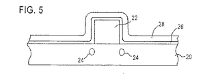
窒化シリコン製とすることができる窒化物層28は、例えば、典型的な技術として、プラズマ強化化学気相たい積法(PECVD)(plasma enhanced chemical vapor deposition)または減圧化学気相たい積法(LPCVD)(low pressure chemical vapor deposition)による従来の方式でたい積することができる。
窒化物は、100Åから500Åの厚みでたい積されてもよい。本発明の実施例の一つにおいては、約250Åの厚みにたい積された窒化物を使用する。
異方性エッチングは、例えばCHF3を使用する、反応性イオン・エッチングであってもよい。
このエッチングは、ゲート電極22および基板20の頂部のような水平表面から、窒化物層28を除去する。
ポリシリコン再酸化層26は、エッチング停止層としての役割を果たすので、エッチングは、ポリシリコン再酸化層26上で停止する。このことは、窒化物層28のエッチングの間、シリコン基板20の掘り下げを防ぐことになる。
先行技術の方法では、前述したように、エッチングは、基板中へと進んで掘り下げおよび凹部を形成することになり、好ましくない結果となる。
ポリシリコン再酸化層26は、エッチャントについての窒化物/酸化物の選択性が、典型的に酸化物/シリコンの選択性または窒化物/シリコンの選択性よりも高いという優れた選択性を提供する。
従って、窒化物層28のエッチングは、ポリシリコン再酸化層26上で正確に停止することができる。
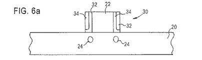
図6Aに示すように、異方性エッチング中にエッチング停止層としての役割を果たしたポリシリコン層26の部分は、ある実施形態において、基板20の上表面を露出すべく、ウェットエッチング・プロセスによって除去されてもよい。
シリコン基板20に破壊的な化学作用を及ぼすことなくポリシリコン再酸化層26を除去する、典型的なウェットエッチング・プロセスは、100:1のHF溶液である。
基板20上のポリシリコン再酸化層26を除去することによって、ソース/ドレイン拡張部およびソース/ドレイン領域のインプラントが妨げられないようになる。
しかしながら、本発明の他の実施形態においては、基板20上のポリシリコン再酸化層26が、基板20上に残るようにしてもよい。
これは、基板上のポリシリコン再酸化層26の厚みが相対的に極薄であるため、ポリシリコン再酸化層26を通じての基板20中へのインプラントが、正確に、制御可能に行うことができるためである。
以下の詳細な説明および図面は、ポリシリコン再酸化層26が基板20に残っているものと仮定するものである。
しかしながら、本発明の他の実施形態は、ポリシリコン再酸化層26を取り除くべく提供されることが明白に理解されるべきである。
このインプラント中、オフセット・スペーサ30は、通常理解されているようにマスクの役割を果たす。
その後、基板20中にソース/ドレイン領域40を形成すべく、ソース/ドレインのインプラントが、実行される。
活性化アニーリング・ステップは従来の方法に従ってインプラントの後に実行される。
これは、絶縁層(この絶縁層から、異方性エッチング・ステップで、オフセット・スペーサがエッチングされる)の下にあるエッチング停止層の使用によって遂行される。
しかしながら、薄いポリシリコンについては、ボロン突き抜けの問題がより悪化する。
さらに、上述したようにポリシリコンは極薄であるので、全てのポリシリコンがシリサイド化される可能性がある。
このことは、ポリシリコン/ゲート酸化膜の界面を粗くし、ゲート酸化膜の信頼性についての問題を引き起こす。
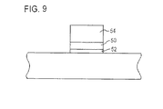
本発明はボロン突き抜けを防ぐため、図9に記載されるように、ゲート酸化膜52上であって、ポリシリコン54のたい積の前に、金属窒化物バリア層50を形成する。
さらに、後のシリサイド化は、この伝導性の金属窒化物バリア層50上で停止する。このプロセスの他の利点には、ポリシリコン消耗がほとんどまたは全くないことが含まれる。
Claims (10)
- 基板(20)上にゲート電極(22)を形成するステップと、
前記基板(20)および前記ゲート電極(22)上にポリシリコン再酸化層(26)を形成するステップと、
前記ポリシリコン再酸化層(26)上に窒化物層(28)をたい積するステップと、
前記窒化物層(28)を異方性エッチングし、前記ゲート電極(22)上に窒化物オフセット・スペーサ(30)を形成するように、前記ポリシリコン再酸化層(26)上で前記異方性エッチングを停止するステップと、
を含む、半導体デバイスを形成する方法。 - 前記窒化物層(28)がエッチングされた後、前記基板(20)中にソース/ドレイン拡張部(36)を形成するステップと、
前記オフセット・スペーサ(30)上にサイドウォール・スペーサ(38)を形成するステップと、
前記基板(20)中にソース/ドレイン(40)を形成するステップとをさらに含む、請求項1記載の方法。 - 前記窒化物層(28)をたい積する前に、前記基板(20)中にハロー・インプラント(24)を形成するステップをさらに含む、請求項2記載の方法。
- 前記ポリシリコン再酸化層を形成するステップは、約700℃から約900℃の間の温度で、酸化物を前記基板および前記ゲート電極上に熱処理によって成長させることを含む、請求項3記載の方法。
- 前記窒化物層(28)をエッチングした後であって、前記基板(20)中に前記ソース/ドレイン拡張部(36)を形成する前に、前記露出したポリシリコン再酸化層を除去するステップをさらに含む、請求項4記載の方法。
- 基板(20)上にゲート電極(22)を形成するステップと、
前記基板(20)上にエッチング停止層(26)を形成するステップと、
前記エッチング停止層(26)上に窒化物層(28)を形成するステップと、
前記ゲート電極(22)上にオフセット・スペーサ(30)を形成するように前記窒化物層(28)をエッチングし、前記エッチングを前記エッチング停止層(26)上で停止するステップと、
前記基板(20)中にハロー・インプラント(24)を形成するステップと、
を含む、ハロー・インプラントを備えた半導体デバイスを形成する方法。 - 前記エッチング停止層(26)は、ポリシリコン再酸化層(26)である、
請求項6記載の方法。 - 前記窒化物層(28)がエッチングされた後、前記ポリシリコン再酸化層(26)を貫通してインプラントすることによって、ソース/ドレイン拡張部(36)およびソース/ドレイン・インプラント(40)を形成するステップをさらに含む、請求項7記載の方法。
- 前記基板(20)を露出するように、前記窒化物層(28)をエッチングすることによって露出した前記ポリシリコン再酸化層(26)の一部を除去するステップをさらに含む、請求項8記載の方法。
- 前記窒化物層(28)をエッチングするステップは、前記窒化物層(28)を、窒化物対酸化物の高い選択性を有するプラズマ・エッチャント・ガスで、反応性イオンエッチングするステップを含む、請求項9記載の方法。
Applications Claiming Priority (2)
| Application Number | Priority Date | Filing Date | Title |
|---|---|---|---|
| US10/023,328 US6780776B1 (en) | 2001-12-20 | 2001-12-20 | Nitride offset spacer to minimize silicon recess by using poly reoxidation layer as etch stop layer |
| PCT/US2002/041105 WO2003054948A1 (en) | 2001-12-20 | 2002-12-19 | Nitride offset spacer to minimize silicon recess by using poly reoxidation layer as etch stop layer |
Publications (2)
| Publication Number | Publication Date |
|---|---|
| JP2005514765A true JP2005514765A (ja) | 2005-05-19 |
| JP2005514765A5 JP2005514765A5 (ja) | 2006-02-09 |
Family
ID=21814449
Family Applications (1)
| Application Number | Title | Priority Date | Filing Date |
|---|---|---|---|
| JP2003555572A Pending JP2005514765A (ja) | 2001-12-20 | 2002-12-19 | エッチング停止層としてポリシリコン再酸化層を使用することによって、シリコン層の凹部を減少する窒化オフセットスペーサ |
Country Status (7)
| Country | Link |
|---|---|
| US (1) | US6780776B1 (ja) |
| EP (1) | EP1456874A1 (ja) |
| JP (1) | JP2005514765A (ja) |
| KR (1) | KR100945915B1 (ja) |
| CN (1) | CN100367470C (ja) |
| AU (1) | AU2002358271A1 (ja) |
| WO (1) | WO2003054948A1 (ja) |
Cited By (1)
| Publication number | Priority date | Publication date | Assignee | Title |
|---|---|---|---|---|
| US8552507B2 (en) | 2009-12-24 | 2013-10-08 | Renesas Electronics Corporation | Semiconductor device and method of manufacturing the same |
Families Citing this family (7)
| Publication number | Priority date | Publication date | Assignee | Title |
|---|---|---|---|---|
| KR100721200B1 (ko) * | 2005-12-22 | 2007-05-23 | 주식회사 하이닉스반도체 | 반도체소자의 듀얼 게이트 형성방법 |
| JP2009527103A (ja) * | 2006-02-14 | 2009-07-23 | エス テ マイクロエレクトロニクス クロル 2 エス アー エス | 閾値が調整可能なmosトランジスタ |
| US7544561B2 (en) * | 2006-11-06 | 2009-06-09 | Taiwan Semiconductor Manufacturing Company, Ltd. | Electron mobility enhancement for MOS devices with nitrided polysilicon re-oxidation |
| KR100874957B1 (ko) * | 2007-02-26 | 2008-12-19 | 삼성전자주식회사 | 오프셋 스페이서를 갖는 반도체 소자의 제조방법 및 관련된소자 |
| JP2008098640A (ja) * | 2007-10-09 | 2008-04-24 | Toshiba Corp | 半導体装置の製造方法 |
| US8854403B2 (en) * | 2009-02-06 | 2014-10-07 | Xerox Corporation | Image forming apparatus with a TFT backplane for xerography without a light source |
| CN108206160B (zh) * | 2016-12-20 | 2020-11-03 | 中芯国际集成电路制造(上海)有限公司 | 一种半导体器件及其制造方法和电子装置 |
Citations (3)
| Publication number | Priority date | Publication date | Assignee | Title |
|---|---|---|---|---|
| JPH053206A (ja) * | 1990-08-29 | 1993-01-08 | Toshiba Corp | オフセツトゲート構造トランジスタおよびその製造方法 |
| JPH05102185A (ja) * | 1991-04-01 | 1993-04-23 | Sgs Thomson Microelectron Inc | 改良型電界効果トランジスタ構成体及び製造方法 |
| JPH07142726A (ja) * | 1993-11-19 | 1995-06-02 | Oki Electric Ind Co Ltd | 電界効果型トランジスタの製造方法 |
Family Cites Families (10)
| Publication number | Priority date | Publication date | Assignee | Title |
|---|---|---|---|---|
| GB2219434A (en) | 1988-06-06 | 1989-12-06 | Philips Nv | A method of forming a contact in a semiconductor device |
| US5783475A (en) * | 1995-11-13 | 1998-07-21 | Motorola, Inc. | Method of forming a spacer |
| US5670404A (en) | 1996-06-21 | 1997-09-23 | Industrial Technology Research Institute | Method for making self-aligned bit line contacts on a DRAM circuit having a planarized insulating layer |
| US5899719A (en) * | 1997-02-14 | 1999-05-04 | United Semiconductor Corporation | Sub-micron MOSFET |
| US6063698A (en) * | 1997-06-30 | 2000-05-16 | Motorola, Inc. | Method for manufacturing a high dielectric constant gate oxide for use in semiconductor integrated circuits |
| US5912188A (en) | 1997-08-04 | 1999-06-15 | Advanced Micro Devices, Inc. | Method of forming a contact hole in an interlevel dielectric layer using dual etch stops |
| US6165831A (en) | 1998-11-20 | 2000-12-26 | United Microelectronics Corp. | Method of fabricating a buried contact in a static random access memory |
| US6187645B1 (en) | 1999-01-19 | 2001-02-13 | United Microelectronics Corp. | Method for manufacturing semiconductor device capable of preventing gate-to-drain capacitance and eliminating birds beak formation |
| US6294432B1 (en) | 1999-12-20 | 2001-09-25 | United Microelectronics Corp. | Super halo implant combined with offset spacer process |
| TW463251B (en) * | 2000-12-08 | 2001-11-11 | Macronix Int Co Ltd | Manufacturing method of gate structure |
-
2001
- 2001-12-20 US US10/023,328 patent/US6780776B1/en not_active Expired - Lifetime
-
2002
- 2002-12-19 EP EP02792509A patent/EP1456874A1/en not_active Withdrawn
- 2002-12-19 CN CNB028257359A patent/CN100367470C/zh not_active Expired - Lifetime
- 2002-12-19 KR KR1020047009735A patent/KR100945915B1/ko active IP Right Grant
- 2002-12-19 WO PCT/US2002/041105 patent/WO2003054948A1/en active Application Filing
- 2002-12-19 JP JP2003555572A patent/JP2005514765A/ja active Pending
- 2002-12-19 AU AU2002358271A patent/AU2002358271A1/en not_active Abandoned
Patent Citations (3)
| Publication number | Priority date | Publication date | Assignee | Title |
|---|---|---|---|---|
| JPH053206A (ja) * | 1990-08-29 | 1993-01-08 | Toshiba Corp | オフセツトゲート構造トランジスタおよびその製造方法 |
| JPH05102185A (ja) * | 1991-04-01 | 1993-04-23 | Sgs Thomson Microelectron Inc | 改良型電界効果トランジスタ構成体及び製造方法 |
| JPH07142726A (ja) * | 1993-11-19 | 1995-06-02 | Oki Electric Ind Co Ltd | 電界効果型トランジスタの製造方法 |
Cited By (1)
| Publication number | Priority date | Publication date | Assignee | Title |
|---|---|---|---|---|
| US8552507B2 (en) | 2009-12-24 | 2013-10-08 | Renesas Electronics Corporation | Semiconductor device and method of manufacturing the same |
Also Published As
| Publication number | Publication date |
|---|---|
| AU2002358271A1 (en) | 2003-07-09 |
| CN1606798A (zh) | 2005-04-13 |
| KR20040068964A (ko) | 2004-08-02 |
| KR100945915B1 (ko) | 2010-03-05 |
| EP1456874A1 (en) | 2004-09-15 |
| CN100367470C (zh) | 2008-02-06 |
| WO2003054948A1 (en) | 2003-07-03 |
| US6780776B1 (en) | 2004-08-24 |
Similar Documents
| Publication | Publication Date | Title |
|---|---|---|
| US6917085B2 (en) | Semiconductor transistor using L-shaped spacer | |
| US6245639B1 (en) | Method to reduce a reverse narrow channel effect for MOSFET devices | |
| KR100498476B1 (ko) | 리세스 채널 mosfet 및 그 제조방법 | |
| JP2007027738A (ja) | 半導体装置及びその製作方法 | |
| US7611949B2 (en) | Method of fabricating metal-oxide-semiconductor transistor | |
| JP2003133549A (ja) | Mosfet及びその製造方法 | |
| TWI396229B (zh) | 用可棄式間隔物之提高的源極與汲極製程 | |
| KR100414735B1 (ko) | 반도체소자 및 그 형성 방법 | |
| KR20080024273A (ko) | 반도체 소자 및 그의 제조방법 | |
| JP2005514765A (ja) | エッチング停止層としてポリシリコン再酸化層を使用することによって、シリコン層の凹部を減少する窒化オフセットスペーサ | |
| JP2002359369A (ja) | 半導体装置の製造方法 | |
| US6455388B1 (en) | Method of manufacturing metal-oxide semiconductor transistor | |
| US20080070356A1 (en) | Trench replacement gate process for transistors having elevated source and drain regions | |
| US11387338B1 (en) | Methods for forming planar metal-oxide-semiconductor field-effect transistors | |
| KR100488099B1 (ko) | 쇼오트 채널 모오스 트랜지스터 및 그 제조 방법 | |
| KR100313546B1 (ko) | 트랜지스터 형성방법 | |
| KR20020045260A (ko) | 반도체 소자의 게이트 전극 형성 방법 | |
| JP2594772B2 (ja) | Mos素子およびその製造方法 | |
| JP2000077429A (ja) | 半導体装置の製造方法 | |
| KR100800950B1 (ko) | 반도체 소자의 게이트 전극 제조 방법 | |
| JP2007188956A (ja) | 半導体装置の製造方法 | |
| KR20050053249A (ko) | 반도체 장치의 트랜지스터 형성 방법 | |
| KR100467812B1 (ko) | 반도체 소자 및 그 제조 방법 | |
| JP2008193013A (ja) | 半導体装置及びその製造方法 | |
| JP2006237453A (ja) | 半導体装置及びその製造方法 |
Legal Events
| Date | Code | Title | Description |
|---|---|---|---|
| A521 | Written amendment |
Free format text: JAPANESE INTERMEDIATE CODE: A523 Effective date: 20051215 |
|
| A621 | Written request for application examination |
Free format text: JAPANESE INTERMEDIATE CODE: A621 Effective date: 20051215 |
|
| A977 | Report on retrieval |
Free format text: JAPANESE INTERMEDIATE CODE: A971007 Effective date: 20071106 |
|
| A131 | Notification of reasons for refusal |
Free format text: JAPANESE INTERMEDIATE CODE: A131 Effective date: 20091104 |
|
| A601 | Written request for extension of time |
Free format text: JAPANESE INTERMEDIATE CODE: A601 Effective date: 20100203 |
|
| A602 | Written permission of extension of time |
Free format text: JAPANESE INTERMEDIATE CODE: A602 Effective date: 20100210 |
|
| A601 | Written request for extension of time |
Free format text: JAPANESE INTERMEDIATE CODE: A601 Effective date: 20100304 |
|
| A602 | Written permission of extension of time |
Free format text: JAPANESE INTERMEDIATE CODE: A602 Effective date: 20100311 |
|
| A521 | Written amendment |
Free format text: JAPANESE INTERMEDIATE CODE: A523 Effective date: 20100405 |
|
| RD03 | Notification of appointment of power of attorney |
Free format text: JAPANESE INTERMEDIATE CODE: A7423 Effective date: 20100421 |
|
| A02 | Decision of refusal |
Free format text: JAPANESE INTERMEDIATE CODE: A02 Effective date: 20100526 |
|
| RD05 | Notification of revocation of power of attorney |
Free format text: JAPANESE INTERMEDIATE CODE: A7425 Effective date: 20100902 |
|
| A521 | Written amendment |
Free format text: JAPANESE INTERMEDIATE CODE: A523 Effective date: 20100924 |
|
| A911 | Transfer to examiner for re-examination before appeal (zenchi) |
Free format text: JAPANESE INTERMEDIATE CODE: A911 Effective date: 20101109 |
|
| A912 | Re-examination (zenchi) completed and case transferred to appeal board |
Free format text: JAPANESE INTERMEDIATE CODE: A912 Effective date: 20101210 |