JP2005333063A - クランプ部材、成膜装置、成膜方法、半導体装置の製造方法 - Google Patents
クランプ部材、成膜装置、成膜方法、半導体装置の製造方法 Download PDFInfo
- Publication number
- JP2005333063A JP2005333063A JP2004151953A JP2004151953A JP2005333063A JP 2005333063 A JP2005333063 A JP 2005333063A JP 2004151953 A JP2004151953 A JP 2004151953A JP 2004151953 A JP2004151953 A JP 2004151953A JP 2005333063 A JP2005333063 A JP 2005333063A
- Authority
- JP
- Japan
- Prior art keywords
- wafer
- substrate
- rotating member
- clamp ring
- clamp
- Prior art date
- Legal status (The legal status is an assumption and is not a legal conclusion. Google has not performed a legal analysis and makes no representation as to the accuracy of the status listed.)
- Withdrawn
Links
Images


Classifications
-
- H—ELECTRICITY
- H10—SEMICONDUCTOR DEVICES; ELECTRIC SOLID-STATE DEVICES NOT OTHERWISE PROVIDED FOR
- H10P—GENERIC PROCESSES OR APPARATUS FOR THE MANUFACTURE OR TREATMENT OF DEVICES COVERED BY CLASS H10
- H10P72/00—Handling or holding of wafers, substrates or devices during manufacture or treatment thereof
- H10P72/70—Handling or holding of wafers, substrates or devices during manufacture or treatment thereof for supporting or gripping
- H10P72/76—Handling or holding of wafers, substrates or devices during manufacture or treatment thereof for supporting or gripping using mechanical means, e.g. clamps or pinches
- H10P72/7604—Handling or holding of wafers, substrates or devices during manufacture or treatment thereof for supporting or gripping using mechanical means, e.g. clamps or pinches the wafers being placed on a susceptor, stage or support
- H10P72/7608—Handling or holding of wafers, substrates or devices during manufacture or treatment thereof for supporting or gripping using mechanical means, e.g. clamps or pinches the wafers being placed on a susceptor, stage or support characterised by a plurality of separate clamping members, e.g. clamping fingers
-
- C—CHEMISTRY; METALLURGY
- C23—COATING METALLIC MATERIAL; COATING MATERIAL WITH METALLIC MATERIAL; CHEMICAL SURFACE TREATMENT; DIFFUSION TREATMENT OF METALLIC MATERIAL; COATING BY VACUUM EVAPORATION, BY SPUTTERING, BY ION IMPLANTATION OR BY CHEMICAL VAPOUR DEPOSITION, IN GENERAL; INHIBITING CORROSION OF METALLIC MATERIAL OR INCRUSTATION IN GENERAL
- C23C—COATING METALLIC MATERIAL; COATING MATERIAL WITH METALLIC MATERIAL; SURFACE TREATMENT OF METALLIC MATERIAL BY DIFFUSION INTO THE SURFACE, BY CHEMICAL CONVERSION OR SUBSTITUTION; COATING BY VACUUM EVAPORATION, BY SPUTTERING, BY ION IMPLANTATION OR BY CHEMICAL VAPOUR DEPOSITION, IN GENERAL
- C23C14/00—Coating by vacuum evaporation, by sputtering or by ion implantation of the coating forming material
- C23C14/22—Coating by vacuum evaporation, by sputtering or by ion implantation of the coating forming material characterised by the process of coating
- C23C14/50—Substrate holders
Landscapes
- Chemical & Material Sciences (AREA)
- Chemical Kinetics & Catalysis (AREA)
- Engineering & Computer Science (AREA)
- Materials Engineering (AREA)
- Mechanical Engineering (AREA)
- Metallurgy (AREA)
- Organic Chemistry (AREA)
- Container, Conveyance, Adherence, Positioning, Of Wafer (AREA)
- Physical Vapour Deposition (AREA)
Priority Applications (2)
| Application Number | Priority Date | Filing Date | Title |
|---|---|---|---|
| JP2004151953A JP2005333063A (ja) | 2004-05-21 | 2004-05-21 | クランプ部材、成膜装置、成膜方法、半導体装置の製造方法 |
| US11/133,452 US20050257746A1 (en) | 2004-05-21 | 2005-05-20 | Clamp member, film deposition apparatus, film deposition method, and semiconductor device manufacturing method |
Applications Claiming Priority (1)
| Application Number | Priority Date | Filing Date | Title |
|---|---|---|---|
| JP2004151953A JP2005333063A (ja) | 2004-05-21 | 2004-05-21 | クランプ部材、成膜装置、成膜方法、半導体装置の製造方法 |
Publications (2)
| Publication Number | Publication Date |
|---|---|
| JP2005333063A true JP2005333063A (ja) | 2005-12-02 |
| JP2005333063A5 JP2005333063A5 (https=) | 2007-06-21 |
Family
ID=35373981
Family Applications (1)
| Application Number | Title | Priority Date | Filing Date |
|---|---|---|---|
| JP2004151953A Withdrawn JP2005333063A (ja) | 2004-05-21 | 2004-05-21 | クランプ部材、成膜装置、成膜方法、半導体装置の製造方法 |
Country Status (2)
| Country | Link |
|---|---|
| US (1) | US20050257746A1 (https=) |
| JP (1) | JP2005333063A (https=) |
Cited By (2)
| Publication number | Priority date | Publication date | Assignee | Title |
|---|---|---|---|---|
| JP2010225740A (ja) * | 2009-03-23 | 2010-10-07 | Tokyo Electron Ltd | 基板処理方法および基板処理装置 |
| KR20190090690A (ko) | 2018-01-25 | 2019-08-02 | 에이블릭 가부시키가이샤 | 반도체 제조 장치 및 반도체 장치의 성막 방법 |
Families Citing this family (6)
| Publication number | Priority date | Publication date | Assignee | Title |
|---|---|---|---|---|
| TWI470110B (zh) * | 2012-09-07 | 2015-01-21 | Manz Taiwan Ltd | 用於化學沉積設備的夾固裝置 |
| JP6870531B2 (ja) * | 2017-08-21 | 2021-05-12 | 三菱電機株式会社 | パワーモジュールおよび電力変換装置 |
| CN107937881B (zh) * | 2017-11-20 | 2019-07-05 | 深圳市华星光电半导体显示技术有限公司 | 基板夹紧装置 |
| US11996315B2 (en) * | 2020-11-18 | 2024-05-28 | Applied Materials, Inc. | Thin substrate handling via edge clamping |
| USD1038049S1 (en) | 2020-11-18 | 2024-08-06 | Applied Materials, Inc. | Cover ring for use in semiconductor processing chamber |
| CN113903649B (zh) * | 2021-09-23 | 2024-04-12 | 北京北方华创微电子装备有限公司 | 半导体工艺设备 |
Family Cites Families (7)
| Publication number | Priority date | Publication date | Assignee | Title |
|---|---|---|---|---|
| US5513594A (en) * | 1993-10-20 | 1996-05-07 | Mcclanahan; Adolphus E. | Clamp with wafer release for semiconductor wafer processing equipment |
| US5437757A (en) * | 1994-01-21 | 1995-08-01 | Applied Materials, Inc. | Clamp ring for domed pedestal in wafer processing chamber |
| DE4420050C1 (de) * | 1994-06-08 | 1995-08-24 | Weidmueller Interface | Abisoliervorrichtung |
| JP3471543B2 (ja) * | 1996-11-07 | 2003-12-02 | 大日本スクリーン製造株式会社 | 回転式基板乾燥装置 |
| US5922133A (en) * | 1997-09-12 | 1999-07-13 | Applied Materials, Inc. | Multiple edge deposition exclusion rings |
| US6699375B1 (en) * | 2000-06-29 | 2004-03-02 | Applied Materials, Inc. | Method of extending process kit consumable recycling life |
| JP4488646B2 (ja) * | 2001-04-23 | 2010-06-23 | 株式会社トプコン | ウェーハ保持装置 |
-
2004
- 2004-05-21 JP JP2004151953A patent/JP2005333063A/ja not_active Withdrawn
-
2005
- 2005-05-20 US US11/133,452 patent/US20050257746A1/en not_active Abandoned
Cited By (2)
| Publication number | Priority date | Publication date | Assignee | Title |
|---|---|---|---|---|
| JP2010225740A (ja) * | 2009-03-23 | 2010-10-07 | Tokyo Electron Ltd | 基板処理方法および基板処理装置 |
| KR20190090690A (ko) | 2018-01-25 | 2019-08-02 | 에이블릭 가부시키가이샤 | 반도체 제조 장치 및 반도체 장치의 성막 방법 |
Also Published As
| Publication number | Publication date |
|---|---|
| US20050257746A1 (en) | 2005-11-24 |
Similar Documents
| Publication | Publication Date | Title |
|---|---|---|
| JP4358108B2 (ja) | コーティング装置における搭載、支持及び取り出しのための一組の器具 | |
| US9099513B2 (en) | Substrate processing apparatus, and substrate processing method | |
| JP3955532B2 (ja) | 加工物の湿式処理 | |
| TWI570835B (zh) | 用於基板處理室的兩片擋板盤組件 | |
| TW202003892A (zh) | 具有整合遮件庫的預清洗腔室 | |
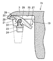
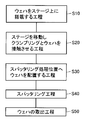
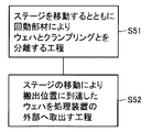
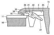
| JP2005333063A (ja) | クランプ部材、成膜装置、成膜方法、半導体装置の製造方法 | |
| JP6513048B2 (ja) | 液処理装置 | |
| TWI829685B (zh) | 具有自定心特徵的兩件式快門盤組件 | |
| TW201407713A (zh) | 基板保持環握持機構 | |
| JP5194315B2 (ja) | スパッタリング装置 | |
| JP4101524B2 (ja) | 成膜装置 | |
| JP6098491B2 (ja) | 半導体製造装置 | |
| JP2003197716A (ja) | 基板支持装置及び半導体製造装置 | |
| JP2001181845A (ja) | 成膜装置 | |
| JP2003282680A (ja) | 基板リフター、クランプリング及び基板処理装置 | |
| EP3361496A1 (en) | Heat treatment vessel for single-crystal silicon carbide substrate and etching method | |
| JP2006186023A (ja) | ウェハ把持具およびウェハ移載装置 | |
| JP7038013B2 (ja) | 基板支持機構 | |
| JP4441158B2 (ja) | 基板ホルダー | |
| JP3904647B2 (ja) | 基板支持装置及びこの基板支持装置に基板を着脱する基板着脱装置並びに基板着脱方法 | |
| JP2007190593A (ja) | 基板保持装置及び基板加工装置 | |
| CN110233119B (zh) | 基板处理装置 | |
| JP4323990B2 (ja) | クランプリング | |
| JPS6319321Y2 (https=) | ||
| US20060144337A1 (en) | Heater for heating a wafer and method for preventing contamination of the heater |
Legal Events
| Date | Code | Title | Description |
|---|---|---|---|
| A521 | Request for written amendment filed |
Free format text: JAPANESE INTERMEDIATE CODE: A523 Effective date: 20070508 |
|
| A621 | Written request for application examination |
Free format text: JAPANESE INTERMEDIATE CODE: A621 Effective date: 20070508 |
|
| A761 | Written withdrawal of application |
Free format text: JAPANESE INTERMEDIATE CODE: A761 Effective date: 20090226 |