JP2005333063A - Clamp member, film forming device, film forming method, and method for manufacturing semiconductor device - Google Patents
Clamp member, film forming device, film forming method, and method for manufacturing semiconductor device Download PDFInfo
- Publication number
- JP2005333063A JP2005333063A JP2004151953A JP2004151953A JP2005333063A JP 2005333063 A JP2005333063 A JP 2005333063A JP 2004151953 A JP2004151953 A JP 2004151953A JP 2004151953 A JP2004151953 A JP 2004151953A JP 2005333063 A JP2005333063 A JP 2005333063A
- Authority
- JP
- Japan
- Prior art keywords
- wafer
- substrate
- rotating member
- clamp ring
- clamp
- Prior art date
- Legal status (The legal status is an assumption and is not a legal conclusion. Google has not performed a legal analysis and makes no representation as to the accuracy of the status listed.)
- Withdrawn
Links
Images


Classifications
-
- H—ELECTRICITY
- H01—ELECTRIC ELEMENTS
- H01L—SEMICONDUCTOR DEVICES NOT COVERED BY CLASS H10
- H01L21/00—Processes or apparatus adapted for the manufacture or treatment of semiconductor or solid state devices or of parts thereof
- H01L21/67—Apparatus specially adapted for handling semiconductor or electric solid state devices during manufacture or treatment thereof; Apparatus specially adapted for handling wafers during manufacture or treatment of semiconductor or electric solid state devices or components ; Apparatus not specifically provided for elsewhere
- H01L21/683—Apparatus specially adapted for handling semiconductor or electric solid state devices during manufacture or treatment thereof; Apparatus specially adapted for handling wafers during manufacture or treatment of semiconductor or electric solid state devices or components ; Apparatus not specifically provided for elsewhere for supporting or gripping
- H01L21/687—Apparatus specially adapted for handling semiconductor or electric solid state devices during manufacture or treatment thereof; Apparatus specially adapted for handling wafers during manufacture or treatment of semiconductor or electric solid state devices or components ; Apparatus not specifically provided for elsewhere for supporting or gripping using mechanical means, e.g. chucks, clamps or pinches
- H01L21/68714—Apparatus specially adapted for handling semiconductor or electric solid state devices during manufacture or treatment thereof; Apparatus specially adapted for handling wafers during manufacture or treatment of semiconductor or electric solid state devices or components ; Apparatus not specifically provided for elsewhere for supporting or gripping using mechanical means, e.g. chucks, clamps or pinches the wafers being placed on a susceptor, stage or support
- H01L21/68728—Apparatus specially adapted for handling semiconductor or electric solid state devices during manufacture or treatment thereof; Apparatus specially adapted for handling wafers during manufacture or treatment of semiconductor or electric solid state devices or components ; Apparatus not specifically provided for elsewhere for supporting or gripping using mechanical means, e.g. chucks, clamps or pinches the wafers being placed on a susceptor, stage or support characterised by a plurality of separate clamping members, e.g. clamping fingers
-
- C—CHEMISTRY; METALLURGY
- C23—COATING METALLIC MATERIAL; COATING MATERIAL WITH METALLIC MATERIAL; CHEMICAL SURFACE TREATMENT; DIFFUSION TREATMENT OF METALLIC MATERIAL; COATING BY VACUUM EVAPORATION, BY SPUTTERING, BY ION IMPLANTATION OR BY CHEMICAL VAPOUR DEPOSITION, IN GENERAL; INHIBITING CORROSION OF METALLIC MATERIAL OR INCRUSTATION IN GENERAL
- C23C—COATING METALLIC MATERIAL; COATING MATERIAL WITH METALLIC MATERIAL; SURFACE TREATMENT OF METALLIC MATERIAL BY DIFFUSION INTO THE SURFACE, BY CHEMICAL CONVERSION OR SUBSTITUTION; COATING BY VACUUM EVAPORATION, BY SPUTTERING, BY ION IMPLANTATION OR BY CHEMICAL VAPOUR DEPOSITION, IN GENERAL
- C23C14/00—Coating by vacuum evaporation, by sputtering or by ion implantation of the coating forming material
- C23C14/22—Coating by vacuum evaporation, by sputtering or by ion implantation of the coating forming material characterised by the process of coating
- C23C14/50—Substrate holders
Landscapes
- Engineering & Computer Science (AREA)
- Chemical & Material Sciences (AREA)
- Condensed Matter Physics & Semiconductors (AREA)
- General Physics & Mathematics (AREA)
- Mechanical Engineering (AREA)
- Metallurgy (AREA)
- Organic Chemistry (AREA)
- Physics & Mathematics (AREA)
- Chemical Kinetics & Catalysis (AREA)
- Materials Engineering (AREA)
- Manufacturing & Machinery (AREA)
- Computer Hardware Design (AREA)
- Microelectronics & Electronic Packaging (AREA)
- Power Engineering (AREA)
- Physical Vapour Deposition (AREA)
- Container, Conveyance, Adherence, Positioning, Of Wafer (AREA)
Abstract
Description
この発明は、クランプ部材、成膜装置、成膜方法、半導体装置の製造方法に関し、より特定的には、成膜工程において基板を保持するクランプ部材、成膜装置、成膜方法、半導体装置の製造方法に関する。 The present invention relates to a clamp member, a film formation apparatus, a film formation method, and a semiconductor device manufacturing method, and more specifically, a clamp member, a film formation apparatus, a film formation method, and a semiconductor device for holding a substrate in a film formation process. It relates to a manufacturing method.
従来、成膜装置において基板(ウェハ)を保持するクランプ部材が知られている(たとえば、特許文献1参照)。 Conventionally, a clamp member that holds a substrate (wafer) in a film forming apparatus is known (see, for example, Patent Document 1).
特許文献1では、クランプ部材として、水平状態から垂直状態にアームを介して回動可能なウェハ載置用円形台と、ウェハ載置台の水平状態での中心軸とその中心軸を同一にする駆動用固定台と、ウェハ載置台の周囲近傍に回動アームが水平状態から垂直状態に移行した時に内側に臥せる少なくとも1対の対向するウェハ把持手段としての爪と、回動アームを水平にした時、爪を開放するガイドとを供えるものが開示されている。
上述したクランプ部材は、基板を垂直状態にして成膜を行なうため、クランプ部材の構造が比較的複雑であった。また、上述したクランプ部材においては、成膜処理の後、爪がガイドの下方に移動することで爪による基板の把持を解消するとしているが、基板から爪にかけて成膜処理により膜が形成されることに起因する爪と基板との固着を解除するため、基板を押圧するなどの能動的な動作を行なうわけではないため、爪と基板との固着が解除されない不具合が発生する可能性が考えられる。 Since the above-described clamp member forms a film with the substrate in a vertical state, the structure of the clamp member is relatively complicated. Further, in the above-described clamp member, after the film formation process, the nail is moved below the guide so as to eliminate the holding of the substrate by the nail, but a film is formed by the film formation process from the substrate to the nail. In order to release the sticking between the nail and the substrate, the active operation such as pressing the substrate is not performed, and there is a possibility that the sticking between the nail and the substrate is not released. .
この発明は、上記のような課題を解決するために成されたものであり、この発明の目的は、簡単な構造でかつ確実に基板との固着を解消することが可能なクランプ部材および当該クランプ部材を用いた成膜装置、成膜方法、半導体装置の製造方法を提供することである。 The present invention has been made to solve the above-described problems, and an object of the present invention is to provide a clamp member and a clamp that can be reliably removed from the substrate with a simple structure. It is to provide a film forming apparatus using a member, a film forming method, and a method for manufacturing a semiconductor device.
この発明に従ったクランプ部材は、基板に対する処理を行なう際に基板を保持するクランプ部材であって、基板を保持するための保持部と、保持部に配置された回転軸と、回動部材とを備える。回動部材は、回転軸を中心として回転可能であり、一方端部と他方端部とを有する。回動部材は、保持部が基板を保持しているときに基板の一部と間隔を隔てて重なる位置に一方端部が位置するように配置される。回動部材は、保持部が基板を保持しているときに、他方端部を保持部に向けて押圧することにより回転軸を中心として回転した結果、一方端部が基板の一部を保持部から離れる方向に押圧することが可能である。 A clamp member according to the present invention is a clamp member that holds a substrate when performing processing on the substrate, and includes a holding portion for holding the substrate, a rotating shaft disposed in the holding portion, and a rotating member. Is provided. The rotating member is rotatable about the rotation axis and has one end and the other end. The rotating member is arranged so that one end portion thereof is located at a position overlapping with a part of the substrate with a gap when the holding portion holds the substrate. The rotating member rotates around the rotation axis by pressing the other end portion toward the holding portion when the holding portion holds the substrate, so that the one end portion holds the part of the substrate. It is possible to press away from the direction.
このように、本発明によれば、回動部材の一方端部により基板の一部を押圧することにより、クランプ部材と基板との分離を確実に行なうことができるため、当該クランプ部材が設置された処理装置においてクランプ部材と基板との分離ができないといった問題の発生確率を低減できる。 As described above, according to the present invention, the clamp member and the substrate can be reliably separated by pressing a part of the substrate with the one end portion of the rotating member. In such a processing apparatus, it is possible to reduce the probability of occurrence of a problem that the clamp member and the substrate cannot be separated.
以下、図面に基づいて本発明の実施の形態を説明する。なお、以下の図面において同一または相当する部分には同一の参照番号を付しその説明は繰返さない。 Hereinafter, embodiments of the present invention will be described with reference to the drawings. In the following drawings, the same or corresponding parts are denoted by the same reference numerals, and description thereof will not be repeated.
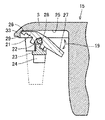
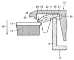
図1は、本発明によるクランプリングを備えるスパッタリング装置を示す断面模式図である。図2および図3は、図1に示したスパッタリング装置におけるクランプリングの部分断面模式図である。図1〜図3を参照して、本発明によるクランプリングおよびスパッタリング装置を説明する。本発明による半導体装置の製造装置としてのスパッタリング装置1は、図1に示すように、ロアーシールド体13とこのロアーシールド体13の上部に形成された開口部を塞ぐように配置された蓋部材14とからなるチャンバを備える。このチャンバ内部には、矢印20に示した方向に昇降可能なステージ16が配置されている。このステージ16は、ベース部17上に搭載されている。このステージ16上には被処理対象物であるシリコンからなるウェハ11が搭載される。
FIG. 1 is a schematic cross-sectional view showing a sputtering apparatus including a clamp ring according to the present invention. 2 and 3 are schematic partial cross-sectional views of the clamp ring in the sputtering apparatus shown in FIG. The clamp ring and sputtering apparatus according to the present invention will be described with reference to FIGS. As shown in FIG. 1, a sputtering apparatus 1 as a semiconductor device manufacturing apparatus according to the present invention includes a
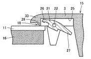
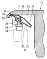
そして、このウェハ11の外縁部を押圧固定するため、クランプリング15が配置されている。また、ステージ16と対向する位置である蓋部材14の内周面上にはスパッタリングを行なうためのターゲット材12が配置されている。ターゲット材12の材質は、ウェハ11表面に形成する膜の材質に合せて適宜選択できる。たとえば、ターゲット材12としてアルミニウムまたはアルミニウム合金を用いることができる。また、チャンバを構成するロアーシールド体13の開口部7と対向する位置に、ウェハ11の搬送に用いるリフター10が配置されている。クランプリング15においてウェハ11と対向する内周側フランジ部3の端部(内周側の端部におけるウェハ11と対向する下面部分)には、ウェハ11を押圧するクランプ部29と、このクランプ部29よりも外側の領域に形成された凹部25の内部に位置する回動部材21とが配置されている。
A
回動部材21は、クランプリング15と同じ材料で構成されることが好ましい。たとえば回動部材21およびクランプリング15はステンレス鋼を用いて形成できる。なお、回動部材21を構成する材料として、他の線膨張係数の値が相対的に小さな任意の材料を用いても良い。回動部材21は、先端部26と、この先端部26と反対側に位置する後端部27と、この先端部26および後端部27の間に形成された溝28とを備える。この溝28は回転軸22と嵌合する。回転軸22は、押え板23によってクランプリング15へと押圧されることにより固定されている。押え板23はネジ24によりクランプリング15へと固定されている。回動部材21は、回転軸22を中心として矢印19に示す方向に回動可能となっている。また、回動部材21に対して特に外部からの応力が加わっていない場合には、図2に示すように後端部27が下がった状態(図2に示す状態)となるように、溝28より外側(後端部27側)に回動部材21の重心は位置している。一方、チャンバを構成するロアーシールド体13上にクランプリング15が搭載されたときには、回動部材21の後端部27をロアーシールド体13の側壁8が押圧する状態となる。このため、図3に示すように、回動部材21の後端部27が押上げられ、回動部材21の先端部26が下向き(矢印9に示す方向)に移動する。この結果、回動部材21の先端部26はクランプ部29の下端より下側に突出する位置にまで移動できる。
The rotating
また、クランプリング15の内周側において、ウェハ11の表面と接触するクランプ部29からウェハ11の中央部方向へと延びる(突出する)ように、凸部33が形成されている。このような凸部33が形成されているため、ウェハ11に対するスパッタリング工程の際に、ターゲット材12から飛散した原子がクランプ部29とウェハ11との接触部などにまで到達することによりクランプ部29や回動部材21の表面にまでスパッタリングに起因する膜が形成される可能性を低減できる。このため、ウェハ11上からクランプ部29表面にまで延材するように(ウェハ11とクランプ部29との接続部上に)スパッタリングによって形成された膜により、ウェハ11とクランプ部29とが固着する可能性を低減できる。
Further, on the inner peripheral side of the
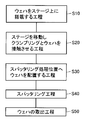
次に、図1〜図3に示したスパッタリング装置1を用いたスパッタリング方法を図4〜図8を参照しながら説明する。図4は、図1〜図3に示したスパッタリング装置を用いたスパッタリング方法を示すフローチャートである。図5は、図4に示したウェハの取出工程の内容を示すフローチャートである。図6は、図4に示したクランプリングとウェハを接触させる工程におけるクランプリングとウェハとの接触状況を示すクランプリングの部分断面模式図である。図7は、図6に示したクランプリングの動作を説明するためのクランプリングの部分断面模式図である。図8は、図4に示したウェハの取出工程を説明するためのクランプリングの部分断面模式図である。 Next, a sputtering method using the sputtering apparatus 1 shown in FIGS. 1 to 3 will be described with reference to FIGS. FIG. 4 is a flowchart showing a sputtering method using the sputtering apparatus shown in FIGS. FIG. 5 is a flowchart showing the contents of the wafer removal process shown in FIG. FIG. 6 is a schematic partial cross-sectional view of the clamp ring showing a contact state between the clamp ring and the wafer in the step of contacting the clamp ring and the wafer shown in FIG. FIG. 7 is a partial cross-sectional schematic view of the clamp ring for explaining the operation of the clamp ring shown in FIG. FIG. 8 is a partial cross-sectional schematic view of the clamp ring for explaining the wafer removal step shown in FIG.
図1に示したスパッタリング装置を用いたスパッタリング方法では、まず、図4に示すようにウェハをステージ上に搭載する工程(S10)を実施する。このとき、図1に示したスパッタリング装置1では、ステージ16はロアーシールド体13の開口部7よりも下側(すなわちロアーシールド体13の外側)に配置されている。そして、リフター10にウェハ搬送ロボットによって処理対象物であるウェハ11(図1参照)が配置される。次に、ステージ16が上昇し、上述のリフター10に保持されていたウェハ11をそのステージ16の上部表面上に搭載する。なお、このときクランプリング15はロアーシールド体13の側壁8上に載った状態(図3に示したような状態)となっている。
In the sputtering method using the sputtering apparatus shown in FIG. 1, first, a step (S10) of mounting a wafer on a stage is performed as shown in FIG. At this time, in the sputtering apparatus 1 shown in FIG. 1, the
次に、ステージ16をさらに上方へ(チャンバ内部方向へ)移動し、クランプリングとウェハを接触させる工程(S20)を実施する。この工程(S20)では、具体的にはステージ16をさらに上昇させることにより、図6に示すようにクランプリング15のクランプ部29とステージ16上に配置されたウェハ11の端部とが接触する。
Next, the
なお、このとき、図3に示したようにクランプリング15は予めロアーシールド体13の側壁8上に載った状態であり、回動部材21の先端部26は図3に示すようにクランプリング15のクランプ部29よりも下に下がった(突出した)状態となっている。そのため、実際には、ステージ16の上昇に伴って上昇してきたウェハ11の端部と最初に接触するのは回動部材21の先端部26である。そして、ステージ16のさらなる上昇に伴って、回動部材21の先端部26はウェハ11の端部に押されることにより先端部26が上昇するように回動部材21が回転軸22を中心として回転する。また、このとき同時にクランプリング15が徐々にウェハ11に押されることにより上方へと持上げられることになる。
At this time, as shown in FIG. 3, the
そして、ステージ16の上昇に伴ってウェハ11がさらに上昇し、ウェハ11の端部がクランプリング15のクランプ部29と接触する。ステージ16がさらに上昇することにより、クランプリング15がロアーシールド体13の側壁8から持上げられると、回動部材21の後端部27とロアーシールド体13の側壁8の上端部とが離れることになる。この結果、図6に示すように、クランプリング15に設置された回動部材21の先端部26とウェハ11の端部とは間隔を隔てて対向した状態(離れた状態)となる。これは、図7に示すように、回動部材21に対して外部から力が加えられていない状態のときには、回動部材21の重心が回転軸22よりも後端部27側に位置するため、先端部26の方が後端部27よりも上方(クランプリング15の上部表面寄り)に位置するように、回動部材21が配置されるためである。
As the
次に、スパッタリング処理位置へウェハを配置する工程(S30)を実施する。具体的には、ステージ16をさらに上昇させ、ウェハ11に対してスパッタリング処理を施すための所定位置(たとえば、図1に示すような位置)にウェハ11を配置する。
Next, a step (S30) of placing the wafer at the sputtering processing position is performed. Specifically, the
次に、スパッタリング工程(S40)を実施する。このスパッタリング工程(S40)においては、たとえばイオンなどをターゲット材12に入射させ、ターゲット材12を構成する材料の粒子(原子)を飛散させ、当該飛散した粒子(原子)をウェハ11の表面に固着成長させることにより、ウェハ11の表面に膜を形成する。たとえば、ターゲット材12を構成する材料としてアルミニウムを用いる場合、当該ターゲット材12から飛散したアルミニウム粒子をウェハ11の表面に固着成長させることで、アルミニウム膜を形成できる。なお、このスパッタリング工程(S40)においては、従来用いられている任意のスパッタリング方法を用いることができる。
Next, a sputtering step (S40) is performed. In this sputtering step (S40), for example, ions or the like are incident on the
このようにして、ウェハ11の表面上に所定の膜厚の膜を成膜するスパッタリング工程(S40)が終了した後、スパッタリング装置1からウェハ11を取出すウェハの取出工程(S50)を実施する。具体的には、成膜処理が終了したウェハ11を搭載するステージ16を、チャンバの外部へと取出す方向(図1において開口部7を介してチャンバの内部からチャンバの外部へと向かう方向)に移動させる。
In this way, after the sputtering step (S40) for forming a film with a predetermined film thickness on the surface of the
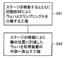
ここで、ウェハの取出工程(S50)の内容をより詳しく説明すると、ウェハの取出工程(S50)では、図5に示すように、ステージ16を移動するとともに回動部材21によりウェハ11とクランプリング15とを分離する工程(S51)が実施される。具体的には、図8に示すように、ステージ16がクランプリング15と共に矢印30に示す方向に降下することにより、クランプリング15に設置された回動部材21の後端部27をロアーシールド体13の側壁8の先端部が押圧することになる。この結果、回動部材21は回転軸22を中心として矢印34に示す方向に回転する(つまり、回転軸22を支点とし、後端部27を力点とし、先端部26を作用としたテコとして、回動部材21が作用する)。そして、回動部材21の先端部26がウェハ11の端部を押圧することにより、ウェハ11とクランプリング15のクランプ部29とを確実に分離できる。
Here, the contents of the wafer take-out process (S50) will be described in more detail. In the wafer take-out process (S50), the
なお、図11に示すように、本発明のような回動部材21(図8参照)を有しないクランプリング115を用いてステージ116上に搭載されたウェハ111を押圧固定している場合には、スパッタリング工程においてウェハ111上に成膜された膜がクランプリング115とウェハ111との接触部118にまで形成される場合がある。この場合、形成された膜によりクランプリング115とウェハ111とが接続された状態となり、ステージ116を下降させることのみではクランプリング115とウェハ111とを分離することが困難になる場合があった。しかし、本発明によれば、図8に示したように回動部材21の先端部26によりウェハ11の端部を押圧できるので、クランプリング15とウェハ11とを確実に分離することができる。ここで、図11は、本発明によるクランプリングの効果を説明するための、比較例としてのクランプリングを示す部分断面模式図である。
As shown in FIG. 11, when the
次に、ウェハの取出工程(S50)として、ステージ16の移動による搬出位置に到達したウェハ11を、処理装置(スパッタリング装置1)の外部へ取出す工程(S52)を実施する。具体的には、クランプリング15から分離されたウェハ11を搭載したステージ16を、チャンバ外部の所定位置(搬出位置)にまで移動させる。この結果、リフター上に成膜処理されたウェハ11が搭載されることになり、搬出用の移動装置(ウェハ搬送ロボットなど)を用いて、成膜処理の終了したウェハ11をスパッタリング装置1の外部へ取出す。
Next, as a wafer take-out step (S50), a step (S52) of taking out the
このようにして、図1〜図3に示したスパッタリング装置1を用いたスパッタリング工程を実施することができる。 In this manner, the sputtering process using the sputtering apparatus 1 shown in FIGS. 1 to 3 can be performed.
次に、図9を参照して、本発明によるスパッタリング装置に設置されるクランプリングの第1の変形例を説明する。図9は、本発明によるスパッタリング装置に配置されるクランプリングの第1の変形例を示す部分断面模式図である。 Next, with reference to FIG. 9, the 1st modification of the clamp ring installed in the sputtering device by this invention is demonstrated. FIG. 9 is a partial cross-sectional schematic view showing a first modification of the clamp ring arranged in the sputtering apparatus according to the present invention.
図9に示すように、クランプリング15は基本的には図1〜図3に示したクランプリング15と同様の構造を備えるが、回動部材21の構成が異なる。すなわち、図9に示したクランプリング15に設置された回動部材21は、所定の形状の基体32と、この基体32の表面を覆うように形成された表面処理層31とからなる。この表面処理層31としては、表面硬度および/または耐摩耗性を向上させる表面処理であれば任意の表面処理層を用いることができるが、たとえば窒化処理層などを用いてもよい。また、回動部材21の材料として鋼材などの焼入れ処理が可能な材料を用いる場合、表面処理層31として焼入れ処理による硬化層を用いてもよい。また、表面処理層31を形成するため、上述した焼入れ処理など任意の硬化処理を用いてもよい。また、表面処理層31として、基体32表面にめっき処理により形成しためっき層などを用いてもよい。
As shown in FIG. 9, the
このような構造のクランプリング15を用いても、図1〜図3に示したクランプリングを用いた場合と同様の効果を得ることができる。さらに、表面処理層31として硬度や耐摩耗性に優れた層を形成しておけば、回動部材21の寿命を長くすることができる。
Even when the
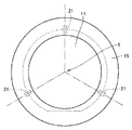
図10は、本発明によるクランプリングの第2の変形例を示す平面模式図である。図10を参照して、本発明によるクランプリングの第2の変形例を説明する。 FIG. 10 is a schematic plan view showing a second modification of the clamp ring according to the present invention. A second modification of the clamp ring according to the present invention will be described with reference to FIG.
図1〜図3に示したスパッタリング装置1に設置されたクランプリング15では、回動部材21がクランプリング15の中心から見て対向する位置に2つ配置されていた。しかし、図10に示すように、回動部材21の設置数は、3つでもよく、また4以上の複数でもよい。また、1つだけ回動部材21をクランプリング15に設置するようにしてもよい。
In the
また、複数の(たとえば3つの)回動部材21をクランプリング15に設置する場合には、図10に示すように、クランプリング15の中心点5から見て互いに等間隔となる位置にそれぞれ回動部材21を設置することが好ましい。このようにすれば、図8に示したように回動部材21の先端部26によりウェハ11の端部を押圧してクランプリング15とウェハ11とを分離する際に、ウェハ11に対して均等に力を加えることができる。この結果、クランプリング15からウェハ11をより確実に分離することができる。
Further, when a plurality of (for example, three) rotating
上述した本発明によるクランプリング15の特徴的な構成を要約すれば、本発明によるクランプ部材としてのクランプリング15は、基板(ウェハ11)に対する処理を行なう際に基板(ウェハ11)を保持するクランプリング15であって、ウェハ11を保持するための保持部としての内周側フランジ部3と、内周側フランジ部3に配置された回転軸22と、回動部材21とを備える。回動部材21は、回転軸22を中心として回転可能であり、一方端部としての先端部26と他方端部としての後端部27とを有する。回動部材21は、内周側フランジ部3がウェハ11を保持しているときにウェハ11の一部と間隔を隔てて重なる位置に先端部26が位置するように配置される。回動部材21は、内周側フランジ部3のクランプ部29がウェハ11を保持しているときに、後端部27を内周側フランジ部3に向けて押圧することにより回転軸22を中心として回転した結果、先端部26がウェハ11の一部(端部)を内周側フランジ部3から離れる方向に押圧することが可能である。なお、クランプリング15の内周側フランジ部3には、回転軸22の一部(端部)を収納する凹部が形成されていてもよく、回転軸22は押圧部材としての押え板23により内周側フランジ部3に押圧固定されていてもよい。この押え板23は固定部材としてのネジ24により内周側フランジ部3に固定されていてもよい。
To summarize the above-described characteristic configuration of the
このようにすれば、クランプリング15に回動部材21を設置するという比較的単純な機構部を設置することにより、内周側フランジ部3のクランプ部29により押圧、保持されたウェハ11をクランプリング15から分離する際に、回動部材21の先端部26によりウェハ11の一部を押圧できるので、ウェハ11をクランプリング15の内周側フランジ部3から確実に分離することができる。
In this way, by installing a relatively simple mechanism part in which the
また、内周側フランジ部3がウェハ11を保持しているときに、図6に示すように回動部材21の先端部26はウェハ11の一部と間隔を隔てた位置に配置される(ウェハ11と回動部材21とは接触していない)ので、内周側フランジ部3に保持されたウェハ11に対して処理(たとえばスパッタリングによる成膜処理)を行なっても、回動部材21の先端部26とウェハ11とが当該処理に起因して固着する(回動部材21の先端部26とウェハ11との表面上に連続する膜が形成され、その膜により回動部材21とウェハ11とが固着する)可能性を低減できる。
Further, when the inner
このため、本発明によるクランプリング15に保持されたウェハ11にスパッタリングなどの成膜処理を行なった後、クランプリング15からウェハ11が分離できないといった問題の発生確率を低減できる。この結果、クランプリング15からウェハ11が分離できないことにより、ウェハ11に対する処理を行なう処理装置としてのスパッタリング装置1の稼働率が低下する可能性を低減できる。また、上記のようにクランプリング15からウェハ11を分離できない場合、スパッタリング装置1の作動を停止して、当該ウェハ11をクランプリング15から作業員の手作業などで除去すると、そのウェハ11の表面状態などによっては当該ウェハ11を廃却処理しなければならないことがあるが、本発明によるクランプリング15を用いればこのような手作業によるウェハ11の除去を行なう可能性を低減できるので、結果的に廃却されるウェハ11の数を少なくできる(ウェハ11の歩留りを向上させることができる)。
Therefore, it is possible to reduce the probability of occurrence of a problem that the
また、回動部材21は上述のように内周側フランジ部3のクランプ部29がウェハ11を保持しているときにはウェハ11と接触していないので、ウェハ11へスパッタリングなどの成膜処理を行なっているときに回動部材21が動いたりしても、その回動部材21の動きに起因してウェハ11が振動する可能性を低減できる。このため、ウェハ11の振動に伴う異物の発生などの確率を低減できるので、このような異物に起因して、処理されたウェハ11の品質(たとえば形成された膜の膜質)が劣化する可能性を低減できる。
Further, since the rotating
上記クランプリング15では、内周側フランジ部3においてウェハ11と対向する面には凹部25が形成されていてもよい。内周側フランジ部3の凹部25に回動部材21が配置されていてもよい。この場合、回動部材21が設置されていない内周側フランジ部3の占有体積と比べた場合の、内周側フランジ部3に回動部材21を設置した場合の内周側フランジ部3の占有体積の増加割合を小さくすることができる。このため、クランプリング15が設置されるスパッタリング装置1などの処理装置の構造を特に変更することなく、本発明によるクランプリング15を処理装置に設置することができる。
In the
上記クランプリング15において、回動部材21を構成する材料は、ステンレス合金、および線膨張係数の値が鉄の線膨張係数の値以下である材料(低線膨張係数材料とも言う)からなる群から選択される1つを含んでいてもよい。このとき、クランプリング15に保持されたウェハ11に対して処理を行なう際に当該ウェハ11を加熱する必要がある場合、クランプリング15の温度も上昇する。その場合、回動部材21を上述のような材料により構成しておけば、クランプリング15の温度上昇に伴い回動部材21の温度が上昇しても、回動部材21の形状を安定させることができる(熱膨張による回動部材21の変形の程度を小さくできる)。この結果、回動部材21が変形して正常に動作しない(回転軸22を中心とした回転運動ができない)といった問題の発生確率を低減できる。
In the
なお、低線膨張係数材料としては、たとえばクランプリング15が用いられる温度領域(たとえば20°以上800℃以下という温度範囲)において鉄より線膨張係数が小さい材料を用いることができる。たとえば、低線膨張係数材料として、チタン、タンタル、タングステンなどの高融点金属、白金、炭素などを用いることができる。
As the low linear expansion coefficient material, for example, a material having a smaller linear expansion coefficient than iron in a temperature region (for example, a temperature range of 20 ° to 800 ° C.) in which the
上記クランプリング15において、内周側フランジ部3の表面には、内周側フランジ部3に保持されるウェハ11の表面に沿って、回動部材21が配置された領域から外側へ(ウェハ11の中央部側へ)突出する凸部33が形成されていてもよい。この場合、ウェハ11に対するスパッタリングなどの処理を行なう場合、当該処理の影響がクランプリング15とウェハ11との接触部18(図6参照)やクランプリング15の回動部材21にまで及ぶ(たとえば、処理としてスパッタリングなどの成膜処理を行なう場合、膜が上記接触部18や回動部材21表面にも形成される)可能性を低減できる。
In the
上記クランプリング15において、図9に示すように回動部材21の表面には表面処理層31が形成されていてもよい。この場合、表面処理層31を形成することで、回動部材21のベース(基体32)を構成する材料とは異なる材料層(表面処理層31)を回動部材21の表面に形成できる。このため、表面処理層31を構成する材料を適宜選択することにより、回動部材21の耐久性などの特性を改善することができる。たとえば、表面処理層31として窒化処理層などの耐磨耗性に優れた材料からなる層を形成すれば、回動部材21の摩耗の程度を低減できる。この結果、回動部材21の寿命を延長することができる。
In the
上記クランプリング15における、回動部材21において回転軸22と嵌合する部分には、回転軸22に沿って延び、回転軸22を内部に配置するための溝28が形成されていてもよい。回転軸22の延びる方向と交差する方向における溝28の底部の断面形状は三角形状であってもよい。この場合、溝28の底部の壁面が平坦な平面により構成されるので、回動部材21を製造する際に当該溝28を容易に形成できる。
A
この発明に従った成膜装置としてのスパッタリング装置1は、上記クランプリング15を備える。この場合、成膜処理としてのスパッタリング工程(S40)によりクランプリング15と基板(ウェハ11)とが固着したような場合であっても、回動部材21を用いて容易に基板(ウェハ11)とクランプリング15とを分離することができる。
A sputtering apparatus 1 as a film forming apparatus according to the present invention includes the
この発明に従った成膜方法では、以下の工程を実施する。まず、上記クランプ部材を用いて基板としてのウェハ11を保持する工程(クランプリング15とウェハ11とを接触させる工程(S20))を実施する。保持されたウェハ11の表面に膜を形成する成膜工程(スパッタリング工程(S40))を実施する。成膜工程(スパッタリング工程(S40))の終了後、クランプリング15の回動部材21における他方端部(後端部27)を保持部(内周側フランジ部3)に向けて押圧し、回転軸22を中心として回動部材21を回転させて、回動部材21の一方端部(先端部26)によりウェハ11の一部(端部)を押圧することにより、クランプリング15の内周側フランジ部3からウェハ11を分離する工程(ウェハとクランプリングを分離する工程(S51))を実施する。
In the film forming method according to the present invention, the following steps are performed. First, a step of holding the
この場合、クランプリング15の保持部(内周側フランジ部3)からウェハ11を分離する工程において、回動部材21の一方端部(先端部26)によりウェハ11の一部を押圧できる。このため、ウェハ11をクランプリング15の保持部(内周側フランジ部3)から確実に分離することができる。また、保持部(内周側フランジ部3)がウェハ11を保持しているときに、回動部材21の一方端部(先端部26)はウェハ11の一部(端部)と間隔を隔てた位置に配置される(ウェハ11と回動部材21とは接触していない)ので、保持部(内周側フランジ部3)に保持されたウェハ11に対して成膜工程(スパッタリング工程(S40))を行なっても、回動部材21の一方端部(先端部26)とウェハ11とが成膜工程の成膜処理(スパッタリング)に起因して、回動部材21の一方端部(先端部26)とウェハ11とに連続する膜が形成され、その膜により回動部材21とウェハ11とが固着する可能性を低減できる。
In this case, in the step of separating the
このため、基板を分離する工程(ウェハとクランプリングとを分離する工程(S51))において、クランプリング15からウェハ11が分離できないといった問題の発生確率を低減できる。この結果、クランプリング15からウェハ11が分離できないことにより、ウェハ11に対する処理を行なう処理装置としてのスパッタリング装置1の稼働率が低下する可能性を低減できる。
For this reason, it is possible to reduce the probability of occurrence of a problem that the
また、上記のようにクランプリング15からウェハ11が分離できない場合、スパッタリング装置1の作動を停止して、当該ウェハ11をクランプリング15から作業員の手作業などで除去すると、当該ウェハ11の表面状態などによっては当該ウェハ11を廃却処理しなければならないことがある。しかし、本発明によるクランプリング15を用いればこのような手作業によるウェハ11の除去が必要となる可能性を低減できるので、結果的に廃却されるウェハ11の数を少なくできる(ウェハ11および当該ウェハ11を用いる半導体装置の歩留りを向上させることができる)。
If the
また、回動部材21は上述のように保持部(内周側フランジ部3)がウェハ11を保持しているときにはウェハ11と接触していないので、ウェハ11へスパッタリング処理を行なっているときに回動部材21が動いたりしても、その回動部材21の動きに起因してウェハ11が振動する可能性を低減できる。このため、ウェハ11の振動に伴う異物の発生などの確率を低減できるので、このような異物に起因して、ウェハ11に形成された膜の膜質が劣化する可能性を低減できる。
Further, since the rotating
この発明に従った半導体装置の製造方法は、上記成膜方法を用いた半導体装置の製造方法であって、基板(ウェハ11)は半導体基板(例えばシリコン基板)であり、成膜工程(スパッタリング工程(S40))ではスパッタリング法を用いて膜を形成する。この場合、半導体装置の製造工程に、本発明による成膜方法を容易に適用できる。 A method for manufacturing a semiconductor device according to the present invention is a method for manufacturing a semiconductor device using the film forming method, wherein the substrate (wafer 11) is a semiconductor substrate (for example, a silicon substrate), and a film forming step (sputtering step). In (S40), a film is formed by sputtering. In this case, the film forming method according to the present invention can be easily applied to the manufacturing process of the semiconductor device.
今回開示された実施の形態はすべての点で例示であって制限的なものではないと考えられるべきである。本発明の範囲は上記した実施の形態ではなくて特許請求の範囲によって示され、特許請求の範囲と均等の意味および範囲内でのすべての変更が含まれることが意図される。 The embodiment disclosed this time should be considered as illustrative in all points and not restrictive. The scope of the present invention is shown not by the above-described embodiment but by the scope of claims, and is intended to include all modifications within the meaning and scope equivalent to the scope of claims.
1 スパッタリング装置、3 内周側フランジ部、5 中心点、7 開口部、8 側壁、9,19,20,30,34 矢印、10 リフター、11 ウェハ、12 ターゲット材、13 ロアーシールド体、14 蓋部材、15 クランプリング、16 ステージ、17 ベース部、18 接触部、21 回動部材、22 回転軸、23 押え板、24 ネジ、25 凹部、26 先端部、27 後端部、28 溝、29 クランプ部、31 表面処理層、32 基体、33 凸部。
DESCRIPTION OF SYMBOLS 1 Sputtering device, 3 Inner peripheral side flange part, 5 Center point, 7 Opening part, 8 Side wall, 9, 19, 20, 30, 34 Arrow, 10 Lifter, 11 Wafer, 12 Target material, 13 Lower shield body, 14 Lid Member, 15 Clamp ring, 16 Stage, 17 Base part, 18 Contact part, 21 Rotating member, 22 Rotating shaft, 23 Presser plate, 24 Screw, 25 Recessed part, 26 Tip part, 27 Rear end part, 28 Groove, 29 Clamp Part, 31 surface treatment layer, 32 base, 33 convex part.
Claims (9)
基板を保持するための保持部と、
前記保持部に配置された回転軸と、
前記回転軸を中心として回転可能な、一方端部と他方端部とを有する回動部材とを備え、
前記回動部材は、前記保持部が前記基板を保持しているときに前記基板の一部と間隔を隔てて重なる位置に前記一方端部が位置するように配置され、
前記回動部材は、前記保持部が前記基板を保持しているときに、前記他方端部を前記保持部に向けて押圧することにより前記回転軸を中心として回転した結果、前記一方端部が前記基板の一部を前記保持部から離れる方向に押圧することが可能である、クランプ部材。 A clamp member for holding the substrate when processing the substrate,
A holding unit for holding the substrate;
A rotating shaft disposed in the holding portion;
A rotating member having a first end and a second end that is rotatable about the rotation axis;
The rotating member is arranged so that the one end portion is located at a position overlapping with a part of the substrate with a gap when the holding portion holds the substrate.
The rotating member rotates around the rotation axis by pressing the other end portion toward the holding portion when the holding portion holds the substrate. A clamp member capable of pressing a part of the substrate in a direction away from the holding portion.
前記保持部の凹部に前記回動部材は配置されている、請求項1に記載のクランプ部材。 A concave portion is formed on the surface of the holding portion facing the substrate,
The clamp member according to claim 1, wherein the rotating member is disposed in the concave portion of the holding portion.
前記回転軸の延びる方向と交差する方向における前記溝の底部の断面形状は三角形状である、請求項1〜5のいずれか1項に記載のクランプ部材。 In the rotating member, a portion that fits the rotating shaft is formed with a groove that extends along the rotating shaft and is disposed inside the rotating shaft.
The clamp member according to any one of claims 1 to 5, wherein a cross-sectional shape of a bottom portion of the groove in a direction intersecting with a direction in which the rotation axis extends is a triangular shape.
前記保持された基板の表面に膜を形成する成膜工程と、
前記成膜工程の終了後、前記クランプ部材の前記回動部材における前記他方端部を前記保持部に向けて押圧し、前記回転軸を中心として前記回動部材を回転させて、前記回動部材の前記一方端部により前記基板の一部を押圧することにより、前記クランプ部材の前記保持部から前記基板を分離する工程とを備える、成膜方法。 A step of holding the substrate using the clamp member according to claim 1;
A film forming step of forming a film on the surface of the held substrate;
After the film formation step, the other end portion of the rotating member of the clamp member is pressed toward the holding portion, the rotating member is rotated about the rotating shaft, and the rotating member Separating the substrate from the holding portion of the clamp member by pressing a part of the substrate with the one end of the film.
前記基板は半導体基板であり、
前記成膜工程ではスパッタリング法を用いて前記膜を形成する、半導体装置の製造方法。 A method of manufacturing a semiconductor device using the film forming method according to claim 8,
The substrate is a semiconductor substrate;
A method for manufacturing a semiconductor device, wherein the film is formed by a sputtering method in the film forming step.
Priority Applications (2)
| Application Number | Priority Date | Filing Date | Title |
|---|---|---|---|
| JP2004151953A JP2005333063A (en) | 2004-05-21 | 2004-05-21 | Clamp member, film forming device, film forming method, and method for manufacturing semiconductor device |
| US11/133,452 US20050257746A1 (en) | 2004-05-21 | 2005-05-20 | Clamp member, film deposition apparatus, film deposition method, and semiconductor device manufacturing method |
Applications Claiming Priority (1)
| Application Number | Priority Date | Filing Date | Title |
|---|---|---|---|
| JP2004151953A JP2005333063A (en) | 2004-05-21 | 2004-05-21 | Clamp member, film forming device, film forming method, and method for manufacturing semiconductor device |
Publications (2)
| Publication Number | Publication Date |
|---|---|
| JP2005333063A true JP2005333063A (en) | 2005-12-02 |
| JP2005333063A5 JP2005333063A5 (en) | 2007-06-21 |
Family
ID=35373981
Family Applications (1)
| Application Number | Title | Priority Date | Filing Date |
|---|---|---|---|
| JP2004151953A Withdrawn JP2005333063A (en) | 2004-05-21 | 2004-05-21 | Clamp member, film forming device, film forming method, and method for manufacturing semiconductor device |
Country Status (2)
| Country | Link |
|---|---|
| US (1) | US20050257746A1 (en) |
| JP (1) | JP2005333063A (en) |
Cited By (2)
| Publication number | Priority date | Publication date | Assignee | Title |
|---|---|---|---|---|
| JP2010225740A (en) * | 2009-03-23 | 2010-10-07 | Tokyo Electron Ltd | Substrate processing method, and substrate processing apparatus |
| KR20190090690A (en) | 2018-01-25 | 2019-08-02 | 에이블릭 가부시키가이샤 | Semiconductor manufacturing apparatus and film formation method of semiconductor device |
Families Citing this family (5)
| Publication number | Priority date | Publication date | Assignee | Title |
|---|---|---|---|---|
| TWI470110B (en) * | 2012-09-07 | 2015-01-21 | Manz Taiwan Ltd | Clamping device for chemical deposition equipment |
| JP6870531B2 (en) * | 2017-08-21 | 2021-05-12 | 三菱電機株式会社 | Power module and power converter |
| CN107937881B (en) * | 2017-11-20 | 2019-07-05 | 深圳市华星光电半导体显示技术有限公司 | Substrate clamping device |
| US20220157635A1 (en) * | 2020-11-18 | 2022-05-19 | Applied Materials, Inc. | Thin substrate handling via edge clamping |
| CN113903649B (en) * | 2021-09-23 | 2024-04-12 | 北京北方华创微电子装备有限公司 | Semiconductor processing equipment |
Family Cites Families (7)
| Publication number | Priority date | Publication date | Assignee | Title |
|---|---|---|---|---|
| US5513594A (en) * | 1993-10-20 | 1996-05-07 | Mcclanahan; Adolphus E. | Clamp with wafer release for semiconductor wafer processing equipment |
| US5437757A (en) * | 1994-01-21 | 1995-08-01 | Applied Materials, Inc. | Clamp ring for domed pedestal in wafer processing chamber |
| DE4420050C1 (en) * | 1994-06-08 | 1995-08-24 | Weidmueller Interface | Electrical insulation hand-held stripping tool for conductor ends |
| JP3471543B2 (en) * | 1996-11-07 | 2003-12-02 | 大日本スクリーン製造株式会社 | Rotary substrate drying equipment |
| US5922133A (en) * | 1997-09-12 | 1999-07-13 | Applied Materials, Inc. | Multiple edge deposition exclusion rings |
| US6699375B1 (en) * | 2000-06-29 | 2004-03-02 | Applied Materials, Inc. | Method of extending process kit consumable recycling life |
| JP4488646B2 (en) * | 2001-04-23 | 2010-06-23 | 株式会社トプコン | Wafer holding device |
-
2004
- 2004-05-21 JP JP2004151953A patent/JP2005333063A/en not_active Withdrawn
-
2005
- 2005-05-20 US US11/133,452 patent/US20050257746A1/en not_active Abandoned
Cited By (2)
| Publication number | Priority date | Publication date | Assignee | Title |
|---|---|---|---|---|
| JP2010225740A (en) * | 2009-03-23 | 2010-10-07 | Tokyo Electron Ltd | Substrate processing method, and substrate processing apparatus |
| KR20190090690A (en) | 2018-01-25 | 2019-08-02 | 에이블릭 가부시키가이샤 | Semiconductor manufacturing apparatus and film formation method of semiconductor device |
Also Published As
| Publication number | Publication date |
|---|---|
| US20050257746A1 (en) | 2005-11-24 |
Similar Documents
| Publication | Publication Date | Title |
|---|---|---|
| JP4358108B2 (en) | A set of instruments for loading, supporting and removing in a coating apparatus | |
| JP5001432B2 (en) | Substrate processing apparatus and substrate processing method | |
| JP3955532B2 (en) | Wet processing of workpieces | |
| TWI570835B (en) | Two piece shutter disk assembly for a substrate process chamber | |
| TW202003892A (en) | Pre-clean chamber with integrated shutter garage | |
| JP2005333063A (en) | Clamp member, film forming device, film forming method, and method for manufacturing semiconductor device | |
| JP6513048B2 (en) | Liquid processing device | |
| TWI829685B (en) | Two piece shutter disk assembly with self-centering feature | |
| TW201407713A (en) | Holding mechanism of substrate retaining ring | |
| JP4101524B2 (en) | Deposition equipment | |
| JP2010013707A (en) | Sputtering apparatus | |
| JP2007190593A (en) | Substrate holding device and substrate working device | |
| JP2005077845A (en) | Sputtering system, method for manufacturing substrate with thin film, method for manufacturing mask blank, and method for manufacturing the transfer mask | |
| JP2000306982A (en) | Wafer side conversion holder and method for retaining wafer using the same | |
| EP3361496A1 (en) | Heat treatment vessel for single-crystal silicon carbide substrate and etching method | |
| JP4539981B2 (en) | Substrate holding device | |
| JP2003282680A (en) | Board lifer, clamp ring, and board processing device | |
| JP2003197716A (en) | Substrate support and semiconductor production unit | |
| JP2001181845A (en) | Film deposition system | |
| JP2001181845A5 (en) | Film forming apparatus and method of processing target object | |
| JP7038013B2 (en) | Board support mechanism | |
| JP4441158B2 (en) | Board holder | |
| JP2006186023A (en) | Wafer holder and wafer transporter | |
| JP2009200390A (en) | Probe card transfer apparatus | |
| JP2008075180A (en) | Substrate holder assembly device |
Legal Events
| Date | Code | Title | Description |
|---|---|---|---|
| A521 | Written amendment |
Free format text: JAPANESE INTERMEDIATE CODE: A523 Effective date: 20070508 |
|
| A621 | Written request for application examination |
Free format text: JAPANESE INTERMEDIATE CODE: A621 Effective date: 20070508 |
|
| A761 | Written withdrawal of application |
Free format text: JAPANESE INTERMEDIATE CODE: A761 Effective date: 20090226 |