JP2005294818A - 半導体装置 - Google Patents
半導体装置 Download PDFInfo
- Publication number
- JP2005294818A JP2005294818A JP2005063905A JP2005063905A JP2005294818A JP 2005294818 A JP2005294818 A JP 2005294818A JP 2005063905 A JP2005063905 A JP 2005063905A JP 2005063905 A JP2005063905 A JP 2005063905A JP 2005294818 A JP2005294818 A JP 2005294818A
- Authority
- JP
- Japan
- Prior art keywords
- insulating film
- antenna
- substrate
- integrated circuit
- film
- Prior art date
- Legal status (The legal status is an assumption and is not a legal conclusion. Google has not performed a legal analysis and makes no representation as to the accuracy of the status listed.)
- Granted
Links
- 239000004065 semiconductor Substances 0.000 title claims abstract description 147
- 239000000758 substrate Substances 0.000 claims abstract description 146
- 239000000696 magnetic material Substances 0.000 claims abstract description 31
- 239000010419 fine particle Substances 0.000 claims abstract description 29
- 239000010408 film Substances 0.000 claims description 367
- 238000000034 method Methods 0.000 claims description 110
- 239000004020 conductor Substances 0.000 claims description 62
- 239000011347 resin Substances 0.000 claims description 42
- 229920005989 resin Polymers 0.000 claims description 42
- 239000000463 material Substances 0.000 claims description 40
- 238000007639 printing Methods 0.000 claims description 14
- 239000010409 thin film Substances 0.000 claims description 14
- 238000007772 electroless plating Methods 0.000 claims description 4
- 238000009713 electroplating Methods 0.000 claims description 3
- 230000002708 enhancing effect Effects 0.000 abstract description 4
- 238000009413 insulation Methods 0.000 abstract 1
- 239000010410 layer Substances 0.000 description 76
- 239000011229 interlayer Substances 0.000 description 54
- 239000012535 impurity Substances 0.000 description 36
- 239000007789 gas Substances 0.000 description 34
- 229910052814 silicon oxide Inorganic materials 0.000 description 34
- 239000000853 adhesive Substances 0.000 description 33
- 230000001070 adhesive effect Effects 0.000 description 33
- 238000004519 manufacturing process Methods 0.000 description 31
- 229910052581 Si3N4 Inorganic materials 0.000 description 28
- HQVNEWCFYHHQES-UHFFFAOYSA-N silicon nitride Chemical compound N12[Si]34N5[Si]62N3[Si]51N64 HQVNEWCFYHHQES-UHFFFAOYSA-N 0.000 description 28
- 238000005530 etching Methods 0.000 description 25
- VYPSYNLAJGMNEJ-UHFFFAOYSA-N Silicium dioxide Chemical compound O=[Si]=O VYPSYNLAJGMNEJ-UHFFFAOYSA-N 0.000 description 24
- 239000011521 glass Substances 0.000 description 22
- 229910052751 metal Inorganic materials 0.000 description 19
- 239000002184 metal Substances 0.000 description 19
- 239000001257 hydrogen Substances 0.000 description 17
- 229910052739 hydrogen Inorganic materials 0.000 description 17
- 238000002955 isolation Methods 0.000 description 17
- 238000000926 separation method Methods 0.000 description 17
- UFHFLCQGNIYNRP-UHFFFAOYSA-N Hydrogen Chemical compound [H][H] UFHFLCQGNIYNRP-UHFFFAOYSA-N 0.000 description 16
- XUIMIQQOPSSXEZ-UHFFFAOYSA-N Silicon Chemical compound [Si] XUIMIQQOPSSXEZ-UHFFFAOYSA-N 0.000 description 16
- 229910052710 silicon Inorganic materials 0.000 description 16
- 239000010703 silicon Substances 0.000 description 16
- 239000002585 base Substances 0.000 description 15
- KPUWHANPEXNPJT-UHFFFAOYSA-N disiloxane Chemical class [SiH3]O[SiH3] KPUWHANPEXNPJT-UHFFFAOYSA-N 0.000 description 15
- 229910045601 alloy Inorganic materials 0.000 description 12
- 239000000956 alloy Substances 0.000 description 12
- 239000013078 crystal Substances 0.000 description 12
- 150000002736 metal compounds Chemical class 0.000 description 12
- 230000015572 biosynthetic process Effects 0.000 description 11
- 238000005268 plasma chemical vapour deposition Methods 0.000 description 11
- 230000008569 process Effects 0.000 description 11
- IJGRMHOSHXDMSA-UHFFFAOYSA-N Atomic nitrogen Chemical compound N#N IJGRMHOSHXDMSA-UHFFFAOYSA-N 0.000 description 10
- 230000015654 memory Effects 0.000 description 10
- PXHVJJICTQNCMI-UHFFFAOYSA-N nickel Substances [Ni] PXHVJJICTQNCMI-UHFFFAOYSA-N 0.000 description 8
- 238000000059 patterning Methods 0.000 description 8
- 230000001681 protective effect Effects 0.000 description 8
- 230000002829 reductive effect Effects 0.000 description 8
- 229910021332 silicide Inorganic materials 0.000 description 8
- FVBUAEGBCNSCDD-UHFFFAOYSA-N silicide(4-) Chemical compound [Si-4] FVBUAEGBCNSCDD-UHFFFAOYSA-N 0.000 description 8
- 239000002356 single layer Substances 0.000 description 8
- 239000010936 titanium Substances 0.000 description 8
- 239000004642 Polyimide Substances 0.000 description 7
- 238000002425 crystallisation Methods 0.000 description 7
- -1 fluorine halide Chemical class 0.000 description 7
- 239000012212 insulator Substances 0.000 description 7
- 229910052759 nickel Inorganic materials 0.000 description 7
- 238000000206 photolithography Methods 0.000 description 7
- 239000004033 plastic Substances 0.000 description 7
- 229920003023 plastic Polymers 0.000 description 7
- 229920001721 polyimide Polymers 0.000 description 7
- 125000001424 substituent group Chemical group 0.000 description 7
- 230000008901 benefit Effects 0.000 description 6
- 229910052802 copper Inorganic materials 0.000 description 6
- 238000010438 heat treatment Methods 0.000 description 6
- 238000005499 laser crystallization Methods 0.000 description 6
- 239000005022 packaging material Substances 0.000 description 6
- 239000011241 protective layer Substances 0.000 description 6
- 238000004544 sputter deposition Methods 0.000 description 6
- 239000004952 Polyamide Substances 0.000 description 5
- 229910052783 alkali metal Inorganic materials 0.000 description 5
- 150000001340 alkali metals Chemical class 0.000 description 5
- 229910052784 alkaline earth metal Inorganic materials 0.000 description 5
- 150000001342 alkaline earth metals Chemical class 0.000 description 5
- 229910052804 chromium Inorganic materials 0.000 description 5
- 230000007547 defect Effects 0.000 description 5
- 230000004907 flux Effects 0.000 description 5
- 230000006870 function Effects 0.000 description 5
- 229910052742 iron Inorganic materials 0.000 description 5
- 229910044991 metal oxide Inorganic materials 0.000 description 5
- 150000004706 metal oxides Chemical class 0.000 description 5
- 229910052757 nitrogen Inorganic materials 0.000 description 5
- 230000010355 oscillation Effects 0.000 description 5
- 229920002647 polyamide Polymers 0.000 description 5
- 229910052718 tin Inorganic materials 0.000 description 5
- 229910052719 titanium Inorganic materials 0.000 description 5
- XKRFYHLGVUSROY-UHFFFAOYSA-N Argon Chemical compound [Ar] XKRFYHLGVUSROY-UHFFFAOYSA-N 0.000 description 4
- 229910004298 SiO 2 Inorganic materials 0.000 description 4
- NIXOWILDQLNWCW-UHFFFAOYSA-N acrylic acid group Chemical group C(C=C)(=O)O NIXOWILDQLNWCW-UHFFFAOYSA-N 0.000 description 4
- 230000002411 adverse Effects 0.000 description 4
- 229910021417 amorphous silicon Inorganic materials 0.000 description 4
- 230000004888 barrier function Effects 0.000 description 4
- 230000003197 catalytic effect Effects 0.000 description 4
- 125000001153 fluoro group Chemical group F* 0.000 description 4
- 229910052736 halogen Inorganic materials 0.000 description 4
- 238000005984 hydrogenation reaction Methods 0.000 description 4
- 229910052750 molybdenum Inorganic materials 0.000 description 4
- 125000000962 organic group Chemical group 0.000 description 4
- JMANVNJQNLATNU-UHFFFAOYSA-N oxalonitrile Chemical compound N#CC#N JMANVNJQNLATNU-UHFFFAOYSA-N 0.000 description 4
- 238000002161 passivation Methods 0.000 description 4
- 239000004925 Acrylic resin Substances 0.000 description 3
- 229910004205 SiNX Inorganic materials 0.000 description 3
- ATJFFYVFTNAWJD-UHFFFAOYSA-N Tin Chemical compound [Sn] ATJFFYVFTNAWJD-UHFFFAOYSA-N 0.000 description 3
- 230000001133 acceleration Effects 0.000 description 3
- 125000000217 alkyl group Chemical group 0.000 description 3
- 238000000137 annealing Methods 0.000 description 3
- 150000004945 aromatic hydrocarbons Chemical class 0.000 description 3
- 238000004380 ashing Methods 0.000 description 3
- 239000000460 chlorine Substances 0.000 description 3
- 238000009826 distribution Methods 0.000 description 3
- 239000001307 helium Substances 0.000 description 3
- 229910052734 helium Inorganic materials 0.000 description 3
- SWQJXJOGLNCZEY-UHFFFAOYSA-N helium atom Chemical compound [He] SWQJXJOGLNCZEY-UHFFFAOYSA-N 0.000 description 3
- 230000001678 irradiating effect Effects 0.000 description 3
- 238000004518 low pressure chemical vapour deposition Methods 0.000 description 3
- 125000004433 nitrogen atom Chemical group N* 0.000 description 3
- 125000004430 oxygen atom Chemical group O* 0.000 description 3
- 229910052698 phosphorus Inorganic materials 0.000 description 3
- 238000004528 spin coating Methods 0.000 description 3
- 229910052721 tungsten Inorganic materials 0.000 description 3
- 229910052725 zinc Inorganic materials 0.000 description 3
- 229920000178 Acrylic resin Polymers 0.000 description 2
- 229910018125 Al-Si Inorganic materials 0.000 description 2
- 229910018520 Al—Si Inorganic materials 0.000 description 2
- ZOXJGFHDIHLPTG-UHFFFAOYSA-N Boron Chemical compound [B] ZOXJGFHDIHLPTG-UHFFFAOYSA-N 0.000 description 2
- OKTJSMMVPCPJKN-UHFFFAOYSA-N Carbon Chemical compound [C] OKTJSMMVPCPJKN-UHFFFAOYSA-N 0.000 description 2
- 239000004593 Epoxy Substances 0.000 description 2
- 229910017060 Fe Cr Inorganic materials 0.000 description 2
- 229910002544 Fe-Cr Inorganic materials 0.000 description 2
- 229910003271 Ni-Fe Inorganic materials 0.000 description 2
- OAICVXFJPJFONN-UHFFFAOYSA-N Phosphorus Chemical compound [P] OAICVXFJPJFONN-UHFFFAOYSA-N 0.000 description 2
- 239000004696 Poly ether ether ketone Substances 0.000 description 2
- 239000004697 Polyetherimide Substances 0.000 description 2
- 229910000577 Silicon-germanium Inorganic materials 0.000 description 2
- 229910002796 Si–Al Inorganic materials 0.000 description 2
- 229910002808 Si–O–Si Inorganic materials 0.000 description 2
- 229910001035 Soft ferrite Inorganic materials 0.000 description 2
- BOTDANWDWHJENH-UHFFFAOYSA-N Tetraethyl orthosilicate Chemical compound CCO[Si](OCC)(OCC)OCC BOTDANWDWHJENH-UHFFFAOYSA-N 0.000 description 2
- LEVVHYCKPQWKOP-UHFFFAOYSA-N [Si].[Ge] Chemical compound [Si].[Ge] LEVVHYCKPQWKOP-UHFFFAOYSA-N 0.000 description 2
- 229910052782 aluminium Inorganic materials 0.000 description 2
- 239000005407 aluminoborosilicate glass Substances 0.000 description 2
- 229910052786 argon Inorganic materials 0.000 description 2
- 229910052785 arsenic Inorganic materials 0.000 description 2
- 239000012298 atmosphere Substances 0.000 description 2
- 125000004429 atom Chemical group 0.000 description 2
- 229910052788 barium Inorganic materials 0.000 description 2
- DSAJWYNOEDNPEQ-UHFFFAOYSA-N barium atom Chemical compound [Ba] DSAJWYNOEDNPEQ-UHFFFAOYSA-N 0.000 description 2
- 229910052796 boron Inorganic materials 0.000 description 2
- 239000005388 borosilicate glass Substances 0.000 description 2
- 239000002775 capsule Substances 0.000 description 2
- 229910052799 carbon Inorganic materials 0.000 description 2
- 238000006243 chemical reaction Methods 0.000 description 2
- UPHIPHFJVNKLMR-UHFFFAOYSA-N chromium iron Chemical compound [Cr].[Fe] UPHIPHFJVNKLMR-UHFFFAOYSA-N 0.000 description 2
- 238000004891 communication Methods 0.000 description 2
- 230000008025 crystallization Effects 0.000 description 2
- 238000000354 decomposition reaction Methods 0.000 description 2
- 230000005674 electromagnetic induction Effects 0.000 description 2
- 238000001704 evaporation Methods 0.000 description 2
- 229910052731 fluorine Inorganic materials 0.000 description 2
- 239000011737 fluorine Substances 0.000 description 2
- 229910052732 germanium Inorganic materials 0.000 description 2
- GNPVGFCGXDBREM-UHFFFAOYSA-N germanium atom Chemical compound [Ge] GNPVGFCGXDBREM-UHFFFAOYSA-N 0.000 description 2
- 229910052737 gold Inorganic materials 0.000 description 2
- 150000002367 halogens Chemical class 0.000 description 2
- 229910010272 inorganic material Inorganic materials 0.000 description 2
- 239000011147 inorganic material Substances 0.000 description 2
- 229910052743 krypton Inorganic materials 0.000 description 2
- DNNSSWSSYDEUBZ-UHFFFAOYSA-N krypton atom Chemical compound [Kr] DNNSSWSSYDEUBZ-UHFFFAOYSA-N 0.000 description 2
- 238000010030 laminating Methods 0.000 description 2
- 239000007788 liquid Substances 0.000 description 2
- 229910052754 neon Inorganic materials 0.000 description 2
- GKAOGPIIYCISHV-UHFFFAOYSA-N neon atom Chemical compound [Ne] GKAOGPIIYCISHV-UHFFFAOYSA-N 0.000 description 2
- 229910052758 niobium Inorganic materials 0.000 description 2
- 239000012299 nitrogen atmosphere Substances 0.000 description 2
- 238000007645 offset printing Methods 0.000 description 2
- 230000003287 optical effect Effects 0.000 description 2
- 239000011368 organic material Substances 0.000 description 2
- 229910052763 palladium Inorganic materials 0.000 description 2
- 229910000889 permalloy Inorganic materials 0.000 description 2
- 230000035699 permeability Effects 0.000 description 2
- 239000011574 phosphorus Substances 0.000 description 2
- 238000007747 plating Methods 0.000 description 2
- 229920002492 poly(sulfone) Polymers 0.000 description 2
- 229920001230 polyarylate Polymers 0.000 description 2
- 229920001707 polybutylene terephthalate Polymers 0.000 description 2
- 229920002530 polyetherether ketone Polymers 0.000 description 2
- 229920001601 polyetherimide Polymers 0.000 description 2
- 229920000139 polyethylene terephthalate Polymers 0.000 description 2
- 239000005020 polyethylene terephthalate Substances 0.000 description 2
- 239000010453 quartz Substances 0.000 description 2
- 238000007650 screen-printing Methods 0.000 description 2
- 229910052709 silver Inorganic materials 0.000 description 2
- 239000000243 solution Substances 0.000 description 2
- 239000002904 solvent Substances 0.000 description 2
- 229910052715 tantalum Inorganic materials 0.000 description 2
- MZLGASXMSKOWSE-UHFFFAOYSA-N tantalum nitride Chemical compound [Ta]#N MZLGASXMSKOWSE-UHFFFAOYSA-N 0.000 description 2
- 238000002230 thermal chemical vapour deposition Methods 0.000 description 2
- 229920001187 thermosetting polymer Polymers 0.000 description 2
- 229910000859 α-Fe Inorganic materials 0.000 description 2
- YCKRFDGAMUMZLT-UHFFFAOYSA-N Fluorine atom Chemical compound [F] YCKRFDGAMUMZLT-UHFFFAOYSA-N 0.000 description 1
- 229910005883 NiSi Inorganic materials 0.000 description 1
- 239000004677 Nylon Substances 0.000 description 1
- 229920012266 Poly(ether sulfone) PES Polymers 0.000 description 1
- 239000004743 Polypropylene Substances 0.000 description 1
- 239000004793 Polystyrene Substances 0.000 description 1
- 238000001237 Raman spectrum Methods 0.000 description 1
- 229910003902 SiCl 4 Inorganic materials 0.000 description 1
- 229910004286 SiNxOy Inorganic materials 0.000 description 1
- 229910020286 SiOxNy Inorganic materials 0.000 description 1
- GWEVSGVZZGPLCZ-UHFFFAOYSA-N Titan oxide Chemical compound O=[Ti]=O GWEVSGVZZGPLCZ-UHFFFAOYSA-N 0.000 description 1
- RTAQQCXQSZGOHL-UHFFFAOYSA-N Titanium Chemical compound [Ti] RTAQQCXQSZGOHL-UHFFFAOYSA-N 0.000 description 1
- 238000002441 X-ray diffraction Methods 0.000 description 1
- GDFCWFBWQUEQIJ-UHFFFAOYSA-N [B].[P] Chemical compound [B].[P] GDFCWFBWQUEQIJ-UHFFFAOYSA-N 0.000 description 1
- XECAHXYUAAWDEL-UHFFFAOYSA-N acrylonitrile butadiene styrene Chemical compound C=CC=C.C=CC#N.C=CC1=CC=CC=C1 XECAHXYUAAWDEL-UHFFFAOYSA-N 0.000 description 1
- 239000004676 acrylonitrile butadiene styrene Substances 0.000 description 1
- 229920000122 acrylonitrile butadiene styrene Polymers 0.000 description 1
- 150000001298 alcohols Chemical class 0.000 description 1
- PNEYBMLMFCGWSK-UHFFFAOYSA-N aluminium oxide Inorganic materials [O-2].[O-2].[O-2].[Al+3].[Al+3] PNEYBMLMFCGWSK-UHFFFAOYSA-N 0.000 description 1
- RQNWIZPPADIBDY-UHFFFAOYSA-N arsenic atom Chemical compound [As] RQNWIZPPADIBDY-UHFFFAOYSA-N 0.000 description 1
- 238000001505 atmospheric-pressure chemical vapour deposition Methods 0.000 description 1
- QVGXLLKOCUKJST-UHFFFAOYSA-N atomic oxygen Chemical compound [O] QVGXLLKOCUKJST-UHFFFAOYSA-N 0.000 description 1
- 230000002238 attenuated effect Effects 0.000 description 1
- 238000005452 bending Methods 0.000 description 1
- UMIVXZPTRXBADB-UHFFFAOYSA-N benzocyclobutene Chemical compound C1=CC=C2CCC2=C1 UMIVXZPTRXBADB-UHFFFAOYSA-N 0.000 description 1
- 239000003990 capacitor Substances 0.000 description 1
- 239000000969 carrier Substances 0.000 description 1
- 239000000919 ceramic Substances 0.000 description 1
- 238000005229 chemical vapour deposition Methods 0.000 description 1
- SLLGVCUQYRMELA-UHFFFAOYSA-N chlorosilicon Chemical compound Cl[Si] SLLGVCUQYRMELA-UHFFFAOYSA-N 0.000 description 1
- 238000004140 cleaning Methods 0.000 description 1
- 239000011248 coating agent Substances 0.000 description 1
- 238000000576 coating method Methods 0.000 description 1
- PMHQVHHXPFUNSP-UHFFFAOYSA-M copper(1+);methylsulfanylmethane;bromide Chemical compound Br[Cu].CSC PMHQVHHXPFUNSP-UHFFFAOYSA-M 0.000 description 1
- 238000010168 coupling process Methods 0.000 description 1
- 230000007423 decrease Effects 0.000 description 1
- 238000010586 diagram Methods 0.000 description 1
- 238000009792 diffusion process Methods 0.000 description 1
- 238000007865 diluting Methods 0.000 description 1
- 238000010790 dilution Methods 0.000 description 1
- 239000012895 dilution Substances 0.000 description 1
- 238000007598 dipping method Methods 0.000 description 1
- 238000007599 discharging Methods 0.000 description 1
- 230000000694 effects Effects 0.000 description 1
- 239000003822 epoxy resin Substances 0.000 description 1
- 239000000945 filler Substances 0.000 description 1
- 238000011049 filling Methods 0.000 description 1
- 235000013305 food Nutrition 0.000 description 1
- BHEPBYXIRTUNPN-UHFFFAOYSA-N hydridophosphorus(.) (triplet) Chemical compound [PH] BHEPBYXIRTUNPN-UHFFFAOYSA-N 0.000 description 1
- 150000002431 hydrogen Chemical class 0.000 description 1
- 230000006872 improvement Effects 0.000 description 1
- 239000011261 inert gas Substances 0.000 description 1
- 229910052748 manganese Inorganic materials 0.000 description 1
- 150000002739 metals Chemical class 0.000 description 1
- 229910021424 microcrystalline silicon Inorganic materials 0.000 description 1
- 238000002156 mixing Methods 0.000 description 1
- 239000000203 mixture Substances 0.000 description 1
- 230000004048 modification Effects 0.000 description 1
- 238000012986 modification Methods 0.000 description 1
- 229910021421 monocrystalline silicon Inorganic materials 0.000 description 1
- 229910021334 nickel silicide Inorganic materials 0.000 description 1
- RUFLMLWJRZAWLJ-UHFFFAOYSA-N nickel silicide Chemical compound [Ni]=[Si]=[Ni] RUFLMLWJRZAWLJ-UHFFFAOYSA-N 0.000 description 1
- 150000004767 nitrides Chemical class 0.000 description 1
- 229920001778 nylon Polymers 0.000 description 1
- 230000003647 oxidation Effects 0.000 description 1
- 238000007254 oxidation reaction Methods 0.000 description 1
- TWNQGVIAIRXVLR-UHFFFAOYSA-N oxo(oxoalumanyloxy)alumane Chemical compound O=[Al]O[Al]=O TWNQGVIAIRXVLR-UHFFFAOYSA-N 0.000 description 1
- 239000001301 oxygen Substances 0.000 description 1
- 229910052760 oxygen Inorganic materials 0.000 description 1
- 239000002245 particle Substances 0.000 description 1
- 238000009832 plasma treatment Methods 0.000 description 1
- 229920000636 poly(norbornene) polymer Polymers 0.000 description 1
- 239000004417 polycarbonate Substances 0.000 description 1
- 229920000515 polycarbonate Polymers 0.000 description 1
- 229910021420 polycrystalline silicon Inorganic materials 0.000 description 1
- 229920000647 polyepoxide Polymers 0.000 description 1
- 229920000728 polyester Polymers 0.000 description 1
- 239000011112 polyethylene naphthalate Substances 0.000 description 1
- 229920001155 polypropylene Polymers 0.000 description 1
- 229920002223 polystyrene Polymers 0.000 description 1
- 229920002689 polyvinyl acetate Polymers 0.000 description 1
- 239000011118 polyvinyl acetate Substances 0.000 description 1
- 239000004800 polyvinyl chloride Substances 0.000 description 1
- 229920000915 polyvinyl chloride Polymers 0.000 description 1
- 239000011148 porous material Substances 0.000 description 1
- 238000003672 processing method Methods 0.000 description 1
- 229910052706 scandium Inorganic materials 0.000 description 1
- 230000008054 signal transmission Effects 0.000 description 1
- 238000003980 solgel method Methods 0.000 description 1
- 238000005507 spraying Methods 0.000 description 1
- 239000010935 stainless steel Substances 0.000 description 1
- 229910001220 stainless steel Inorganic materials 0.000 description 1
- 239000007858 starting material Substances 0.000 description 1
- 239000000126 substance Substances 0.000 description 1
- 229920003002 synthetic resin Polymers 0.000 description 1
- 239000000057 synthetic resin Substances 0.000 description 1
- OGIDPMRJRNCKJF-UHFFFAOYSA-N titanium oxide Inorganic materials [Ti]=O OGIDPMRJRNCKJF-UHFFFAOYSA-N 0.000 description 1
- 230000007704 transition Effects 0.000 description 1
- JOHWNGGYGAVMGU-UHFFFAOYSA-N trifluorochlorine Chemical compound FCl(F)F JOHWNGGYGAVMGU-UHFFFAOYSA-N 0.000 description 1
- WFKWXMTUELFFGS-UHFFFAOYSA-N tungsten Chemical compound [W] WFKWXMTUELFFGS-UHFFFAOYSA-N 0.000 description 1
- 239000010937 tungsten Substances 0.000 description 1
- 238000001771 vacuum deposition Methods 0.000 description 1
- 229910052720 vanadium Inorganic materials 0.000 description 1
- 238000007740 vapor deposition Methods 0.000 description 1
- 239000002699 waste material Substances 0.000 description 1
- XLYOFNOQVPJJNP-UHFFFAOYSA-N water Substances O XLYOFNOQVPJJNP-UHFFFAOYSA-N 0.000 description 1
- 230000003313 weakening effect Effects 0.000 description 1
Images
Landscapes
- Internal Circuitry In Semiconductor Integrated Circuit Devices (AREA)
- Semiconductor Integrated Circuits (AREA)
- Thin Film Transistor (AREA)
- Recrystallisation Techniques (AREA)
Abstract
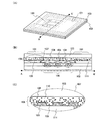
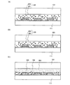
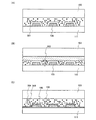
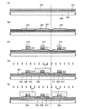
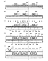
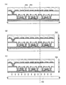
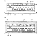
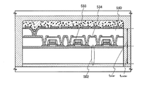
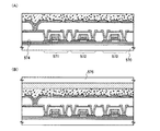
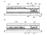
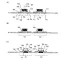
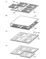
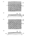
【解決手段】IDチップなどの半導体装置は、薄膜の半導体膜で形成された半導体素子が用いられた集積回路と、該集積回路に接続されたアンテナとを有する。アンテナ105は、集積回路と同じ基板上に一体形成されている方が、IDチップの機械的強度を高めることができるので望ましい。なおかつアンテナは、円状または螺旋状に巻かれた導線を有し、導線と導線の間に、軟磁性材料を用いた微粒子108が配置されている。具体的には、導線間に、軟磁性材料を用いた微粒子が含まれた絶縁層が、配置されている。
【選択図】図1
Description
101 アンテナ
102 基板
103 カバー材
104 TFT
105 導線
106 絶縁層
107 破線
108 微粒子
109 分離用絶縁膜
110 絶縁体
111 層間絶縁膜
Claims (11)
- 基板と、薄膜トランジスタを用いた集積回路と、導線を有するアンテナとを有し、
前記集積回路と前記アンテナとは、電気的に接続するように前記基板上に形成されており、
前記導線上に絶縁膜を有し、
前記絶縁膜には軟磁性材料を用いた微粒子が含まれていることを特徴とする半導体装置。 - 基板と、薄膜トランジスタを用いた集積回路と、導線を有するアンテナとを有し、
前記集積回路と前記アンテナとは、電気的に接続するように前記基板上に形成されており、
前記導線上に樹脂膜を有し、
前記樹脂膜には軟磁性材料を用いた微粒子が含まれていることを特徴とする半導体装置。 - 基板と、薄膜トランジスタを用いた集積回路と、導線を有するアンテナとを有し、
前記集積回路と前記アンテナとは、電気的に接続するように前記基板上に形成されており、
前記導線及び前記薄膜トランジスタを覆う第1の絶縁膜を有し、
前記導線を覆う前記第1の絶縁膜上に第2の絶縁膜を有し、
前記第2の絶縁膜には軟磁性材料を用いた微粒子が含まれていることを特徴とする半導体装置。 - 基板と、薄膜トランジスタを用いた集積回路と、導線を有するアンテナとを有し、
前記集積回路と前記アンテナとは、電気的に接続するように前記基板上に形成されており、
前記導線及び前記薄膜トランジスタを覆う絶縁膜を有し、
前記導線を覆う前記絶縁膜上に樹脂膜を有し、
前記樹脂膜には軟磁性材料を用いた微粒子が含まれていることを特徴とする半導体装置。 - 基板と、薄膜トランジスタを用いた集積回路と、導線を有するアンテナを有し、
前記集積回路と前記アンテナは、電気的に接続するように前記基板上に形成されており、
前記薄膜トランジスタを覆う第1の絶縁膜を有し、
前記第1の絶縁膜上に第2の絶縁膜を有し、
前記第2の絶縁膜上に前記導線有し、
前記導線上に第3の絶縁膜を有し、
前記第2の絶縁膜及び前記第3の絶縁膜には、軟磁性材料を用いた微粒子が含まれていることを特徴とする半導体装置。 - 基板と、薄膜トランジスタを用いた集積回路と、導線を有するアンテナを有し、
前記集積回路と前記アンテナは、電気的に接続するように前記基板上に形成されており、
前記薄膜トランジスタを覆う第1の絶縁膜を有し、
前記第1の絶縁膜上に第2の絶縁膜を有し、
前記第2の絶縁膜上に前記導線を有し、
前記導線上に第3の絶縁膜を有し、
前記第3の絶縁膜上に第4の絶縁膜を有し、
前記第2の絶縁膜及び前記第4の絶縁膜には、軟磁性材料を用いた微粒子が含まれていることを特徴とする半導体装置。 - 薄膜トランジスタを用いた集積回路と、導線を有するアンテナとを有し、
前記集積回路と前記アンテナとは、電気的に接続するように一体形成されており、
前記導線は、前記薄膜トランジスタのゲート電極と同じ材料からなり、かつ同じ層に形成され、
少なくとも前記導線を覆う第1の絶縁膜を有し、
前記第1の絶縁膜と前記薄膜トランジスタを覆う第2の絶縁膜を有し、
前記第1の絶縁膜には軟磁性材料を用いた微粒子が含まれていることを特徴とする半導体装置。 - 請求項1乃至請求項7のいずれか1項において、
前記集積回路及び前記アンテナは、可撓性を有する基板上に形成されていることを特徴とする半導体装置。 - 請求項1乃至請求項8のいずれか1項において、
前記導線は、電気めっき法、無電解めっき法、印刷法または液滴吐出法を用いて形成されていることを特徴とする半導体装置。 - 請求項1乃至請求項8のいずれか1項において、
前記導線は、第1の導電体と、前記第1の導電体を覆う第2の導電体とを有することを特徴とする半導体装置。 - 請求項10において、
前記第2の導電体は、無電解めっき法、電気めっき法または液滴吐出法を用いて形成されていることを特徴とする半導体装置。
Priority Applications (1)
| Application Number | Priority Date | Filing Date | Title |
|---|---|---|---|
| JP2005063905A JP4545617B2 (ja) | 2004-03-12 | 2005-03-08 | 半導体装置 |
Applications Claiming Priority (2)
| Application Number | Priority Date | Filing Date | Title |
|---|---|---|---|
| JP2004070788 | 2004-03-12 | ||
| JP2005063905A JP4545617B2 (ja) | 2004-03-12 | 2005-03-08 | 半導体装置 |
Publications (3)
| Publication Number | Publication Date |
|---|---|
| JP2005294818A true JP2005294818A (ja) | 2005-10-20 |
| JP2005294818A5 JP2005294818A5 (ja) | 2008-03-06 |
| JP4545617B2 JP4545617B2 (ja) | 2010-09-15 |
Family
ID=35327354
Family Applications (1)
| Application Number | Title | Priority Date | Filing Date |
|---|---|---|---|
| JP2005063905A Expired - Fee Related JP4545617B2 (ja) | 2004-03-12 | 2005-03-08 | 半導体装置 |
Country Status (1)
| Country | Link |
|---|---|
| JP (1) | JP4545617B2 (ja) |
Cited By (8)
| Publication number | Priority date | Publication date | Assignee | Title |
|---|---|---|---|---|
| JP2007152939A (ja) * | 2005-11-11 | 2007-06-21 | Semiconductor Energy Lab Co Ltd | 機能性を有する層、及びそれを有する可撓性基板の形成方法、並びに半導体装置の作製方法 |
| JP2007280084A (ja) * | 2006-04-07 | 2007-10-25 | Oki Electric Ind Co Ltd | 半導体装置及びその製造方法 |
| JP2008034507A (ja) * | 2006-07-27 | 2008-02-14 | Seiko Epson Corp | 半導体装置とその製造方法 |
| JP2008210828A (ja) * | 2007-02-23 | 2008-09-11 | Casio Comput Co Ltd | 半導体装置およびその製造方法 |
| US8030178B2 (en) | 2005-11-11 | 2011-10-04 | Semiconductor Energy Laboratory Co., Ltd. | Layer having functionality, method for forming flexible substrate having the same, and method for manufacturing semiconductor device |
| JP2014170976A (ja) * | 2014-06-27 | 2014-09-18 | Fujitsu Ltd | 半導体装置およびその製造方法 |
| JP2016111713A (ja) * | 2014-12-08 | 2016-06-20 | 財團法人工業技術研究院Industrial Technology Research Institute | ビームアンテナ |
| CN112153814A (zh) * | 2014-07-29 | 2020-12-29 | Tdk-迈克纳斯有限责任公司 | 电构件 |
Citations (3)
| Publication number | Priority date | Publication date | Assignee | Title |
|---|---|---|---|---|
| JPH10135040A (ja) * | 1996-10-29 | 1998-05-22 | Fuji Electric Co Ltd | 薄膜磁気素子およびその製造方法 |
| JP2000090637A (ja) * | 1998-09-09 | 2000-03-31 | Sony Corp | カセットラベル、ビデオテープカセット及びicカード |
| JP2000323656A (ja) * | 1999-05-10 | 2000-11-24 | Nippon Telegr & Teleph Corp <Ntt> | 半導体装置およびその製造方法 |
-
2005
- 2005-03-08 JP JP2005063905A patent/JP4545617B2/ja not_active Expired - Fee Related
Patent Citations (3)
| Publication number | Priority date | Publication date | Assignee | Title |
|---|---|---|---|---|
| JPH10135040A (ja) * | 1996-10-29 | 1998-05-22 | Fuji Electric Co Ltd | 薄膜磁気素子およびその製造方法 |
| JP2000090637A (ja) * | 1998-09-09 | 2000-03-31 | Sony Corp | カセットラベル、ビデオテープカセット及びicカード |
| JP2000323656A (ja) * | 1999-05-10 | 2000-11-24 | Nippon Telegr & Teleph Corp <Ntt> | 半導体装置およびその製造方法 |
Cited By (9)
| Publication number | Priority date | Publication date | Assignee | Title |
|---|---|---|---|---|
| JP2007152939A (ja) * | 2005-11-11 | 2007-06-21 | Semiconductor Energy Lab Co Ltd | 機能性を有する層、及びそれを有する可撓性基板の形成方法、並びに半導体装置の作製方法 |
| US8030178B2 (en) | 2005-11-11 | 2011-10-04 | Semiconductor Energy Laboratory Co., Ltd. | Layer having functionality, method for forming flexible substrate having the same, and method for manufacturing semiconductor device |
| US8436354B2 (en) | 2005-11-11 | 2013-05-07 | Semiconductor Energy Laboratory Co., Ltd. | Layer having functionality, method for forming flexible substrate having the same, and method for manufacturing semiconductor device |
| JP2007280084A (ja) * | 2006-04-07 | 2007-10-25 | Oki Electric Ind Co Ltd | 半導体装置及びその製造方法 |
| JP2008034507A (ja) * | 2006-07-27 | 2008-02-14 | Seiko Epson Corp | 半導体装置とその製造方法 |
| JP2008210828A (ja) * | 2007-02-23 | 2008-09-11 | Casio Comput Co Ltd | 半導体装置およびその製造方法 |
| JP2014170976A (ja) * | 2014-06-27 | 2014-09-18 | Fujitsu Ltd | 半導体装置およびその製造方法 |
| CN112153814A (zh) * | 2014-07-29 | 2020-12-29 | Tdk-迈克纳斯有限责任公司 | 电构件 |
| JP2016111713A (ja) * | 2014-12-08 | 2016-06-20 | 財團法人工業技術研究院Industrial Technology Research Institute | ビームアンテナ |
Also Published As
| Publication number | Publication date |
|---|---|
| JP4545617B2 (ja) | 2010-09-15 |
Similar Documents
| Publication | Publication Date | Title |
|---|---|---|
| CN100514604C (zh) | 半导体器件 | |
| KR101161361B1 (ko) | 반도체장치 | |
| CN100478986C (zh) | Id芯片和ic卡 | |
| US8289164B2 (en) | Semiconductor device and manufacturing method thereof | |
| US7714633B2 (en) | Limiter and semiconductor device using the same | |
| CN1918708B (zh) | 半导体装置 | |
| JP5323382B2 (ja) | 半導体装置 | |
| JP2005228304A (ja) | 半導体装置 | |
| JP4566794B2 (ja) | 半導体装置 | |
| JP4545617B2 (ja) | 半導体装置 | |
| JP5041672B2 (ja) | 半導体装置 | |
| JP4718863B2 (ja) | 半導体装置及び半導体装置の作製方法 | |
| JP4989854B2 (ja) | 半導体装置の作製方法 | |
| HK1127934A (en) | Semiconductor device and method for manufacturing the same |
Legal Events
| Date | Code | Title | Description |
|---|---|---|---|
| A521 | Written amendment |
Free format text: JAPANESE INTERMEDIATE CODE: A523 Effective date: 20080118 |
|
| A621 | Written request for application examination |
Free format text: JAPANESE INTERMEDIATE CODE: A621 Effective date: 20080118 |
|
| A131 | Notification of reasons for refusal |
Free format text: JAPANESE INTERMEDIATE CODE: A131 Effective date: 20100323 |
|
| A521 | Written amendment |
Free format text: JAPANESE INTERMEDIATE CODE: A523 Effective date: 20100517 |
|
| TRDD | Decision of grant or rejection written | ||
| A01 | Written decision to grant a patent or to grant a registration (utility model) |
Free format text: JAPANESE INTERMEDIATE CODE: A01 Effective date: 20100629 |
|
| A01 | Written decision to grant a patent or to grant a registration (utility model) |
Free format text: JAPANESE INTERMEDIATE CODE: A01 |
|
| A61 | First payment of annual fees (during grant procedure) |
Free format text: JAPANESE INTERMEDIATE CODE: A61 Effective date: 20100630 |
|
| FPAY | Renewal fee payment (event date is renewal date of database) |
Free format text: PAYMENT UNTIL: 20130709 Year of fee payment: 3 |
|
| R150 | Certificate of patent or registration of utility model |
Free format text: JAPANESE INTERMEDIATE CODE: R150 |
|
| FPAY | Renewal fee payment (event date is renewal date of database) |
Free format text: PAYMENT UNTIL: 20130709 Year of fee payment: 3 |
|
| R250 | Receipt of annual fees |
Free format text: JAPANESE INTERMEDIATE CODE: R250 |
|
| R250 | Receipt of annual fees |
Free format text: JAPANESE INTERMEDIATE CODE: R250 |
|
| R250 | Receipt of annual fees |
Free format text: JAPANESE INTERMEDIATE CODE: R250 |
|
| R250 | Receipt of annual fees |
Free format text: JAPANESE INTERMEDIATE CODE: R250 |
|
| LAPS | Cancellation because of no payment of annual fees |