JP2005294627A - 筐体のシールド構造 - Google Patents
筐体のシールド構造 Download PDFInfo
- Publication number
- JP2005294627A JP2005294627A JP2004109047A JP2004109047A JP2005294627A JP 2005294627 A JP2005294627 A JP 2005294627A JP 2004109047 A JP2004109047 A JP 2004109047A JP 2004109047 A JP2004109047 A JP 2004109047A JP 2005294627 A JP2005294627 A JP 2005294627A
- Authority
- JP
- Japan
- Prior art keywords
- wiring board
- housing
- shield structure
- noise
- casing
- Prior art date
- Legal status (The legal status is an assumption and is not a legal conclusion. Google has not performed a legal analysis and makes no representation as to the accuracy of the status listed.)
- Pending
Links
- 230000002093 peripheral effect Effects 0.000 claims description 18
- 229910052751 metal Inorganic materials 0.000 claims description 10
- 239000002184 metal Substances 0.000 claims description 10
- 239000000758 substrate Substances 0.000 claims description 10
- 238000005452 bending Methods 0.000 claims description 3
- 239000000463 material Substances 0.000 claims 1
- 230000005855 radiation Effects 0.000 abstract description 22
- 238000010586 diagram Methods 0.000 description 6
- 230000000694 effects Effects 0.000 description 6
- 230000004048 modification Effects 0.000 description 5
- 238000012986 modification Methods 0.000 description 5
- 238000004519 manufacturing process Methods 0.000 description 4
- 229910000831 Steel Inorganic materials 0.000 description 2
- 230000008859 change Effects 0.000 description 2
- 230000005684 electric field Effects 0.000 description 2
- 230000007257 malfunction Effects 0.000 description 2
- 230000009467 reduction Effects 0.000 description 2
- 239000010959 steel Substances 0.000 description 2
- 239000000853 adhesive Substances 0.000 description 1
- 230000001070 adhesive effect Effects 0.000 description 1
- DMFGNRRURHSENX-UHFFFAOYSA-N beryllium copper Chemical compound [Be].[Cu] DMFGNRRURHSENX-UHFFFAOYSA-N 0.000 description 1
- 239000003990 capacitor Substances 0.000 description 1
- 230000000052 comparative effect Effects 0.000 description 1
- 239000004020 conductor Substances 0.000 description 1
- 238000007796 conventional method Methods 0.000 description 1
- 238000009434 installation Methods 0.000 description 1
- 239000007769 metal material Substances 0.000 description 1
- 238000000034 method Methods 0.000 description 1
- 238000007747 plating Methods 0.000 description 1
- 230000008569 process Effects 0.000 description 1
Images

Landscapes
- Shielding Devices Or Components To Electric Or Magnetic Fields (AREA)
Abstract
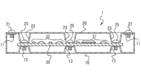
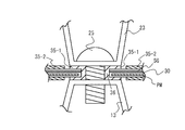
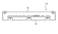
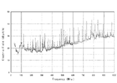
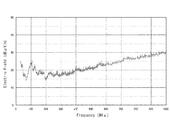
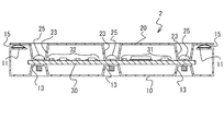
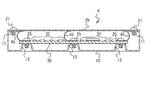
【解決手段】 電子部品31、32が実装されている配線基板30を収納する筐体1のシールド構造である。筐体1内に該筐体の内面と前記配線基板30の表面及び裏面とを接続する接続部13,23を複数備え、該接続部13,23により前記配線基板30を挟んでいる。本シールド構造によると、電子部品から発生したノイズ電流は接続部23を設けたことにより小さなループで配線基板30へ帰還させることができる。このようにノイズ電流のループ面積を小さく抑えることができる構造では、筐体1がアンテナとして作用してノイズを放射する状態を確実に防止できる。
【選択図】 図1
Description
10 本体
13 接続部
20 蓋部
21 ネジ
23 接続部
25 ネジ
30 配線基板
31、32 電子部品
Claims (9)
- 電子部品が実装されている配線基板を収納する筐体のシールド構造であって、
前記筐体と前記配線基板の表面及び裏面とを接続する接続部を複数備え、該接続部により前記配線基板を挟んでいることを特徴とする筐体のシールド構造。 - 前記接続部が、前記配線基板上に配置されているノイズ源を囲むように複数配設されていることを特徴とする請求項1に記載の筐体のシールド構造。
- 前記接続部が、前記配線基板の周部に複数配設されていることを特徴とする請求項1に記載の筐体のシールド構造。
- 前記接続部が、前記配線基板上に配置されているノイズ源を囲むと共に、該配線基板の周部に複数配設されていることを特徴とする請求項1に記載の筐体のシールド構造。
- 前記配線基板の表面に接する接続部と前記配線基板の裏面に接する接続部とが、前記配線基板を間にして上下で対向するように配置され、前記配線基板を介して導通していることを特徴とする請求項1に記載の筐体のシールド構造。
- 前記筐体が前記配線基板を支持する本体及び、該本体の上部を覆い所定の空間を形成する蓋部とを含み、前記本体及び前記蓋部のそれぞれに前記接続部が複数形成されていることを特徴とする請求項1に記載の筐体のシールド構造。
- 前記接続部が、筐体用の導電性基材を絞り加工又は曲げ加工することにより前記筐体と一体に形成されていることを特徴とする請求項1に記載の筐体のシールド構造。
- 前記接続部が、前記筐体と前記配線基板との間に配置した金属サポート又は導電性を備えた弾性体であることを特徴とする請求項1に記載の筐体のシールド構造。
- 電子部品が実装されている配線基板が、請求項1乃至8のいずれかに記載の筐体のシールド構造でシールドされていることを特徴とするシールド装置。
Priority Applications (1)
| Application Number | Priority Date | Filing Date | Title |
|---|---|---|---|
| JP2004109047A JP2005294627A (ja) | 2004-04-01 | 2004-04-01 | 筐体のシールド構造 |
Applications Claiming Priority (1)
| Application Number | Priority Date | Filing Date | Title |
|---|---|---|---|
| JP2004109047A JP2005294627A (ja) | 2004-04-01 | 2004-04-01 | 筐体のシールド構造 |
Publications (1)
| Publication Number | Publication Date |
|---|---|
| JP2005294627A true JP2005294627A (ja) | 2005-10-20 |
Family
ID=35327205
Family Applications (1)
| Application Number | Title | Priority Date | Filing Date |
|---|---|---|---|
| JP2004109047A Pending JP2005294627A (ja) | 2004-04-01 | 2004-04-01 | 筐体のシールド構造 |
Country Status (1)
| Country | Link |
|---|---|
| JP (1) | JP2005294627A (ja) |
Cited By (8)
| Publication number | Priority date | Publication date | Assignee | Title |
|---|---|---|---|---|
| CN103857267A (zh) * | 2012-11-30 | 2014-06-11 | 京瓷办公信息系统株式会社 | 电子设备的屏蔽结构 |
| JP2016102885A (ja) * | 2014-11-28 | 2016-06-02 | 京セラドキュメントソリューションズ株式会社 | 画像形成装置 |
| WO2017159531A1 (ja) * | 2016-03-16 | 2017-09-21 | 株式会社ソニー・インタラクティブエンタテインメント | 電子機器 |
| US10719756B2 (en) | 2016-11-15 | 2020-07-21 | Murata Manufacturing Co., Ltd. | UHF band RFID tag and UHF band RFID tagged article |
| JP2022133819A (ja) * | 2021-03-02 | 2022-09-14 | マツダ株式会社 | 制御ユニット構造 |
| US11457548B2 (en) | 2018-09-25 | 2022-09-27 | Hitachi Astemo, Ltd. | Electronic control device |
| DE112021008398T5 (de) | 2021-10-26 | 2024-08-01 | Hitachi Astemo, Ltd. | Elektronische steuerungseinrichtung |
| US12171071B2 (en) | 2019-11-29 | 2024-12-17 | Hitachi Astemo, Ltd. | Electronic control device |
Citations (2)
| Publication number | Priority date | Publication date | Assignee | Title |
|---|---|---|---|---|
| JP2000252676A (ja) * | 1999-02-26 | 2000-09-14 | Nec Saitama Ltd | シールドケース |
| JP2003188571A (ja) * | 2001-12-18 | 2003-07-04 | Nef:Kk | プリント基板シールド装置 |
-
2004
- 2004-04-01 JP JP2004109047A patent/JP2005294627A/ja active Pending
Patent Citations (2)
| Publication number | Priority date | Publication date | Assignee | Title |
|---|---|---|---|---|
| JP2000252676A (ja) * | 1999-02-26 | 2000-09-14 | Nec Saitama Ltd | シールドケース |
| JP2003188571A (ja) * | 2001-12-18 | 2003-07-04 | Nef:Kk | プリント基板シールド装置 |
Cited By (13)
| Publication number | Priority date | Publication date | Assignee | Title |
|---|---|---|---|---|
| US9101045B2 (en) | 2012-11-30 | 2015-08-04 | Kyocera Document Solutions Inc. | Shield structure for electronic apparatus |
| CN103857267B (zh) * | 2012-11-30 | 2017-01-11 | 京瓷办公信息系统株式会社 | 电子设备的屏蔽结构 |
| CN103857267A (zh) * | 2012-11-30 | 2014-06-11 | 京瓷办公信息系统株式会社 | 电子设备的屏蔽结构 |
| JP2016102885A (ja) * | 2014-11-28 | 2016-06-02 | 京セラドキュメントソリューションズ株式会社 | 画像形成装置 |
| US10966356B2 (en) | 2016-03-16 | 2021-03-30 | Sony Interactive Entertainment Inc. | Electronic apparatus |
| WO2017159531A1 (ja) * | 2016-03-16 | 2017-09-21 | 株式会社ソニー・インタラクティブエンタテインメント | 電子機器 |
| CN108781526A (zh) * | 2016-03-16 | 2018-11-09 | 索尼互动娱乐股份有限公司 | 电子设备 |
| US10719756B2 (en) | 2016-11-15 | 2020-07-21 | Murata Manufacturing Co., Ltd. | UHF band RFID tag and UHF band RFID tagged article |
| US11457548B2 (en) | 2018-09-25 | 2022-09-27 | Hitachi Astemo, Ltd. | Electronic control device |
| US12171071B2 (en) | 2019-11-29 | 2024-12-17 | Hitachi Astemo, Ltd. | Electronic control device |
| JP2022133819A (ja) * | 2021-03-02 | 2022-09-14 | マツダ株式会社 | 制御ユニット構造 |
| JP7567557B2 (ja) | 2021-03-02 | 2024-10-16 | マツダ株式会社 | 制御ユニット構造 |
| DE112021008398T5 (de) | 2021-10-26 | 2024-08-01 | Hitachi Astemo, Ltd. | Elektronische steuerungseinrichtung |
Similar Documents
| Publication | Publication Date | Title |
|---|---|---|
| US20090268420A1 (en) | Shielding assembly | |
| JP2017158223A (ja) | 電動モータ制御装置 | |
| JP2009158838A (ja) | 電子機器 | |
| JP2005294627A (ja) | 筐体のシールド構造 | |
| JP2008176567A (ja) | プリント基板組立体、情報技術装置用筐体及び情報技術装置 | |
| JP2009272499A (ja) | 電子制御ユニット | |
| JP2009141057A (ja) | 電子機器及びスロット | |
| US20130044419A1 (en) | Electronic device | |
| JPH0786786A (ja) | Lsiケースのシールド構造 | |
| JP5949374B2 (ja) | 電子機器 | |
| JP5294353B2 (ja) | 電磁波シールド構造 | |
| JP5022800B2 (ja) | 電子機器 | |
| TW200922439A (en) | Electronic circuit mould | |
| JP2010080691A (ja) | シールド構造及び電子機器 | |
| JP3094771B2 (ja) | 電子・通信装置ユニット構造 | |
| JP2013254925A (ja) | 電子回路装置 | |
| EP2239779B1 (en) | Flexible image-sensing module with anti-EMI function | |
| JP5257326B2 (ja) | 携帯端末機 | |
| JP2010267928A (ja) | 電子装置 | |
| JP2001007589A (ja) | プリント基板電源装置用シールド構造 | |
| JPWO2009063734A1 (ja) | 電子部品搭載機器 | |
| CN107528118A (zh) | 通信装置及其天线组件 | |
| JP2007123722A (ja) | シールド構造 | |
| JP4205720B2 (ja) | カード装置 | |
| JP2014056760A (ja) | 電子機器 |
Legal Events
| Date | Code | Title | Description |
|---|---|---|---|
| A621 | Written request for application examination |
Free format text: JAPANESE INTERMEDIATE CODE: A621 Effective date: 20070322 |
|
| A977 | Report on retrieval |
Free format text: JAPANESE INTERMEDIATE CODE: A971007 Effective date: 20090528 |
|
| A131 | Notification of reasons for refusal |
Free format text: JAPANESE INTERMEDIATE CODE: A131 Effective date: 20090609 |
|
| A521 | Written amendment |
Effective date: 20090807 Free format text: JAPANESE INTERMEDIATE CODE: A523 |
|
| A131 | Notification of reasons for refusal |
Effective date: 20090915 Free format text: JAPANESE INTERMEDIATE CODE: A131 |
|
| RD13 | Notification of appointment of power of sub attorney |
Free format text: JAPANESE INTERMEDIATE CODE: A7433 Effective date: 20091110 |
|
| A521 | Written amendment |
Effective date: 20091116 Free format text: JAPANESE INTERMEDIATE CODE: A523 |
|
| A02 | Decision of refusal |
Free format text: JAPANESE INTERMEDIATE CODE: A02 Effective date: 20091222 |
|
| A521 | Written amendment |
Free format text: JAPANESE INTERMEDIATE CODE: A523 Effective date: 20100319 |
|
| A911 | Transfer of reconsideration by examiner before appeal (zenchi) |
Free format text: JAPANESE INTERMEDIATE CODE: A911 Effective date: 20100416 |
|
| A912 | Removal of reconsideration by examiner before appeal (zenchi) |
Effective date: 20100514 Free format text: JAPANESE INTERMEDIATE CODE: A912 |