EP2239779B1 - Flexible image-sensing module with anti-EMI function - Google Patents
Flexible image-sensing module with anti-EMI function Download PDFInfo
- Publication number
- EP2239779B1 EP2239779B1 EP09162940.2A EP09162940A EP2239779B1 EP 2239779 B1 EP2239779 B1 EP 2239779B1 EP 09162940 A EP09162940 A EP 09162940A EP 2239779 B1 EP2239779 B1 EP 2239779B1
- Authority
- EP
- European Patent Office
- Prior art keywords
- unit
- conductive
- emi
- layer
- disposed
- Prior art date
- Legal status (The legal status is an assumption and is not a legal conclusion. Google has not performed a legal analysis and makes no representation as to the accuracy of the status listed.)
- Active
Links
- 239000010410 layer Substances 0.000 claims description 66
- 239000000758 substrate Substances 0.000 claims description 44
- 239000012790 adhesive layer Substances 0.000 claims description 20
- RYGMFSIKBFXOCR-UHFFFAOYSA-N Copper Chemical compound [Cu] RYGMFSIKBFXOCR-UHFFFAOYSA-N 0.000 claims description 13
- 239000011889 copper foil Substances 0.000 claims description 12
- 230000000694 effects Effects 0.000 description 4
- 239000002313 adhesive film Substances 0.000 description 3
- 238000000034 method Methods 0.000 description 3
- 239000000853 adhesive Substances 0.000 description 2
- 230000001070 adhesive effect Effects 0.000 description 2
- 239000003292 glue Substances 0.000 description 2
- 230000000295 complement effect Effects 0.000 description 1
- 230000007547 defect Effects 0.000 description 1
- 230000001419 dependent effect Effects 0.000 description 1
- 239000000463 material Substances 0.000 description 1
- 238000012986 modification Methods 0.000 description 1
- 230000004048 modification Effects 0.000 description 1
- 239000004065 semiconductor Substances 0.000 description 1
- 238000011144 upstream manufacturing Methods 0.000 description 1
Images


Classifications
-
- H—ELECTRICITY
- H01—ELECTRIC ELEMENTS
- H01L—SEMICONDUCTOR DEVICES NOT COVERED BY CLASS H10
- H01L27/00—Devices consisting of a plurality of semiconductor or other solid-state components formed in or on a common substrate
- H01L27/14—Devices consisting of a plurality of semiconductor or other solid-state components formed in or on a common substrate including semiconductor components sensitive to infrared radiation, light, electromagnetic radiation of shorter wavelength or corpuscular radiation and specially adapted either for the conversion of the energy of such radiation into electrical energy or for the control of electrical energy by such radiation
- H01L27/144—Devices controlled by radiation
- H01L27/146—Imager structures
- H01L27/14601—Structural or functional details thereof
- H01L27/14618—Containers
-
- H—ELECTRICITY
- H05—ELECTRIC TECHNIQUES NOT OTHERWISE PROVIDED FOR
- H05K—PRINTED CIRCUITS; CASINGS OR CONSTRUCTIONAL DETAILS OF ELECTRIC APPARATUS; MANUFACTURE OF ASSEMBLAGES OF ELECTRICAL COMPONENTS
- H05K1/00—Printed circuits
- H05K1/02—Details
- H05K1/0213—Electrical arrangements not otherwise provided for
- H05K1/0216—Reduction of cross-talk, noise or electromagnetic interference
- H05K1/0218—Reduction of cross-talk, noise or electromagnetic interference by printed shielding conductors, ground planes or power plane
-
- H—ELECTRICITY
- H01—ELECTRIC ELEMENTS
- H01L—SEMICONDUCTOR DEVICES NOT COVERED BY CLASS H10
- H01L2924/00—Indexing scheme for arrangements or methods for connecting or disconnecting semiconductor or solid-state bodies as covered by H01L24/00
- H01L2924/0001—Technical content checked by a classifier
- H01L2924/0002—Not covered by any one of groups H01L24/00, H01L24/00 and H01L2224/00
-
- H—ELECTRICITY
- H04—ELECTRIC COMMUNICATION TECHNIQUE
- H04N—PICTORIAL COMMUNICATION, e.g. TELEVISION
- H04N23/00—Cameras or camera modules comprising electronic image sensors; Control thereof
- H04N23/57—Mechanical or electrical details of cameras or camera modules specially adapted for being embedded in other devices
-
- H—ELECTRICITY
- H05—ELECTRIC TECHNIQUES NOT OTHERWISE PROVIDED FOR
- H05K—PRINTED CIRCUITS; CASINGS OR CONSTRUCTIONAL DETAILS OF ELECTRIC APPARATUS; MANUFACTURE OF ASSEMBLAGES OF ELECTRICAL COMPONENTS
- H05K1/00—Printed circuits
- H05K1/02—Details
- H05K1/03—Use of materials for the substrate
- H05K1/0393—Flexible materials
-
- H—ELECTRICITY
- H05—ELECTRIC TECHNIQUES NOT OTHERWISE PROVIDED FOR
- H05K—PRINTED CIRCUITS; CASINGS OR CONSTRUCTIONAL DETAILS OF ELECTRIC APPARATUS; MANUFACTURE OF ASSEMBLAGES OF ELECTRICAL COMPONENTS
- H05K1/00—Printed circuits
- H05K1/18—Printed circuits structurally associated with non-printed electric components
- H05K1/189—Printed circuits structurally associated with non-printed electric components characterised by the use of a flexible or folded printed circuit
-
- H—ELECTRICITY
- H05—ELECTRIC TECHNIQUES NOT OTHERWISE PROVIDED FOR
- H05K—PRINTED CIRCUITS; CASINGS OR CONSTRUCTIONAL DETAILS OF ELECTRIC APPARATUS; MANUFACTURE OF ASSEMBLAGES OF ELECTRICAL COMPONENTS
- H05K2201/00—Indexing scheme relating to printed circuits covered by H05K1/00
- H05K2201/07—Electric details
- H05K2201/0707—Shielding
- H05K2201/0715—Shielding provided by an outer layer of PCB
-
- H—ELECTRICITY
- H05—ELECTRIC TECHNIQUES NOT OTHERWISE PROVIDED FOR
- H05K—PRINTED CIRCUITS; CASINGS OR CONSTRUCTIONAL DETAILS OF ELECTRIC APPARATUS; MANUFACTURE OF ASSEMBLAGES OF ELECTRICAL COMPONENTS
- H05K3/00—Apparatus or processes for manufacturing printed circuits
- H05K3/0058—Laminating printed circuit boards onto other substrates, e.g. metallic substrates
-
- H—ELECTRICITY
- H05—ELECTRIC TECHNIQUES NOT OTHERWISE PROVIDED FOR
- H05K—PRINTED CIRCUITS; CASINGS OR CONSTRUCTIONAL DETAILS OF ELECTRIC APPARATUS; MANUFACTURE OF ASSEMBLAGES OF ELECTRICAL COMPONENTS
- H05K3/00—Apparatus or processes for manufacturing printed circuits
- H05K3/38—Improvement of the adhesion between the insulating substrate and the metal
- H05K3/386—Improvement of the adhesion between the insulating substrate and the metal by the use of an organic polymeric bonding layer, e.g. adhesive
Definitions
- the present invention relates to a flexible image-sensing module in particular, to a flexible image-sensing module with anti-EMI function.
- CMOS Complementary Metal-Oxide-Semiconductor
- the prior art provides an image-sensing module Da, including: a hard substrate 1a, an image sensor 2a, a plurality of electronic elements 3a, an anti-EMI (Electromagnetic Interference) element 4a, and a USB connector 5a.
- the image sensor 2a and the electronic elements 3a are electrically disposed on the hard substrate 1a.
- the image sensor 2a is exposed by the first opening 40a of the anti-EMI element 4a, and the hard substrate 1a and the electronic elements 3a are encircled by the anti-EMI element 4a.
- the thickness h1 of the hard substrate 1a and the thickness h2 of the anti-EMI element 4a cannot be reduced, so the overall thickness of the image-sensing module Da of the prior art cannot be reduced.
- the electronic elements 3a at least include: an LDO (Low Dropout) regulator 30a and a backend IC 31 a.
- the LDO regulator 30a is disposed between the USB connector 5a and the image sensor 2a and is electrically connected to the USB connector 5a.
- the backend IC 31a is far away from the LDO regulator 30a and is electrically connected to one side of the image sensor 2a.
- the image-sensing module Da is usually applied to a notebook Na.
- the image-sensing module Da is installed in a front side of a top cover Ca of the notebook Na for user to use it.
- the thickness of the image-sensing module Da of the prior art can not be reduced, so that the front side of the top cover Ca can be designed as an arc shape only.
- the whole feeling thickness of the notebook Na can not be reduced due to the arc shape formed on the front side of the top cover Ca.
- the image-sensing module Da of the prior art has the following defects:
- CMOS image-sensing chip package module of reduced thickness in order to integrate it into a portable electronic device (such as notebook) of small thickness according to different market requirements.
- the Japanese patent application no. JP 2005-303067 A discloses a shield structure of an electronic component, the shield structure comprising a first flexible layer on which an electronic component is mounted, and a multilayer circuit board having a second flexible layer a part of which is laminated and bonded on the flexible layer.
- a shield means is formed on the surface of the second flexible layer, the second flexible layer is turned up by using the laminated bonding portion as a base point, and a predetermined portion containing the electronic component is covered which becomes the shield object of the first flexible layer.
- the first flexible layer and the second flexible layer are electrically connected.
- an image digitising device comprising a housing, a circuit arranged on a first board, and an image sensor which is arranged on a second board, upstream of the opening of the housing. At least one shielding layer is arranged on the second board carrying the image sensor in order to improve the shielding effect.
- US patent application publication US 2007/0119620A1 discloses a method for shielding at least one electrical component on a flexible shielding circuit, the electrical component produces electromagnetic interference or radio frequency interference, the flexible shielding circuit including one or more signal layers and at least a first portion and a second portion and both the first portion and the second portion include one or more of the signal layers, the method comprising: mounting the electrical component on the first portion of the flexible shielding circuit; covering at least one exposed surface of the electrical component that is mounted on the first portion with the second portion of the flexible shielding circuit; and selectively securing the second portion of the flexible shielding circuit to the first portion, wherein the second portion provides shielding for the electrical component.
- the present invention provides a flexible image-sensing module with anti-EMI function having the technical features according to claim 1.
- Preferred embodiments of the present invention are stated in the dependent claims.
- Advantages of the present invention are that the whole thickness of the flexible image-sensing module can be reduced, and the flexible image-sensing module is not easily cracked when assembling the flexible image-sensing module.
- an illustrative example provides a flexible thin image-sensing module with anti-EMI function, including: a flexible substrate unit, a first conductive unit, a protection unit, an anti-EMI unit, a second conductive layer, an electronic element unit, and a third conductive unit.
- the flexible substrate unit has at least one through hole.
- the first conductive unit has a first conductive layer disposed on a bottom surface of the flexible substrate unit, a second conductive layer disposed on a top surface of the flexible substrate unit, and a third conductive layer disposed on an inner surface of the through hole and electrically connected between the first conductive layer and the second conductive layer.
- the protection unit has a first adhesive layer disposed on the first conductive layer, a first covering layer disposed on the first adhesive layer, a second adhesive layer disposed on the second conductive layer, and a second covering layer disposed on the second adhesive layer.
- the protection unit has at least one first hole passing through the first adhesive layer and the first covering layer and a plurality of second holes passing through the second adhesive layer and the second covering layer.
- the anti-EMI unit is disposed on the first covering layer.
- the second conductive unit has a first conductive body filling out the first hole, and the first conductive body is electrically connected between the first conductive layer and the anti-EMI unit.
- the electronic element unit has a plurality of electronic elements disposed on the second covering layer, and one of the electronic elements is an image sensor.
- the third conductive unit has a plurality of second conductive bodies respectively filling out the second holes, and the second conductive bodies are electrically connected between the second conductive layer and the electronic element unit.
- an illustrative example provides a flexible thin image-sensing module with anti-EMI function, including: a flexible substrate unit, an electronic element unit, an anti-EMI unit, and a conductive structure.
- the electronic element unit has a plurality of electronic elements disposed on a top surface of the flexible substrate unit, and the electronic elements at least include an image sensor, a low dropout regulator and a backend IC.
- the anti-EMI unit is disposed on a bottom surface of the flexible substrate unit.
- the conductive structure passes through the flexible substrate unit and is electrically connected between the electronic element unit and the anti-EMI unit in order to guide electromagnetic waves generated by the electronic element unit to the anti-EMI unit.
- the present invention provides a flexible thin image-sensing module D with anti-EMI (Anti Electromagnetic Interference) function, including: a flexible substrate unit 1, a first conductive unit 2, a protection unit 3, an anti-EMI unit 4, a second conductive layer 5, an electronic element unit 6, and a third conductive unit 7.
- EMI Anti Electromagnetic Interference
- the flexible substrate unit 1 has at least one through hole 100.
- the flexible substrate unit 1 can be a flexible copper foil clad laminate (FCCL).
- FCCL flexible copper foil clad laminate
- the flexible substrate unit 1 has a base film 11, a first base copper foil 12 disposed on a top surface of the base film 11 and a second base copper foil 13 disposed on a bottom surface of the base film 11, and the through hole 100 passes through the first base copper foil 12, the base film 11 and the second base copper foil 13.
- FCCL is just an example, and it does not limit the present invention. Any elastic substrate or flexible substrate can be applied in the present invention.
- the first conductive unit 2 has a first conductive layer 21 disposed on a bottom surface of the flexible substrate unit 1, a second conductive layer 22 disposed on a top surface of the flexible substrate unit 1, and a third conductive layer 23 disposed on an inner surface of the through hole 100 and electrically connected between the first conductive layer 21 and the second conductive layer 22.
- the first conductive unit 2 can be an electrodeposited copper foil.
- the third conductive layer 23 also can completely fill out the through hole 100 according to different requirements.
- the protection unit 3 has a first adhesive layer 31 disposed on the first conductive layer 21, a first covering layer 32 disposed on the first adhesive layer 31, a second adhesive layer 33 disposed on the second conductive layer 22, and a second covering layer 34 disposed on the second adhesive layer 33.
- the protection unit 3 has at least one first hole 301 passing through the first adhesive layer 31 and the first covering layer 32 and a plurality of second holes 302 passing through the second adhesive layer 33 and the second covering layer 34.
- the anti-EMI unit 4 is disposed on the first covering layer 32, and the anti-EMI unit 4 can be a grounding film for guiding electromagnetic waves generated by the electronic element unit 6 to the anti-EMI unit 4 in order to decrease the electromagnetic interference of the electronic element unit 6.
- the total thickness of the flexible substrate unit 1, the first conductive unit 2 and the anti-EMI unit 4 is between 0.1mm and 0.35mm. For example, 0.1mm ⁇ the total thickness ⁇ 0.35mm.
- the second conductive unit 5 has a first conductive body 50 filling out the first hole 301, and the first conductive body 50 is electrically connected between the first conductive layer 21 of the first conductive unit 2 and the anti-EMI unit 4.
- the electronic element unit 6 has a plurality of electronic elements 60 disposed on the second covering layer 34, and the electronic elements at least comprise an image sensor, a low dropout (LDO) regulator and a backend IC.
- the above-mentioned electronic elements are just examples, and these do not limit the present invention.
- the third conductive unit 7 has a plurality of second conductive bodies 70 respectively filling out the second holes 302, and the second conductive bodies 70 are electrically connected between the second conductive layer 22 of the first conductive unit 2 and the electronic element unit 6.
- the present invention further includes an adhesive unit 8 that has a plurality of adhesive films 80 disposed on the anti-EMI unit 4.
- Each adhesive film 80 can be a film with adhesive function and without conductive function.
- the flexible thin image-sensing module D can be positioned on any object via the adhesive films 80.
- the present invention provides a flexible thin image-sensing module D with anti-EMI function, including: a flexible substrate unit 1, an electronic element unit 6, an anti-EMI unit 4 and a conductive structure.
- the electronic element unit 6 has a plurality of electronic elements 60 disposed on a top surface of the flexible substrate unit 1, and the electronic elements 60 at least includes an image sensor, a low dropout regulator and a backend IC.
- the anti-EMI unit 4 is disposed on a bottom surface of the flexible substrate unit 1.
- the conductive structure is composed of a first conductive unit 2, a protection unit 3, a second conductive unit 5 and a third conductive unit 7, and the conductive structure passes through the flexible substrate unit 1 and is electrically connected between the electronic element unit 6 and the anti-EMI unit 4 in order to guide electromagnetic waves generated by the electronic element unit 6 to the anti-EMI unit 4.
- the present invention provides a flexible thin PCB module with anti-EMI function.
- the flexible thin PCB module can be applied to different fields according to the types of the electronic elements 60.
- the flexible thin PCB module includes a flexible substrate unit 1, an electronic element unit 6, an anti-EMI unit 4 and a conductive structure.
- the electronic element unit 6 has a plurality of electronic elements 60 disposed on a top surface of the flexible substrate unit 1.
- the anti-EMI unit 4 is disposed on a bottom surface of the flexible substrate unit 1.
- the conductive structure is composed of a first conductive unit 2, a protection unit 3, a second conductive unit 5 and a third conductive unit 7, and the conductive structure passes through the flexible substrate unit 1 and is electrically connected between the electronic element unit 6 and the anti-EMI unit 4 in order to guide electromagnetic waves generated by the electronic element unit 6 to the anti-EMI unit 4.
- the front side of the top cover C can be designed as an inclination shape due to the reduced thickness of the flexible thin image-sensing module D.
- the whole feeling thickness of the notebook N is reduced due to the inclination shape formed on the front side of the top cover C.
- the present invention has the following advantages:
Description
- The present invention relates to a flexible image-sensing module in particular, to a flexible image-sensing module with anti-EMI function.
- The advantage of CMOS (Complementary Metal-Oxide-Semiconductor) is low power consumption and small size, so that the CMOS image-sensing chip package module can integrate into small portable electronic devices such as mobile phone and notebook.
- Referring to
FIGS. 1A to 1D , the prior art provides an image-sensing module Da, including: a hard substrate 1a, animage sensor 2a, a plurality ofelectronic elements 3a, an anti-EMI (Electromagnetic Interference)element 4a, and aUSB connector 5a. Theimage sensor 2a and theelectronic elements 3a are electrically disposed on the hard substrate 1a. Theimage sensor 2a is exposed by thefirst opening 40a of theanti-EMI element 4a, and the hard substrate 1a and theelectronic elements 3a are encircled by theanti-EMI element 4a. Hence, the thickness h1 of the hard substrate 1a and the thickness h2 of theanti-EMI element 4a cannot be reduced, so the overall thickness of the image-sensing module Da of the prior art cannot be reduced. - Moreover, the
electronic elements 3a at least include: an LDO (Low Dropout)regulator 30a and abackend IC 31 a. The LDOregulator 30a is disposed between theUSB connector 5a and theimage sensor 2a and is electrically connected to theUSB connector 5a. Thebackend IC 31a is far away from the LDOregulator 30a and is electrically connected to one side of theimage sensor 2a. - Referring to
FIG. 1D , the image-sensing module Da is usually applied to a notebook Na. For example, the image-sensing module Da is installed in a front side of a top cover Ca of the notebook Na for user to use it. However, the thickness of the image-sensing module Da of the prior art can not be reduced, so that the front side of the top cover Ca can be designed as an arc shape only. Hence, the whole feeling thickness of the notebook Na can not be reduced due to the arc shape formed on the front side of the top cover Ca. - Hence, the image-sensing module Da of the prior art has the following defects:
- 1. Because the thickness of the hard substrate 1 a is large, the thickness of the image-sensing module Da cannot be reduced.
- 2. The image-sensing module Da needs to use the
anti-EMI element 4a to prevent theelectronic elements 3a from being affected by electromagnetic interference, so that the thickness of the image-sensing module Da cannot be reduced. - 3. The hard substrate 1a is made of hard material, so that the hard substrate 1a is cracked easily when assembling the image-sensing module Da. In addition, the prior art has provided a way to prevent the hard substrate 1a from being cracked easily, and the way is to increase the thickness of the hard substrate 1a. However, this way would increase the cost and increase the whole thickness of the image-sensing module Da.
- 4. If the
anti-EMI element 4a wants to achieve anti-EMI effect, theanti-EMI element 4a needs to mate with conductive glue. - Hence, it is very important for designer to design a CMOS image-sensing chip package module of reduced thickness in order to integrate it into a portable electronic device (such as notebook) of small thickness according to different market requirements.
- The Japanese patent application no.
JP 2005-303067 A - In the International patent application no.
WO 2006/072518 A1 there is disclosed an image digitising device comprising a housing, a circuit arranged on a first board, and an image sensor which is arranged on a second board, upstream of the opening of the housing. At least one shielding layer is arranged on the second board carrying the image sensor in order to improve the shielding effect. Further, US patent application publicationUS 2007/0119620A1 discloses a method for shielding at least one electrical component on a flexible shielding circuit, the electrical component produces electromagnetic interference or radio frequency interference, the flexible shielding circuit including one or more signal layers and at least a first portion and a second portion and both the first portion and the second portion include one or more of the signal layers, the method comprising: mounting the electrical component on the first portion of the flexible shielding circuit; covering at least one exposed surface of the electrical component that is mounted on the first portion with the second portion of the flexible shielding circuit; and selectively securing the second portion of the flexible shielding circuit to the first portion, wherein the second portion provides shielding for the electrical component. - In view of the aforementioned issues, the present invention provides a flexible image-sensing module with anti-EMI function having the technical features according to
claim 1. Preferred embodiments of the present invention are stated in the dependent claims. - Advantages of the present invention are that the whole thickness of the flexible image-sensing module can be reduced, and the flexible image-sensing module is not easily cracked when assembling the flexible image-sensing module.
- To achieve the above-mentioned objectives, an illustrative example provides a flexible thin image-sensing module with anti-EMI function, including: a flexible substrate unit, a first conductive unit, a protection unit, an anti-EMI unit, a second conductive layer, an electronic element unit, and a third conductive unit. The flexible substrate unit has at least one through hole. The first conductive unit has a first conductive layer disposed on a bottom surface of the flexible substrate unit, a second conductive layer disposed on a top surface of the flexible substrate unit, and a third conductive layer disposed on an inner surface of the through hole and electrically connected between the first conductive layer and the second conductive layer. The protection unit has a first adhesive layer disposed on the first conductive layer, a first covering layer disposed on the first adhesive layer, a second adhesive layer disposed on the second conductive layer, and a second covering layer disposed on the second adhesive layer. The protection unit has at least one first hole passing through the first adhesive layer and the first covering layer and a plurality of second holes passing through the second adhesive layer and the second covering layer. The anti-EMI unit is disposed on the first covering layer. The second conductive unit has a first conductive body filling out the first hole, and the first conductive body is electrically connected between the first conductive layer and the anti-EMI unit. The electronic element unit has a plurality of electronic elements disposed on the second covering layer, and one of the electronic elements is an image sensor. The third conductive unit has a plurality of second conductive bodies respectively filling out the second holes, and the second conductive bodies are electrically connected between the second conductive layer and the electronic element unit.
- To achieve the above-mentioned objectives, an illustrative example provides a flexible thin image-sensing module with anti-EMI function, including: a flexible substrate unit, an electronic element unit, an anti-EMI unit, and a conductive structure. The electronic element unit has a plurality of electronic elements disposed on a top surface of the flexible substrate unit, and the electronic elements at least include an image sensor, a low dropout regulator and a backend IC. The anti-EMI unit is disposed on a bottom surface of the flexible substrate unit. The conductive structure passes through the flexible substrate unit and is electrically connected between the electronic element unit and the anti-EMI unit in order to guide electromagnetic waves generated by the electronic element unit to the anti-EMI unit.
- In order to further understand the techniques, means and effects the present invention takes for achieving the prescribed objectives, the following detailed descriptions and appended drawings are hereby referred, such that, through which, the purposes, features and aspects of the present invention can be thoroughly and concretely appreciated; however, the appended drawings are merely provided for reference and illustration, without any intention to be used for limiting the present invention.
-
-
FIG. 1A is a top, schematic view of the image-sensing module of the prior art; -
FIG. 1B is a front, schematic view of the image-sensing module of the prior art; -
FIG. 1C is a cross-sectional, schematic view alongline 1C-1C of the image-sensing module shown inFig. 1B ; -
FIG. 1D is lateral, schematic view of the image-sensing module of the prior art applied to the notebook; -
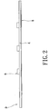
FIG. 2 is a lateral, schematic view of the flexible thin image-sensing module with anti-EMI function according to the present invention; -
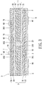
FIG. 3 is a lateral, cross-sectional, schematic view of the flexible thin image-sensing module with anti-EMI function according to the present invention; and -
FIG. 4 is a lateral, schematic view of the flexible thin image-sensing module with anti-EMI function applied to the notebook according to the present invention. - Referring to
FIGS. 2 and3 , the present invention provides a flexible thin image-sensing module D with anti-EMI (Anti Electromagnetic Interference) function, including: aflexible substrate unit 1, a firstconductive unit 2, aprotection unit 3, ananti-EMI unit 4, a secondconductive layer 5, anelectronic element unit 6, and a thirdconductive unit 7. - The
flexible substrate unit 1 has at least one throughhole 100. In the present invention, theflexible substrate unit 1 can be a flexible copper foil clad laminate (FCCL). For example, theflexible substrate unit 1 has abase film 11, a firstbase copper foil 12 disposed on a top surface of thebase film 11 and a second base copper foil 13 disposed on a bottom surface of thebase film 11, and the throughhole 100 passes through the firstbase copper foil 12, thebase film 11 and the second base copper foil 13. However, the FCCL is just an example, and it does not limit the present invention. Any elastic substrate or flexible substrate can be applied in the present invention. - Moreover, the first
conductive unit 2 has a first conductive layer 21 disposed on a bottom surface of theflexible substrate unit 1, a second conductive layer 22 disposed on a top surface of theflexible substrate unit 1, and a thirdconductive layer 23 disposed on an inner surface of the throughhole 100 and electrically connected between the first conductive layer 21 and the second conductive layer 22. In the present embodiment, the firstconductive unit 2 can be an electrodeposited copper foil. The thirdconductive layer 23 also can completely fill out the throughhole 100 according to different requirements. - Furthermore, the
protection unit 3 has a firstadhesive layer 31 disposed on the first conductive layer 21, afirst covering layer 32 disposed on the firstadhesive layer 31, a secondadhesive layer 33 disposed on the second conductive layer 22, and asecond covering layer 34 disposed on the secondadhesive layer 33. In addition, theprotection unit 3 has at least onefirst hole 301 passing through the firstadhesive layer 31 and thefirst covering layer 32 and a plurality ofsecond holes 302 passing through the secondadhesive layer 33 and thesecond covering layer 34. - Moreover, the
anti-EMI unit 4 is disposed on thefirst covering layer 32, and theanti-EMI unit 4 can be a grounding film for guiding electromagnetic waves generated by theelectronic element unit 6 to theanti-EMI unit 4 in order to decrease the electromagnetic interference of theelectronic element unit 6. Furthermore, the total thickness of theflexible substrate unit 1, the firstconductive unit 2 and theanti-EMI unit 4 is between 0.1mm and 0.35mm. For example, 0.1mm □ the total thickness < 0.35mm. - In addition, the second
conductive unit 5 has a firstconductive body 50 filling out thefirst hole 301, and the firstconductive body 50 is electrically connected between the first conductive layer 21 of the firstconductive unit 2 and theanti-EMI unit 4. - Moreover, the
electronic element unit 6 has a plurality ofelectronic elements 60 disposed on thesecond covering layer 34, and the electronic elements at least comprise an image sensor, a low dropout (LDO) regulator and a backend IC. However, the above-mentioned electronic elements are just examples, and these do not limit the present invention. - Furthermore, the third
conductive unit 7 has a plurality of secondconductive bodies 70 respectively filling out thesecond holes 302, and the secondconductive bodies 70 are electrically connected between the second conductive layer 22 of the firstconductive unit 2 and theelectronic element unit 6. - In addition, the present invention further includes an adhesive unit 8 that has a plurality of
adhesive films 80 disposed on theanti-EMI unit 4. Eachadhesive film 80 can be a film with adhesive function and without conductive function. Hence, the flexible thin image-sensing module D can be positioned on any object via theadhesive films 80. - Therefore, the present invention provides a flexible thin image-sensing module D with anti-EMI function, including: a
flexible substrate unit 1, anelectronic element unit 6, ananti-EMI unit 4 and a conductive structure. Moreover, theelectronic element unit 6 has a plurality ofelectronic elements 60 disposed on a top surface of theflexible substrate unit 1, and theelectronic elements 60 at least includes an image sensor, a low dropout regulator and a backend IC. Theanti-EMI unit 4 is disposed on a bottom surface of theflexible substrate unit 1. The conductive structure is composed of a firstconductive unit 2, aprotection unit 3, a secondconductive unit 5 and a thirdconductive unit 7, and the conductive structure passes through theflexible substrate unit 1 and is electrically connected between theelectronic element unit 6 and theanti-EMI unit 4 in order to guide electromagnetic waves generated by theelectronic element unit 6 to theanti-EMI unit 4. - If the types of the
electronic elements 60 do not be limited, the present invention provides a flexible thin PCB module with anti-EMI function. The flexible thin PCB module can be applied to different fields according to the types of theelectronic elements 60. Moreover, the flexible thin PCB module includes aflexible substrate unit 1, anelectronic element unit 6, ananti-EMI unit 4 and a conductive structure. In addition, theelectronic element unit 6 has a plurality ofelectronic elements 60 disposed on a top surface of theflexible substrate unit 1. Theanti-EMI unit 4 is disposed on a bottom surface of theflexible substrate unit 1. The conductive structure is composed of a firstconductive unit 2, aprotection unit 3, a secondconductive unit 5 and a thirdconductive unit 7, and the conductive structure passes through theflexible substrate unit 1 and is electrically connected between theelectronic element unit 6 and theanti-EMI unit 4 in order to guide electromagnetic waves generated by theelectronic element unit 6 to theanti-EMI unit 4. - Furthermore, referring to
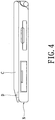
FIG. 4 , when the flexible thin image-sensing module D is installed in a front side of a top cover C of a notebook N, the front side of the top cover C can be designed as an inclination shape due to the reduced thickness of the flexible thin image-sensing module D. Hence, the whole feeling thickness of the notebook N is reduced due to the inclination shape formed on the front side of the top cover C. - In conclusion, the present invention has the following advantages:
- 1. The
anti-EMI unit 4 is disposed on the bottom surface of theflexible substrate unit 1, and theanti-EMI unit 4 can be a grounding film for guiding electromagnetic waves generated by theelectronic element unit 6 to theanti-EMI unit 4 in order to decrease the electromagnetic interference of theelectronic element unit 6. - 2. The
anti-EMI unit 4 is disposed on the bottom surface of theflexible substrate unit 1, so that the whole feeling thickness of the notebook N is reduced. - 3. The flexible thin image-sensing module D and the flexible thin PCB module are flexible, so that the flexible thin image-sensing module D and the flexible thin PCB module do not be cracked easily when assembling the flexible thin image-sensing module D and the flexible thin PCB module.
- 4. The
anti-EMI unit 4 can achieve anti-EMI effect without using conductive glue. - The above-mentioned descriptions represent merely the preferred embodiment of the present invention, without any intention to limit the scope of the present invention thereto. Various equivalent changes, alternations or modifications based on the claims of present invention are all consequently viewed as being embraced by the scope of the present invention.
Claims (3)
- A flexible image-sensing module (D) with anti-EMI function, comprising:a flexible substrate unit (1) having at least one through hole (100) passing therethrough;a first conductive unit (2) having a first conductive layer (21) disposed on a bottom surface of the flexible substrate unit (1), a second conductive layer (22) disposed on a top surface of the flexible substrate unit (1), and a third conductive layer (23) passing through the through hole (100), and electrically connected between the first conductive layer (21) and the second conductive layer (22);a protection unit (3) having a first adhesive layer (31) disposed on the first conductive layer (21), a first covering layer (32) disposed on the first adhesive layer (31), a second adhesive layer (33) disposed on the second conductive layer (22), and a second covering layer (34) disposed on the second adhesive layer (33), wherein the protection unit (3) has at least one first hole (301) passing through the first adhesive layer (31) and the first covering layer (32) and a plurality of second holes (302) passing through the second adhesive layer (33) and the second covering layer (34);an anti-EMI unit (4) disposed on the first covering layer (32);a second conductive unit (5) having a first conductive body (50), wherein the first hole (301) is filled with the first conductive body (50), and the first conductive body (50) has two ends electrically contacting the first conductive layer (21) and the anti-EMI unit (4), respectively;an electronic element unit (6) having a plurality of electronic elements (60) disposed on the second covering layer (34), wherein one of the electronic elements (60) is an image sensor, and the electronic elements (60) are exposed from the flexible image-sensing module (D); anda third conductive unit (7) having a plurality of second conductive bodies (70),wherein the second holes (302) are respectively filled with the second conductive bodies (70), and each of the second conductive bodies (70) has two ends electrically contacting the second conductive layer (22) and the corresponding electronic element (6), respectively;wherein the anti-EMI unit (4), the first covering layer (32), the first adhesive layer (31), the first conductive layer (21), the flexible substrate unit (1), the second conductive layer (22), the second adhesive layer (33), the second covering layer (34) and the electronic element unit (6) are disposed on top of one another, wherein the anti-EMI unit (4) and the electronic element unit (6) are disposed on two opposite sides of the flexible image-sensing module (D), the anti-EMI unit (4) is a bottommost unit of the flexible image-sensing module (D), and the electronic element unit (6) is a topmost unit of the flexible image-sensing module (D);wherein the electronic elements (60) are electrically connected to the anti-EMI unit (4) through the second conductive bodies (70), the second conductive layer (22), the third conductive layer (23), the first conductive layer (21) and the first conductive body (50) in sequence;wherein the total thickness of the flexible substrate unit (1), the first conductive unit (2) and the anti-EMI unit (4) is between 0.1 mm and 0.35 mm;wherein the image sensor (60) and the anti-EMI unit (4) are respectively disposed on two opposite surfaces of the protection unit (3);wherein the image sensor (60) and the anti-EMI unit (4) are exposed outside the protection unit (3) and the flexible substrate unit (1);wherein the image sensor (60) and the anti-EMI unit (4) are connected with each other through the second conductive bodies (70) inside the protection unit (3), the first conductive unit (2) inside the flexible substrate unit (1), and the first conductive body (50) inside the protection unit (3).
- The flexible image-sensing module (D) according to claim 1, wherein the flexible substrate unit (1) is a flexible copper foil clad laminate and has a base film (11), a first base copper foil (12) disposed on a top surface of the base film (11) and a second base copper foil disposed on a bottom surface of the base film (11), and the through hole (100) passes through the first base copper foil (12), the base film (11) and the second base copper foil.
- The flexible image-sensing module (D) according to claim 1, wherein the first conductive unit (2) is an electrodeposited copper foil, the electronic elements (60) at least comprise a low dropout regulator and a backend IC, and the anti-EMI unit (4) is a grounding film.
Applications Claiming Priority (1)
| Application Number | Priority Date | Filing Date | Title |
|---|---|---|---|
| TW098111647A TWI372558B (en) | 2009-04-08 | 2009-04-08 | Flexible thin image-sensing module with anti-emi function and flexible thin pcb module with anti-emi function |
Publications (3)
| Publication Number | Publication Date |
|---|---|
| EP2239779A2 EP2239779A2 (en) | 2010-10-13 |
| EP2239779A3 EP2239779A3 (en) | 2012-09-26 |
| EP2239779B1 true EP2239779B1 (en) | 2017-05-24 |
Family
ID=41127907
Family Applications (1)
| Application Number | Title | Priority Date | Filing Date |
|---|---|---|---|
| EP09162940.2A Active EP2239779B1 (en) | 2009-04-08 | 2009-06-17 | Flexible image-sensing module with anti-EMI function |
Country Status (3)
| Country | Link |
|---|---|
| US (1) | US8093509B2 (en) |
| EP (1) | EP2239779B1 (en) |
| TW (1) | TWI372558B (en) |
Families Citing this family (3)
| Publication number | Priority date | Publication date | Assignee | Title |
|---|---|---|---|---|
| US8670588B2 (en) * | 2009-09-08 | 2014-03-11 | Apple Inc. | Handheld device assembly |
| CN109949526B (en) * | 2017-12-20 | 2023-11-03 | 上海箱箱物流科技有限公司 | Logistics appliance and anti-disassembly method thereof |
| KR102058865B1 (en) * | 2018-04-12 | 2019-12-24 | (주)아이엠 | Heating device using hyper heat accelerator and method for manufacturing the same |
Citations (2)
| Publication number | Priority date | Publication date | Assignee | Title |
|---|---|---|---|---|
| US20040222352A1 (en) * | 2003-05-09 | 2004-11-11 | Matsushita Electric Industrial Co., Ltd. | Imaging apparatus |
| US20070119620A1 (en) * | 2005-11-29 | 2007-05-31 | Rodriguez Jose F | Flexible circuit shields |
Family Cites Families (13)
| Publication number | Priority date | Publication date | Assignee | Title |
|---|---|---|---|---|
| JPH07506223A (en) * | 1993-02-11 | 1995-07-06 | テレフオンアクチーボラゲツト エル エム エリクソン | Flexible device to encapsulate electronic components |
| US5519585A (en) * | 1993-04-12 | 1996-05-21 | Dell Usa, L.P. | Sandwiched insulative/conductive layer EMI shield structure for printed circuit board |
| SE504195C2 (en) * | 1995-03-21 | 1996-12-02 | Ericsson Telefon Ab L M | Laminates for sealing and enclosing electronic components, as well as methods for making them |
| US5917149A (en) * | 1997-05-15 | 1999-06-29 | Daimlerchrysler Corporation | Flexible circuit board interconnect with strain relief |
| GB2351183B (en) * | 1999-06-18 | 2003-10-15 | Nokia Mobile Phones Ltd | Shielding can for a printed circuit board |
| JP2001244583A (en) * | 2000-02-29 | 2001-09-07 | Fuji Photo Optical Co Ltd | Flexible circuit board |
| US6900383B2 (en) * | 2001-03-19 | 2005-05-31 | Hewlett-Packard Development Company, L.P. | Board-level EMI shield that adheres to and conforms with printed circuit board component and board surfaces |
| US20030214802A1 (en) * | 2001-06-15 | 2003-11-20 | Fjelstad Joseph C. | Signal transmission structure with an air dielectric |
| JP2005303067A (en) | 2004-04-13 | 2005-10-27 | Mitsubishi Electric Corp | Shield structure of electronic component |
| DE102005000655A1 (en) | 2005-01-04 | 2006-07-13 | Robert Bosch Gmbh | Image capture device |
| EP1951016B1 (en) * | 2006-10-30 | 2013-05-29 | Ibiden Co., Ltd. | Flex-rigid wiring board and method for manufacturing the same |
| US7977582B2 (en) * | 2008-01-28 | 2011-07-12 | International Business Machines Corporation | Flexible multilayer printed circuit assembly with reduced EMI emissions |
| KR101098072B1 (en) * | 2008-03-10 | 2011-12-26 | 이비덴 가부시키가이샤 | Flexible wiring board and method of manufacturing same |
-
2009
- 2009-04-08 TW TW098111647A patent/TWI372558B/en active
- 2009-06-09 US US12/457,347 patent/US8093509B2/en active Active
- 2009-06-17 EP EP09162940.2A patent/EP2239779B1/en active Active
Patent Citations (2)
| Publication number | Priority date | Publication date | Assignee | Title |
|---|---|---|---|---|
| US20040222352A1 (en) * | 2003-05-09 | 2004-11-11 | Matsushita Electric Industrial Co., Ltd. | Imaging apparatus |
| US20070119620A1 (en) * | 2005-11-29 | 2007-05-31 | Rodriguez Jose F | Flexible circuit shields |
Also Published As
| Publication number | Publication date |
|---|---|
| TWI372558B (en) | 2012-09-11 |
| EP2239779A2 (en) | 2010-10-13 |
| TW201038059A (en) | 2010-10-16 |
| US20100258343A1 (en) | 2010-10-14 |
| US8093509B2 (en) | 2012-01-10 |
| EP2239779A3 (en) | 2012-09-26 |
Similar Documents
| Publication | Publication Date | Title |
|---|---|---|
| US10860054B2 (en) | Electronic devices with cover layers mounted to displays | |
| TWI603467B (en) | Narrow border displays for electronic devices | |
| US9098242B2 (en) | Electronic devices with cover layers mounted to displays | |
| US8969730B2 (en) | Printed circuit solder connections | |
| EP3683650B1 (en) | Display screen assembly and mobile terminal | |
| US7952889B2 (en) | Stacking structure of printed circuit board | |
| US8054639B2 (en) | Image-sensing module for reducing overall thickness thereof and preventing EMI | |
| US9345134B2 (en) | Printed wiring board | |
| US20090073672A1 (en) | Electromagnetic shield and electronic device using the same | |
| US20100025085A1 (en) | Electronic apparatus, flexible printed wiring board and method for manufacturing flexible printed wiring board | |
| CN105960157A (en) | Electromagnetic shielding protection film and FPC (flexible printed circuit) | |
| EP2239779B1 (en) | Flexible image-sensing module with anti-EMI function | |
| CN107396621B (en) | Electromagnetic shield for electronic device | |
| US7813138B2 (en) | Electronic device | |
| WO2018235730A1 (en) | Display module | |
| JP2008078205A (en) | Substrate assembly and method for manufacturing the same, electronic component assembly and method for manufacturing the same, and electronic apparatus | |
| TW201408149A (en) | Circuit board assembly and camera module | |
| US20030220129A1 (en) | Mobile phone with dual PCB structure | |
| US8305765B2 (en) | Electronic apparatus | |
| CN106445218B (en) | Touch control panel and circuit board thereof | |
| WO2021185237A1 (en) | Circuit board assembly and electronic device | |
| CN112449477B (en) | Circuit board manufacturing method and circuit board | |
| CN101877347B (en) | Flexible and thin image sensing module with electromagnetic interference prevention and circuit board module | |
| KR20100082180A (en) | Electronic apparatus having electro-magnetic interference shielding | |
| US10854362B2 (en) | Guide-connected contactor and portable electronic device comprising same |
Legal Events
| Date | Code | Title | Description |
|---|---|---|---|
| PUAI | Public reference made under article 153(3) epc to a published international application that has entered the european phase |
Free format text: ORIGINAL CODE: 0009012 |
|
| AK | Designated contracting states |
Kind code of ref document: A2 Designated state(s): AT BE BG CH CY CZ DE DK EE ES FI FR GB GR HR HU IE IS IT LI LT LU LV MC MK MT NL NO PL PT RO SE SI SK TR |
|
| AX | Request for extension of the european patent |
Extension state: AL BA RS |
|
| PUAL | Search report despatched |
Free format text: ORIGINAL CODE: 0009013 |
|
| AK | Designated contracting states |
Kind code of ref document: A3 Designated state(s): AT BE BG CH CY CZ DE DK EE ES FI FR GB GR HR HU IE IS IT LI LT LU LV MC MK MT NL NO PL PT RO SE SI SK TR |
|
| AX | Request for extension of the european patent |
Extension state: AL BA RS |
|
| RIC1 | Information provided on ipc code assigned before grant |
Ipc: H01L 27/146 20060101AFI20120817BHEP |
|
| 17P | Request for examination filed |
Effective date: 20130107 |
|
| 17Q | First examination report despatched |
Effective date: 20130627 |
|
| REG | Reference to a national code |
Ref country code: DE Ref legal event code: R079 Ref document number: 602009046237 Country of ref document: DE Free format text: PREVIOUS MAIN CLASS: H01L0027146000 Ipc: H05K0001180000 |
|
| GRAP | Despatch of communication of intention to grant a patent |
Free format text: ORIGINAL CODE: EPIDOSNIGR1 |
|
| INTG | Intention to grant announced |
Effective date: 20161215 |
|
| RIC1 | Information provided on ipc code assigned before grant |
Ipc: H05K 1/18 20060101AFI20161206BHEP Ipc: H01L 27/146 20060101ALI20161206BHEP Ipc: H05K 1/02 20060101ALI20161206BHEP |
|
| GRAS | Grant fee paid |
Free format text: ORIGINAL CODE: EPIDOSNIGR3 |
|
| GRAA | (expected) grant |
Free format text: ORIGINAL CODE: 0009210 |
|
| AK | Designated contracting states |
Kind code of ref document: B1 Designated state(s): AT BE BG CH CY CZ DE DK EE ES FI FR GB GR HR HU IE IS IT LI LT LU LV MC MK MT NL NO PL PT RO SE SI SK TR |
|
| REG | Reference to a national code |
Ref country code: GB Ref legal event code: FG4D |
|
| REG | Reference to a national code |
Ref country code: CH Ref legal event code: EP |
|
| REG | Reference to a national code |
Ref country code: IE Ref legal event code: FG4D |
|
| REG | Reference to a national code |
Ref country code: AT Ref legal event code: REF Ref document number: 896590 Country of ref document: AT Kind code of ref document: T Effective date: 20170615 |
|
| REG | Reference to a national code |
Ref country code: FR Ref legal event code: PLFP Year of fee payment: 9 |
|
| REG | Reference to a national code |
Ref country code: DE Ref legal event code: R096 Ref document number: 602009046237 Country of ref document: DE |
|
| REG | Reference to a national code |
Ref country code: NL Ref legal event code: MP Effective date: 20170524 |
|
| REG | Reference to a national code |
Ref country code: LT Ref legal event code: MG4D |
|
| REG | Reference to a national code |
Ref country code: AT Ref legal event code: MK05 Ref document number: 896590 Country of ref document: AT Kind code of ref document: T Effective date: 20170524 |
|
| PG25 | Lapsed in a contracting state [announced via postgrant information from national office to epo] |
Ref country code: AT Free format text: LAPSE BECAUSE OF FAILURE TO SUBMIT A TRANSLATION OF THE DESCRIPTION OR TO PAY THE FEE WITHIN THE PRESCRIBED TIME-LIMIT Effective date: 20170524 Ref country code: NO Free format text: LAPSE BECAUSE OF FAILURE TO SUBMIT A TRANSLATION OF THE DESCRIPTION OR TO PAY THE FEE WITHIN THE PRESCRIBED TIME-LIMIT Effective date: 20170824 Ref country code: HR Free format text: LAPSE BECAUSE OF FAILURE TO SUBMIT A TRANSLATION OF THE DESCRIPTION OR TO PAY THE FEE WITHIN THE PRESCRIBED TIME-LIMIT Effective date: 20170524 Ref country code: ES Free format text: LAPSE BECAUSE OF FAILURE TO SUBMIT A TRANSLATION OF THE DESCRIPTION OR TO PAY THE FEE WITHIN THE PRESCRIBED TIME-LIMIT Effective date: 20170524 Ref country code: LT Free format text: LAPSE BECAUSE OF FAILURE TO SUBMIT A TRANSLATION OF THE DESCRIPTION OR TO PAY THE FEE WITHIN THE PRESCRIBED TIME-LIMIT Effective date: 20170524 Ref country code: GR Free format text: LAPSE BECAUSE OF FAILURE TO SUBMIT A TRANSLATION OF THE DESCRIPTION OR TO PAY THE FEE WITHIN THE PRESCRIBED TIME-LIMIT Effective date: 20170825 Ref country code: FI Free format text: LAPSE BECAUSE OF FAILURE TO SUBMIT A TRANSLATION OF THE DESCRIPTION OR TO PAY THE FEE WITHIN THE PRESCRIBED TIME-LIMIT Effective date: 20170524 |
|
| PG25 | Lapsed in a contracting state [announced via postgrant information from national office to epo] |
Ref country code: NL Free format text: LAPSE BECAUSE OF FAILURE TO SUBMIT A TRANSLATION OF THE DESCRIPTION OR TO PAY THE FEE WITHIN THE PRESCRIBED TIME-LIMIT Effective date: 20170524 Ref country code: LV Free format text: LAPSE BECAUSE OF FAILURE TO SUBMIT A TRANSLATION OF THE DESCRIPTION OR TO PAY THE FEE WITHIN THE PRESCRIBED TIME-LIMIT Effective date: 20170524 Ref country code: IS Free format text: LAPSE BECAUSE OF FAILURE TO SUBMIT A TRANSLATION OF THE DESCRIPTION OR TO PAY THE FEE WITHIN THE PRESCRIBED TIME-LIMIT Effective date: 20170924 Ref country code: SE Free format text: LAPSE BECAUSE OF FAILURE TO SUBMIT A TRANSLATION OF THE DESCRIPTION OR TO PAY THE FEE WITHIN THE PRESCRIBED TIME-LIMIT Effective date: 20170524 Ref country code: BG Free format text: LAPSE BECAUSE OF FAILURE TO SUBMIT A TRANSLATION OF THE DESCRIPTION OR TO PAY THE FEE WITHIN THE PRESCRIBED TIME-LIMIT Effective date: 20170824 |
|
| PG25 | Lapsed in a contracting state [announced via postgrant information from national office to epo] |
Ref country code: CZ Free format text: LAPSE BECAUSE OF FAILURE TO SUBMIT A TRANSLATION OF THE DESCRIPTION OR TO PAY THE FEE WITHIN THE PRESCRIBED TIME-LIMIT Effective date: 20170524 Ref country code: DK Free format text: LAPSE BECAUSE OF FAILURE TO SUBMIT A TRANSLATION OF THE DESCRIPTION OR TO PAY THE FEE WITHIN THE PRESCRIBED TIME-LIMIT Effective date: 20170524 Ref country code: RO Free format text: LAPSE BECAUSE OF FAILURE TO SUBMIT A TRANSLATION OF THE DESCRIPTION OR TO PAY THE FEE WITHIN THE PRESCRIBED TIME-LIMIT Effective date: 20170524 Ref country code: EE Free format text: LAPSE BECAUSE OF FAILURE TO SUBMIT A TRANSLATION OF THE DESCRIPTION OR TO PAY THE FEE WITHIN THE PRESCRIBED TIME-LIMIT Effective date: 20170524 Ref country code: SK Free format text: LAPSE BECAUSE OF FAILURE TO SUBMIT A TRANSLATION OF THE DESCRIPTION OR TO PAY THE FEE WITHIN THE PRESCRIBED TIME-LIMIT Effective date: 20170524 |
|
| REG | Reference to a national code |
Ref country code: CH Ref legal event code: PL |
|
| REG | Reference to a national code |
Ref country code: DE Ref legal event code: R097 Ref document number: 602009046237 Country of ref document: DE |
|
| PG25 | Lapsed in a contracting state [announced via postgrant information from national office to epo] |
Ref country code: IT Free format text: LAPSE BECAUSE OF FAILURE TO SUBMIT A TRANSLATION OF THE DESCRIPTION OR TO PAY THE FEE WITHIN THE PRESCRIBED TIME-LIMIT Effective date: 20170524 Ref country code: PL Free format text: LAPSE BECAUSE OF FAILURE TO SUBMIT A TRANSLATION OF THE DESCRIPTION OR TO PAY THE FEE WITHIN THE PRESCRIBED TIME-LIMIT Effective date: 20170524 |
|
| REG | Reference to a national code |
Ref country code: IE Ref legal event code: MM4A |
|
| PLBE | No opposition filed within time limit |
Free format text: ORIGINAL CODE: 0009261 |
|
| STAA | Information on the status of an ep patent application or granted ep patent |
Free format text: STATUS: NO OPPOSITION FILED WITHIN TIME LIMIT |
|
| PG25 | Lapsed in a contracting state [announced via postgrant information from national office to epo] |
Ref country code: IE Free format text: LAPSE BECAUSE OF NON-PAYMENT OF DUE FEES Effective date: 20170617 Ref country code: LU Free format text: LAPSE BECAUSE OF NON-PAYMENT OF DUE FEES Effective date: 20170617 Ref country code: LI Free format text: LAPSE BECAUSE OF NON-PAYMENT OF DUE FEES Effective date: 20170630 Ref country code: CH Free format text: LAPSE BECAUSE OF NON-PAYMENT OF DUE FEES Effective date: 20170630 |
|
| 26N | No opposition filed |
Effective date: 20180227 |
|
| REG | Reference to a national code |
Ref country code: BE Ref legal event code: MM Effective date: 20170630 |
|
| PG25 | Lapsed in a contracting state [announced via postgrant information from national office to epo] |
Ref country code: SI Free format text: LAPSE BECAUSE OF FAILURE TO SUBMIT A TRANSLATION OF THE DESCRIPTION OR TO PAY THE FEE WITHIN THE PRESCRIBED TIME-LIMIT Effective date: 20170524 |
|
| REG | Reference to a national code |
Ref country code: FR Ref legal event code: PLFP Year of fee payment: 10 |
|
| PG25 | Lapsed in a contracting state [announced via postgrant information from national office to epo] |
Ref country code: BE Free format text: LAPSE BECAUSE OF NON-PAYMENT OF DUE FEES Effective date: 20170630 |
|
| PG25 | Lapsed in a contracting state [announced via postgrant information from national office to epo] |
Ref country code: MT Free format text: LAPSE BECAUSE OF NON-PAYMENT OF DUE FEES Effective date: 20170617 |
|
| PG25 | Lapsed in a contracting state [announced via postgrant information from national office to epo] |
Ref country code: HU Free format text: LAPSE BECAUSE OF FAILURE TO SUBMIT A TRANSLATION OF THE DESCRIPTION OR TO PAY THE FEE WITHIN THE PRESCRIBED TIME-LIMIT; INVALID AB INITIO Effective date: 20090617 Ref country code: MC Free format text: LAPSE BECAUSE OF FAILURE TO SUBMIT A TRANSLATION OF THE DESCRIPTION OR TO PAY THE FEE WITHIN THE PRESCRIBED TIME-LIMIT Effective date: 20170524 |
|
| PG25 | Lapsed in a contracting state [announced via postgrant information from national office to epo] |
Ref country code: CY Free format text: LAPSE BECAUSE OF NON-PAYMENT OF DUE FEES Effective date: 20170524 |
|
| PG25 | Lapsed in a contracting state [announced via postgrant information from national office to epo] |
Ref country code: MK Free format text: LAPSE BECAUSE OF FAILURE TO SUBMIT A TRANSLATION OF THE DESCRIPTION OR TO PAY THE FEE WITHIN THE PRESCRIBED TIME-LIMIT Effective date: 20170524 |
|
| PG25 | Lapsed in a contracting state [announced via postgrant information from national office to epo] |
Ref country code: TR Free format text: LAPSE BECAUSE OF FAILURE TO SUBMIT A TRANSLATION OF THE DESCRIPTION OR TO PAY THE FEE WITHIN THE PRESCRIBED TIME-LIMIT Effective date: 20170524 |
|
| PG25 | Lapsed in a contracting state [announced via postgrant information from national office to epo] |
Ref country code: PT Free format text: LAPSE BECAUSE OF FAILURE TO SUBMIT A TRANSLATION OF THE DESCRIPTION OR TO PAY THE FEE WITHIN THE PRESCRIBED TIME-LIMIT Effective date: 20170524 |
|
| PGFP | Annual fee paid to national office [announced via postgrant information from national office to epo] |
Ref country code: FR Payment date: 20230523 Year of fee payment: 15 Ref country code: DE Payment date: 20220630 Year of fee payment: 15 |
|
| PGFP | Annual fee paid to national office [announced via postgrant information from national office to epo] |
Ref country code: GB Payment date: 20230518 Year of fee payment: 15 |