JP2005294627A - Shield structure of case - Google Patents
Shield structure of case Download PDFInfo
- Publication number
- JP2005294627A JP2005294627A JP2004109047A JP2004109047A JP2005294627A JP 2005294627 A JP2005294627 A JP 2005294627A JP 2004109047 A JP2004109047 A JP 2004109047A JP 2004109047 A JP2004109047 A JP 2004109047A JP 2005294627 A JP2005294627 A JP 2005294627A
- Authority
- JP
- Japan
- Prior art keywords
- wiring board
- housing
- shield structure
- noise
- casing
- Prior art date
- Legal status (The legal status is an assumption and is not a legal conclusion. Google has not performed a legal analysis and makes no representation as to the accuracy of the status listed.)
- Pending
Links
- 230000002093 peripheral effect Effects 0.000 claims description 18
- 229910052751 metal Inorganic materials 0.000 claims description 10
- 239000002184 metal Substances 0.000 claims description 10
- 239000000758 substrate Substances 0.000 claims description 10
- 238000005452 bending Methods 0.000 claims description 3
- 239000000463 material Substances 0.000 claims 1
- 230000005855 radiation Effects 0.000 abstract description 22
- 238000010586 diagram Methods 0.000 description 6
- 230000000694 effects Effects 0.000 description 6
- 230000004048 modification Effects 0.000 description 5
- 238000012986 modification Methods 0.000 description 5
- 238000004519 manufacturing process Methods 0.000 description 4
- 229910000831 Steel Inorganic materials 0.000 description 2
- 230000008859 change Effects 0.000 description 2
- 230000005684 electric field Effects 0.000 description 2
- 230000007257 malfunction Effects 0.000 description 2
- 230000009467 reduction Effects 0.000 description 2
- 239000010959 steel Substances 0.000 description 2
- 239000000853 adhesive Substances 0.000 description 1
- 230000001070 adhesive effect Effects 0.000 description 1
- DMFGNRRURHSENX-UHFFFAOYSA-N beryllium copper Chemical compound [Be].[Cu] DMFGNRRURHSENX-UHFFFAOYSA-N 0.000 description 1
- 239000003990 capacitor Substances 0.000 description 1
- 230000000052 comparative effect Effects 0.000 description 1
- 239000004020 conductor Substances 0.000 description 1
- 238000007796 conventional method Methods 0.000 description 1
- 238000009434 installation Methods 0.000 description 1
- 239000007769 metal material Substances 0.000 description 1
- 238000000034 method Methods 0.000 description 1
- 238000007747 plating Methods 0.000 description 1
- 230000008569 process Effects 0.000 description 1
Images

Landscapes
- Shielding Devices Or Components To Electric Or Magnetic Fields (AREA)
Abstract
Description
本発明は、プリント配線基板(以下、単に配線基板)から放射されるノイズを低減する筐体のシールド構造に関する。 The present invention relates to a shield structure for a housing that reduces noise radiated from a printed wiring board (hereinafter simply referred to as a wiring board).
近年、配線基板に搭載される電子部品が高性能化されており、種々の処理を高速で行えるようになっている。その一方で、配線基板上に配置した電子部品から放射されるノイズが大きな問題となっている。そこで、従来からこの放射ノイズを発する配線基板を筐体に収納してシールド(遮蔽)するノイズ低減対策がとられている。筐体内の密閉された空間に配線基板を配置することで放射ノイズを効果的に遮蔽できる。 In recent years, electronic components mounted on a wiring board have been improved in performance, and various processes can be performed at high speed. On the other hand, noise radiated from electronic components arranged on the wiring board is a big problem. Therefore, conventionally, noise reduction measures have been taken in which a wiring board that emits radiation noise is housed in a casing and shielded. Radiation noise can be effectively shielded by arranging the wiring board in a sealed space in the housing.
しかし、完全に密閉した筐体内に配線基板を収納する構造を実現することは構造面及びコスト面から容易ではない。そこで、できるだけ隙間を少なくて配線基板を収納できる筐体のシールド構造が求められる。従来の一般的な筐体は、配線基板を空間内に収めるための大きな開口があり、この開口を蓋部で塞いで空間を形成するタイプのものが広く採用されていた。そのため、蓋を固定するネジやカシメのピッチをできる限り小さく(狭く)して放射ノイズを抑制するようにしていた。 However, it is not easy in terms of structure and cost to realize a structure in which the wiring board is housed in a completely sealed casing. Therefore, there is a need for a shield structure for a housing that can accommodate a wiring board with as little gap as possible. A conventional general housing has a large opening for accommodating the wiring board in the space, and a type in which the opening is closed with a lid portion to form a space has been widely adopted. For this reason, the pitch of screws and caulking for fixing the lid is made as small as possible (narrow) to suppress radiation noise.
上記のように筐体のシールド構造については放射ノイズを確実に遮蔽することが求められる。しかし、その一方で近年、あらゆる装置が小型及び薄型化されており、シールド用の筐体に関しても軽薄短小化することが求められている。例えば、特許文献1は蓋側にばね素片を配置して筐体本体の開口側端面に圧接した構造を提案する。シールド用の筐体に、このような構造を採用すると小型化及び取付け作業効率化を図ることができる。
As described above, the shielding structure of the housing is required to reliably shield the radiation noise. However, on the other hand, in recent years, all devices have been reduced in size and thickness, and it has been demanded that the shielding housing be reduced in size and thickness. For example,
また、従来においては同一の配線基板に配置した電子部品間の関係についても配慮されていた。基板上には多数の電子部品が配置されるので、ノイズを発生する電子部品(ノイズ発生部品)の周辺にある電子部品が放射ノイズによって誤動作するという問題が生じる。そこで、例えば特許文献2及び特許文献3では、筐体内の同一基板上でノイズ発生部品をシールドすることにより周辺回路の誤動作を抑制する施策が提案されている。
Conventionally, the relationship between electronic components arranged on the same wiring board has also been considered. Since a large number of electronic components are arranged on the substrate, there arises a problem that electronic components around the electronic components that generate noise (noise generating components) malfunction due to radiation noise. Thus, for example,
しかしながら、前述した従来技術のいずれも筐体がアンテナとして作用することもあり、筐体自体が前述したような放射ノイズのアンテナとなっている点には配慮していない。特に前述したように近年の筐体は薄型化されたことにより、アンテナとして作用してノイズを放射する場合が多くなっているが、この問題についていずれの公報でも検討されていない。筐体がアンテナとして機能してノイズを放射する場合には、前述したように筐体の隙間をばね素片やガスケット等で塞いでも放射ノイズを抑制することはできない。 However, in any of the above-described conventional techniques, the case may act as an antenna, and the case itself is not considered as a radiation noise antenna as described above. In particular, as described above, due to the recent thinning of housings, there are many cases in which noise acts as an antenna and radiates noise. However, this problem has not been studied in any publication. When the casing functions as an antenna and emits noise, as described above, the radiation noise cannot be suppressed even if the gap between the casings is closed with a spring element or a gasket.
そこで、本発明の主な目的は、上記従来の課題を解決して、筐体から放射されるノイズ(不要輻射)を確実に低減できるシールド構造を提供することである。 Therefore, a main object of the present invention is to solve the above-described conventional problems and to provide a shield structure that can reliably reduce noise (unwanted radiation) radiated from the housing.
上記目的は、電子部品が実装されている配線基板を収納する筐体のシールド構造であって、前記筐体と前記配線基板の表面及び裏面とを接続する接続部を複数備え、該接続部により前記配線基板を挟んだ筐体のシールド構造により達成できる。本発明によると、電子部品から発生したノイズに基づく電流は、接続部を設けたことにより小さなループで配線基板へ帰還する。このようにノイズに基づいた電流が描くループ面積を小さく抑えた構造では、従来のように筐体がアンテナとして作用することを防止するのでノイズ放射を確実に防止できる。 The above object is a shield structure for a housing that houses a wiring board on which electronic components are mounted, and includes a plurality of connecting portions that connect the housing and the front and back surfaces of the wiring substrate. This can be achieved by a shield structure of a casing sandwiching the wiring board. According to the present invention, the current based on the noise generated from the electronic component returns to the wiring board in a small loop by providing the connection portion. In this way, in the structure in which the loop area drawn by the current based on the noise is kept small, the housing is prevented from acting as an antenna as in the conventional case, so that noise emission can be reliably prevented.
そして、前記接続部が前記配線基板上に配置されているノイズを発生させる電子部品等のノイズ源を囲むように複数配設されている構造、また、前記接続部が前記配線基板の周部に複数配設されている構造、そして前記接続部が前記配線基板上に配置されているノイズ源を囲むと共に、該配線基板の周部に複数配設されている構造を採用することができる。また、前記配線基板の表面に接する接続部と前記配線基板の裏面に接する接続部とが、前記配線基板を間にして上下で対向するように配置され、前記配線基板を介して導通していることが好ましい。このように接続部を配置することで筐体から放射される可能性があるノイズを効率的に抑制できる。 A structure in which a plurality of the connection portions are disposed so as to surround a noise source such as an electronic component that generates noise disposed on the wiring board, and the connection portions are provided on a peripheral portion of the wiring board. It is possible to employ a structure in which a plurality of connections are provided, and a structure in which the connection portion surrounds a noise source arranged on the wiring board and a plurality of connection parts are arranged on the peripheral portion of the wiring board. In addition, the connection part that contacts the front surface of the wiring board and the connection part that contacts the back surface of the wiring board are arranged so as to face each other vertically with the wiring board interposed therebetween, and are conducted through the wiring board. It is preferable. By arranging the connection portion in this manner, noise that may be radiated from the housing can be efficiently suppressed.
そして、前記筐体が前記配線基板を支持する本体及び、該本体の上部を覆い所定の空間を形成する蓋部とを含み、前記本体及び前記蓋部のそれぞれに前記接続部が複数形成されている構造としてもよい。この構造では本体内に配線基板を簡単に収納でき、また配線基板を収納した後に蓋部を閉じると上下から接続部で配線基板を挟んだ構造を同様に実現できる。 The housing includes a main body that supports the wiring board, and a lid that covers an upper portion of the main body and forms a predetermined space, and a plurality of the connection portions are formed on each of the main body and the lid. It is good also as a structure. In this structure, the wiring board can be easily stored in the main body, and when the lid is closed after the wiring board is stored, a structure in which the wiring board is sandwiched between the connection parts from above and below can be similarly realized.
なお、前記接続部は、導電性材の筐体を絞り加工又は曲げ加工することにより前記筐体と一体に形成してもよい。また、前記接続部は、前記筐体と前記配線基板との間に配置した金属サポート又は導電性を備えた弾性体としてもよい。 The connecting portion may be formed integrally with the casing by drawing or bending the casing of the conductive material. The connecting portion may be a metal support disposed between the housing and the wiring board or an elastic body having conductivity.
また、電子部品が実装されている配線基板が、上記した筐体のシールド構造でシールドされているシールド装置であれば、放射ノイズの遮蔽性に優れているので周辺部の電子装置にノイズ障害を与える虞がない。 In addition, if the wiring board on which the electronic components are mounted is shielded with the above-described shielding structure of the casing, it has excellent radiation noise shielding performance, so that noise interference is prevented in the peripheral electronic devices. There is no fear of giving.
以上説明したように、本発明のシールド構造によるとノイズを発する電子部品を収納する筐体からのノイズ放射を確実に抑制できる。 As described above, according to the shield structure of the present invention, it is possible to reliably suppress noise emission from a housing that houses electronic components that generate noise.
以下、図面に基づいて本発明の一実施形態に係る筐体のシールド構造について説明する。本実施形態に係る筐体内部に、ノイズを発生させる配線基板を収納するための空間を形成している。そして、筐体と配線基板の表裏面とを接続する複数の接続部を含んでいる。この接続部が配線基板の表裏面に接して上下から挟持している。この接続部は筐体と電気的に導通した部材で形成されている。このような構造を採用すると、配線基板から放射されたノイズを小さいなループで配線基板側へ戻すことができる。このようにノイズのループ面積が小さくなる構造では、従来のように筐体がアンテナとして機能しまいノイズが放射されるという状態を抑制できる。以下、本発明に係る複数の実施例を示す。 Hereinafter, a shield structure for a housing according to an embodiment of the present invention will be described with reference to the drawings. A space for housing a wiring board that generates noise is formed in the housing according to the present embodiment. And the some connection part which connects a housing | casing and the front and back of a wiring board is included. The connecting portion is in contact with the front and back surfaces of the wiring board and is sandwiched from above and below. This connecting portion is formed of a member that is electrically connected to the casing. By adopting such a structure, noise radiated from the wiring board can be returned to the wiring board side with a small loop. In this way, in the structure in which the loop area of the noise is reduced, it is possible to suppress a state in which the housing functions as an antenna and noise is radiated as in the related art. Hereinafter, a plurality of embodiments according to the present invention will be described.
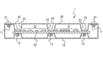
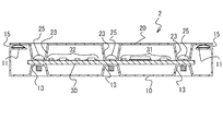
図1は、実施例1に係る筐体のシールド構造について示した図である。この図1は、筐体1の内部に配線基板30を収納したシールド装置の状態での断面図を示している。筐体1としては導電性の金属材料、例えば鋼板が採用される。表面に導電性のメッキ等を施してもよい。本実施例1の筐体1は、上部開口から載置される配線基板30を下側から支持する本体10と、この本体を上部から覆う蓋部20とにより形成されている。蓋部20は複数の固定用のネジ21により、本体10の外周に形成したフランジ部11に固定されている。すなわち、本実施例のシールド構造も従来のシールド構造と同様に、開口を有する本体10とその開口を塞ぐように配設される蓋部20とを有している。そして、複数のネジ21がノイズ放射を抑制するピッチ間隔で配置され、蓋部20が本体10上にセットされている。
FIG. 1 is a diagram illustrating the shield structure of the housing according to the first embodiment. FIG. 1 shows a cross-sectional view of a shield device in which a
そして、本実施例の本体10及び蓋部20には配線基板30側へ向けて突出した突起状の接続部が形成されている。本体10からは複数の接続部13が上方へ向けて形成され、同様に蓋部20からは複数の接続部23が下方へ向けて形成されている。すなわち、本実施例1のシールド構造では、上記接続部により配線基板30が両面(表裏面)を上下から多点で挟んだ構造となっている。特に、配線基板30上でノイズ源の1つとなるノイズを発生する電子部品(ノイズ発生部品)31、32の周辺近傍に接続部13、23を形成すると共に、配線基板30の端部(外周部)に接続部を配した形態が採用されている。これによりノイズ発生部品31、32の周辺部及び配線基板30の周部が筐体1により電気的に接続した構造が形成されている。
The
上記本体10及び蓋部20の上記接続部13、23は、例えば鋼板に絞り加工や曲げ加工を施することで、これらと一体に形成できる。そして、上下の接続部13、23を対向するように同じ位置に配置し、配線基板30を上下から挟持した構造とするのが望ましい。より具体的には、図1で示すように接続部13、23を接続用のネジ25で接続し、上下に位置する本体10と蓋部20とを電気的に接続する。
The connecting
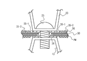
図2は、上記接続用のネジ25の周部を拡大して示した図である。配線基板30には、例えば多層配線基板であり図示のように電源線(PW)やシグナルグランド線(SG)が含まれている。この配線基板30には接続用のネジ25が通るコンタクトホール36が形成されている。このコンタクトホール36内には基板の表裏面を電気的の導通させる端子(VIA)35−1が形成されている。VIA35−1は、配線基板30上に形成されている他のパターン35−2と絶縁されている。筐体1の本体10は不図示のフレームグランド(FG)と接続されている。なお、配線基板30側のシグナルグランド(SG)は図示のようにフレームグランド(FG)とVIA35−1で直接、若しくは受動素子(抵抗、コンデンサ、インダクタ等)を介して接続される。
FIG. 2 is an enlarged view of the peripheral portion of the connecting
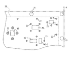
図3は、筐体1の本体10及び蓋部20に形成する接続部の配置例を模式的に示した一部平面図である。なお、図3ではノイズ発生部品をNA〜NDで例示し、これらからの放射ノイズを抑制する接続部13、23を本体10及び蓋部20で同じ位置に配置する場合を示している。図3では接続部を符号23で代表して示す。接続部23は、ノイズ発生部品からの放射ノイズを効果的に低減できるように周部に複数配置する。ノイズ発生部品NA、NBの場合のように、例えば各角部や各辺に接続部23を配置する。これら接続部23の間に更に他の接続部を配置してもよく、この場合にはノイズ低減効果を向上させることができる。
FIG. 3 is a partial plan view schematically showing an arrangement example of connection portions formed on the
また、2個のノイズ発生部品をNC−1、NC−2の外周を一体にして接続部23を配置してもよい。また、ノイズ発生部品NDのように角部に位置するときには、角部近傍に配した接続部23−Aを兼用して用いることができる。図2からも確認できるが、接続部23は一定の形状に揃える必要はない。周辺のスペースや対象とする部品の大小に応じて適宜に大きさを変化させてもよい。
Further, the connecting
以上で説明した本実施例1のシールド構造を採用すると、筐体1内において配線基板30上の部品から放射されたノイズを接続部23を介して基板30側へ戻すことができる。このような構造では、ノイズのループ面積が小さくなる。よって、従来のようにループ面積が大きくなるために筐体がアンテナとして作用しノイズを放射していた場合と比較して、筐体からのノイズ放射を確実に抑制できる。上記実施例1では、ノイズ発生部品31,32を囲むように接続部13、23を配設すると共に、配線基板30の周部に接続部13、23を配設する場合を一例として示している。しかし、ノイズ発生部品31,32の周部、又は配線基板30の周部にだけ接続部13、23を設けた場合も放射ノイズ低減の効果が得られる。
When the shield structure of the first embodiment described above is adopted, noise radiated from the components on the
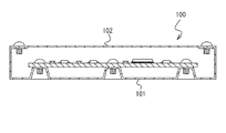
図4から図7は上記実施例1の筐体1のシールド効果を説明するために示した図である。図4は、実施例1のシールド構造による効果を確認するために作製した比較用の筐体100の構造を示した図である。この筐体100は蓋部102が接続部を有さず平板状に形成されている。他の構成は図1に示した実施例1と同様である。
4 to 7 are views for explaining the shielding effect of the
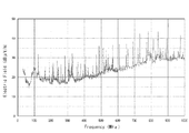
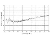
図5は、図4に示す筐体100の蓋部102を外した状態で放射ノイズの発生状態を測定した結果を示した図である。図6は、図4に示す筐体100に従来と同様に固定ネジのピッチを小さくして蓋部102を装着して放射ノイズの発生状態を測定した結果を示した図である。そして、図7は、実施例1で示した筐体1からの放射ノイズの発生状態を測定した結果を示した図である。なお、各図では横軸に周波数(Frequency(MHz))、縦軸に電界(Electric Field(dBμV/m))をとっている。
FIG. 5 is a diagram showing a result of measuring the generation state of radiation noise in a state where the
図5に示すように、蓋部102を外した状態では筐体100が全くノイズを遮蔽しないので、全帯域で配線基板から多量のノイズが放射されていることが分かる。そして、蓋部102を装着して配線基板を略密閉した空間内に収納すると図6で示すように、ノイズの放射が大幅に減少することも確認できる。この図6で示した状態が、従来において一般的に採用されていた筐体のシールド構造に相当する。しかし、図6では周波数約480MHzから約820MHzでのピークが未だに大きい。すなわち、この帯域でのノイズ放射を抑制できない。このノイズは筐体100がアンテナとして機能して放出されたものと推定される。
As shown in FIG. 5, it can be seen that a large amount of noise is radiated from the wiring board in the entire band because the
上記に対して実施例1について示す図7では、図6で示す蓋部102を装着しても抑制できなかったノイズが除去されていることを確認できる。すなわち、実施例1の筐体1によると全帯域においてピークが押えられ放射ノイズが確実に抑制されている。
In contrast to the above, in FIG. 7 showing the first embodiment, it can be confirmed that noise that could not be suppressed even when the
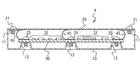
図8は、上記実施例1の変形例を示した図である。図1と同一の部位には同じ符号を付している。この変形例の筐体2は、本体10の外周部と蓋部20との間を前記の固定用のネジ21に替えて導電性を備えた板バネ15が配設されている。上下の接続部13、23が接続用のネジ25で固定されることから、本実施例2の筐体2の外周部を導電性を備えた板バネ15で接続できる。この板バネ15は、レール状に長く設定してもよいし、前述した固定用のネジの場合と同様に内部からノイズが漏洩しない狭いピッチで複数配置してもよい。また、この板バネ15に代えて、導電性及び弾性を備えたガスケットを同様に採用することができる。本変形例で示した構造を採用した場合にも、実施例1の場合と同様に筐体からの放射されるノイズを確実に抑制できる。
FIG. 8 is a view showing a modification of the first embodiment. The same parts as those in FIG. 1 are denoted by the same reference numerals. In the
図9は、実施例2に係る筐体3のシールド構造について示した図である。この図9でも、実施例1のシールド構造と同様の部位には、同一の符号を付して重複する説明を省略する。この実施例2は蓋部26が平板状であり、蓋部と一体の接続部を有していない。しかし、蓋部26と配線基板30とを電気的に接続し、接続部として機能する金属サポート40が配置されている。この金属サポート40は、例えば金属製の管状部材である。この管路内を長めの接続ネジ27が貫通しており、接続ネジ27によって蓋部26が配線基板30と接続されている。
FIG. 9 is a diagram illustrating the shield structure of the housing 3 according to the second embodiment. In FIG. 9 as well, the same parts as those of the shield structure of the first embodiment are denoted by the same reference numerals, and redundant description is omitted. In the second embodiment, the
上記金属サポート40も本体10側の接続部13と対向する位置に配置されている。すなわち、本実施例2の場合は本体10側の接続部13と蓋部20側で接続部として機能する金属サポート40とによって、配線基板30が複数の位置で挟んだ構造となる。このような構造を採用した場合にも、実施例1の場合と同様に筐体からの放射されるノイズを確実に抑制できる。なお、図9で例示しているのは、本体10に一体成形した接続部13を設け、蓋部26側に金属サポート40を採用した場合である。これとは逆に本体10側を平坦として金属サポートを用いてもよいし、上下共に金属サポートを採用してもよい。なお、本実施例2の蓋部26も、複数のネジ21によって筐体の本体10の外周上部と電気的な接続を持って固定されている。
The
図10は、実施例3に係る筐体4のシールド構造について示した図である。この図10の場合も実施例1のシールド構造と同様の部位には同一の符号を付している。本実施例3の蓋部28も平板状であり、蓋部と一体の接続部を有していない。しかし、本実施例3では蓋部26と配線基板30とを電気的に接続し、接続部として機能する導電性及び弾性を備えた板バネ45が配置されている。板バネ45は本体10の接続部13を配線基板30に接続するネジ25を利用して位置決めされている。この板バネ45は、例えば短冊状に形成したベリリウム銅を図示のように湾曲させ、上側の蓋部28と下側の配線基板30とに所定圧を持って接するように配設されている。
FIG. 10 is a diagram illustrating the shield structure of the housing 4 according to the third embodiment. In the case of FIG. 10 as well, the same parts as those of the shield structure of the first embodiment are denoted by the same reference numerals. The
上記板バネ45も本体10側の接続部13と対向する位置に配置されている。すなわち、本実施例3の場合は本体10側の接続部13と蓋部20側で接続部として機能する板バネ45とによって、配線基板30が複数の位置で挟んだ構造が実現される。このような構造を採用した場合にも、実施例1の場合と同様に筐体からの放射されるノイズを確実に抑制できる。なお、図10では板バネ45を、本体10の接続部13を配線基板30に接続するネジ25を利用して固定したがこのような態様に限らない。他の固定手段(他のネジ、カシメ、導電性接着剤等)を用いて、ノイズ発生部品の周部近傍に上記と同様の板バネを配置してもよい。
The
また、図10で例示しているのは、本体10には一体成形した接続部13を設け、蓋部26側に板バネ45を採用した場合である。これとは逆に本体10側を平坦として板バネを用いてもよいし、上下共に板バネ45を採用してもよい。なお、本実施例3の蓋部26も、複数のネジ21によって筐体の本体10の外周上部と電気的な接続を持って固定されている。
FIG. 10 illustrates the case where the
以上説明した実施例のシールド構造であれば、ノイズ発生基板を収納しても筐体がアンテナとして作用しノイズを放射するという事態を確実に防止できる。よって、電子部品を搭載した配線基板を上記実施例で示した筐体内に収納した形態で実現されるシールド装置であれば、優れたノイズシールド効果を具備しているので、周辺装置へのノイズ障害の問題を発生させない。 With the shield structure of the embodiment described above, it is possible to reliably prevent a situation in which the housing acts as an antenna and radiates noise even when the noise generating substrate is housed. Therefore, if the shield device is realized in a form in which the wiring board on which the electronic component is mounted is housed in the casing shown in the above embodiment, it has an excellent noise shielding effect, so that noise disturbance to peripheral devices is achieved. Does not cause problems.
また、前述した実施例では、筐体の本体の開口が上に形成された構造を一例として示したが、本発明は横方向から配線基板を収納する形態の筐体にも同様に適用できる。例えば図10で示した実施例3は配線基板30に板バネ45をセットして、筐体の横に形成した開口から内部に納めればよい。
In the above-described embodiments, the structure in which the opening of the main body of the housing is formed is shown as an example. However, the present invention can be similarly applied to a housing in which the wiring board is accommodated from the lateral direction. For example, in the third embodiment shown in FIG. 10, the
以上、本発明の好ましい一実施形態について詳述したが、本発明は係る特定の実施形態に限定されるものではなく、特許請求の範囲に記載された本発明の要旨の範囲内において、種々の変形・変更が可能である。 The preferred embodiment of the present invention has been described in detail above. However, the present invention is not limited to the specific embodiment, and various modifications can be made within the scope of the gist of the present invention described in the claims. Deformation / change is possible.
1 筐体
10 本体
13 接続部
20 蓋部
21 ネジ
23 接続部
25 ネジ
30 配線基板
31、32 電子部品
DESCRIPTION OF
Claims (9)
前記筐体と前記配線基板の表面及び裏面とを接続する接続部を複数備え、該接続部により前記配線基板を挟んでいることを特徴とする筐体のシールド構造。 A shield structure for a housing that houses a wiring board on which electronic components are mounted,
A shielding structure for a housing, comprising a plurality of connecting portions for connecting the housing and the front and back surfaces of the wiring board, wherein the wiring substrate is sandwiched by the connecting portions.
9. A shield device, wherein a wiring board on which an electronic component is mounted is shielded by the shield structure of the casing according to claim 1.
Priority Applications (1)
| Application Number | Priority Date | Filing Date | Title |
|---|---|---|---|
| JP2004109047A JP2005294627A (en) | 2004-04-01 | 2004-04-01 | Shield structure of case |
Applications Claiming Priority (1)
| Application Number | Priority Date | Filing Date | Title |
|---|---|---|---|
| JP2004109047A JP2005294627A (en) | 2004-04-01 | 2004-04-01 | Shield structure of case |
Publications (1)
| Publication Number | Publication Date |
|---|---|
| JP2005294627A true JP2005294627A (en) | 2005-10-20 |
Family
ID=35327205
Family Applications (1)
| Application Number | Title | Priority Date | Filing Date |
|---|---|---|---|
| JP2004109047A Pending JP2005294627A (en) | 2004-04-01 | 2004-04-01 | Shield structure of case |
Country Status (1)
| Country | Link |
|---|---|
| JP (1) | JP2005294627A (en) |
Cited By (8)
| Publication number | Priority date | Publication date | Assignee | Title |
|---|---|---|---|---|
| CN103857267A (en) * | 2012-11-30 | 2014-06-11 | 京瓷办公信息系统株式会社 | Shield structure for electronic apparatus |
| JP2016102885A (en) * | 2014-11-28 | 2016-06-02 | 京セラドキュメントソリューションズ株式会社 | Image forming apparatus |
| WO2017159531A1 (en) * | 2016-03-16 | 2017-09-21 | 株式会社ソニー・インタラクティブエンタテインメント | Electronic device |
| US10719756B2 (en) | 2016-11-15 | 2020-07-21 | Murata Manufacturing Co., Ltd. | UHF band RFID tag and UHF band RFID tagged article |
| JP2022133819A (en) * | 2021-03-02 | 2022-09-14 | マツダ株式会社 | Control unit structure |
| US11457548B2 (en) | 2018-09-25 | 2022-09-27 | Hitachi Astemo, Ltd. | Electronic control device |
| DE112021008398T5 (en) | 2021-10-26 | 2024-08-01 | Hitachi Astemo, Ltd. | ELECTRONIC CONTROL DEVICE |
| US12171071B2 (en) | 2019-11-29 | 2024-12-17 | Hitachi Astemo, Ltd. | Electronic control device |
Citations (2)
| Publication number | Priority date | Publication date | Assignee | Title |
|---|---|---|---|---|
| JP2000252676A (en) * | 1999-02-26 | 2000-09-14 | Nec Saitama Ltd | Sealed case |
| JP2003188571A (en) * | 2001-12-18 | 2003-07-04 | Nef:Kk | Printed board shielding apparatus |
-
2004
- 2004-04-01 JP JP2004109047A patent/JP2005294627A/en active Pending
Patent Citations (2)
| Publication number | Priority date | Publication date | Assignee | Title |
|---|---|---|---|---|
| JP2000252676A (en) * | 1999-02-26 | 2000-09-14 | Nec Saitama Ltd | Sealed case |
| JP2003188571A (en) * | 2001-12-18 | 2003-07-04 | Nef:Kk | Printed board shielding apparatus |
Cited By (13)
| Publication number | Priority date | Publication date | Assignee | Title |
|---|---|---|---|---|
| US9101045B2 (en) | 2012-11-30 | 2015-08-04 | Kyocera Document Solutions Inc. | Shield structure for electronic apparatus |
| CN103857267B (en) * | 2012-11-30 | 2017-01-11 | 京瓷办公信息系统株式会社 | Shield structure for electronic apparatus |
| CN103857267A (en) * | 2012-11-30 | 2014-06-11 | 京瓷办公信息系统株式会社 | Shield structure for electronic apparatus |
| JP2016102885A (en) * | 2014-11-28 | 2016-06-02 | 京セラドキュメントソリューションズ株式会社 | Image forming apparatus |
| US10966356B2 (en) | 2016-03-16 | 2021-03-30 | Sony Interactive Entertainment Inc. | Electronic apparatus |
| WO2017159531A1 (en) * | 2016-03-16 | 2017-09-21 | 株式会社ソニー・インタラクティブエンタテインメント | Electronic device |
| CN108781526A (en) * | 2016-03-16 | 2018-11-09 | 索尼互动娱乐股份有限公司 | Electronic equipment |
| US10719756B2 (en) | 2016-11-15 | 2020-07-21 | Murata Manufacturing Co., Ltd. | UHF band RFID tag and UHF band RFID tagged article |
| US11457548B2 (en) | 2018-09-25 | 2022-09-27 | Hitachi Astemo, Ltd. | Electronic control device |
| US12171071B2 (en) | 2019-11-29 | 2024-12-17 | Hitachi Astemo, Ltd. | Electronic control device |
| JP2022133819A (en) * | 2021-03-02 | 2022-09-14 | マツダ株式会社 | Control unit structure |
| JP7567557B2 (en) | 2021-03-02 | 2024-10-16 | マツダ株式会社 | Control unit structure |
| DE112021008398T5 (en) | 2021-10-26 | 2024-08-01 | Hitachi Astemo, Ltd. | ELECTRONIC CONTROL DEVICE |
Similar Documents
| Publication | Publication Date | Title |
|---|---|---|
| US20090268420A1 (en) | Shielding assembly | |
| JP2017158223A (en) | Electric motor control device | |
| JP2009158838A (en) | Electronics | |
| JP2005294627A (en) | Shield structure of case | |
| JP2008176567A (en) | Printed circuit board assembly, casing for information technology device, and information technology device | |
| US20090147494A1 (en) | Electronic device and slot | |
| JP2009272499A (en) | Electronic control unit | |
| US20130044419A1 (en) | Electronic device | |
| JPH0786786A (en) | LSI case shield structure | |
| JP5949374B2 (en) | Electronics | |
| JP5294353B2 (en) | Electromagnetic shielding structure | |
| JP5022800B2 (en) | Electronics | |
| TW200922439A (en) | Electronic circuit mould | |
| JP2010080691A (en) | Shielding structure and electronic apparatus | |
| JP3094771B2 (en) | Electronic and communication equipment unit structure | |
| JP2013254925A (en) | Electronic circuit device | |
| EP2239779B1 (en) | Flexible image-sensing module with anti-EMI function | |
| JP5257326B2 (en) | Portable terminal | |
| JP2010267928A (en) | Electronic device | |
| JP2001007589A (en) | Shielding structure for printed-board power device | |
| JPWO2009063734A1 (en) | Electronic component mounting equipment | |
| CN107528118A (en) | Communication device and antenna assembly thereof | |
| JP2007123722A (en) | Shield structure | |
| JP4205720B2 (en) | Card device | |
| JP2014056760A (en) | Electronic apparatus |
Legal Events
| Date | Code | Title | Description |
|---|---|---|---|
| A621 | Written request for application examination |
Free format text: JAPANESE INTERMEDIATE CODE: A621 Effective date: 20070322 |
|
| A977 | Report on retrieval |
Free format text: JAPANESE INTERMEDIATE CODE: A971007 Effective date: 20090528 |
|
| A131 | Notification of reasons for refusal |
Free format text: JAPANESE INTERMEDIATE CODE: A131 Effective date: 20090609 |
|
| A521 | Written amendment |
Effective date: 20090807 Free format text: JAPANESE INTERMEDIATE CODE: A523 |
|
| A131 | Notification of reasons for refusal |
Effective date: 20090915 Free format text: JAPANESE INTERMEDIATE CODE: A131 |
|
| RD13 | Notification of appointment of power of sub attorney |
Free format text: JAPANESE INTERMEDIATE CODE: A7433 Effective date: 20091110 |
|
| A521 | Written amendment |
Effective date: 20091116 Free format text: JAPANESE INTERMEDIATE CODE: A523 |
|
| A02 | Decision of refusal |
Free format text: JAPANESE INTERMEDIATE CODE: A02 Effective date: 20091222 |
|
| A521 | Written amendment |
Free format text: JAPANESE INTERMEDIATE CODE: A523 Effective date: 20100319 |
|
| A911 | Transfer of reconsideration by examiner before appeal (zenchi) |
Free format text: JAPANESE INTERMEDIATE CODE: A911 Effective date: 20100416 |
|
| A912 | Removal of reconsideration by examiner before appeal (zenchi) |
Effective date: 20100514 Free format text: JAPANESE INTERMEDIATE CODE: A912 |