JP2005101187A - フレキシブル配線基板、液晶装置、電気光学装置および電子機器 - Google Patents
フレキシブル配線基板、液晶装置、電気光学装置および電子機器 Download PDFInfo
- Publication number
- JP2005101187A JP2005101187A JP2003331690A JP2003331690A JP2005101187A JP 2005101187 A JP2005101187 A JP 2005101187A JP 2003331690 A JP2003331690 A JP 2003331690A JP 2003331690 A JP2003331690 A JP 2003331690A JP 2005101187 A JP2005101187 A JP 2005101187A
- Authority
- JP
- Japan
- Prior art keywords
- land
- liquid crystal
- wiring board
- flexible wiring
- light emitting
- Prior art date
- Legal status (The legal status is an assumption and is not a legal conclusion. Google has not performed a legal analysis and makes no representation as to the accuracy of the status listed.)
- Withdrawn
Links
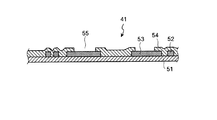
- 239000004973 liquid crystal related substance Substances 0.000 title claims description 56
- 239000000758 substrate Substances 0.000 claims abstract description 23
- 230000001681 protective effect Effects 0.000 claims abstract description 11
- 230000002093 peripheral effect Effects 0.000 claims abstract description 4
- 239000000382 optic material Substances 0.000 claims 1
- 239000000463 material Substances 0.000 abstract description 9
- 229910000679 solder Inorganic materials 0.000 description 13
- 230000000694 effects Effects 0.000 description 7
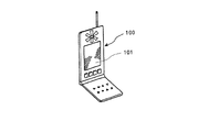
- 230000010365 information processing Effects 0.000 description 4
- 238000010586 diagram Methods 0.000 description 2
- 238000006073 displacement reaction Methods 0.000 description 2
- 239000003566 sealing material Substances 0.000 description 2
- 238000005452 bending Methods 0.000 description 1
- 230000001413 cellular effect Effects 0.000 description 1
- 239000004020 conductor Substances 0.000 description 1
- 230000001747 exhibiting effect Effects 0.000 description 1
- 239000011810 insulating material Substances 0.000 description 1
- 230000001678 irradiating effect Effects 0.000 description 1
- 239000011159 matrix material Substances 0.000 description 1
- 230000003287 optical effect Effects 0.000 description 1
- 230000005693 optoelectronics Effects 0.000 description 1
Images


Landscapes
- Liquid Crystal (AREA)
- Devices For Indicating Variable Information By Combining Individual Elements (AREA)
- Electric Connection Of Electric Components To Printed Circuits (AREA)
Priority Applications (1)
| Application Number | Priority Date | Filing Date | Title |
|---|---|---|---|
| JP2003331690A JP2005101187A (ja) | 2003-09-24 | 2003-09-24 | フレキシブル配線基板、液晶装置、電気光学装置および電子機器 |
Applications Claiming Priority (1)
| Application Number | Priority Date | Filing Date | Title |
|---|---|---|---|
| JP2003331690A JP2005101187A (ja) | 2003-09-24 | 2003-09-24 | フレキシブル配線基板、液晶装置、電気光学装置および電子機器 |
Publications (2)
| Publication Number | Publication Date |
|---|---|
| JP2005101187A true JP2005101187A (ja) | 2005-04-14 |
| JP2005101187A5 JP2005101187A5 (enExample) | 2006-05-18 |
Family
ID=34460277
Family Applications (1)
| Application Number | Title | Priority Date | Filing Date |
|---|---|---|---|
| JP2003331690A Withdrawn JP2005101187A (ja) | 2003-09-24 | 2003-09-24 | フレキシブル配線基板、液晶装置、電気光学装置および電子機器 |
Country Status (1)
| Country | Link |
|---|---|
| JP (1) | JP2005101187A (enExample) |
Cited By (5)
| Publication number | Priority date | Publication date | Assignee | Title |
|---|---|---|---|---|
| JP2008140596A (ja) * | 2006-11-30 | 2008-06-19 | Minebea Co Ltd | 面状照明装置 |
| JP2013149511A (ja) * | 2012-01-20 | 2013-08-01 | Minebea Co Ltd | 面状照明装置 |
| JP2016126972A (ja) * | 2015-01-07 | 2016-07-11 | ミネベア株式会社 | 面状照明装置 |
| JP2016189348A (ja) * | 2016-07-08 | 2016-11-04 | ミネベア株式会社 | 面状照明装置 |
| WO2017138381A1 (ja) * | 2016-02-10 | 2017-08-17 | 株式会社村田製作所 | フレキシブルケーブル付電子部品連およびフレキシブルケーブル付電子部品連の製造方法 |
-
2003
- 2003-09-24 JP JP2003331690A patent/JP2005101187A/ja not_active Withdrawn
Cited By (10)
| Publication number | Priority date | Publication date | Assignee | Title |
|---|---|---|---|---|
| JP2008140596A (ja) * | 2006-11-30 | 2008-06-19 | Minebea Co Ltd | 面状照明装置 |
| JP2013149511A (ja) * | 2012-01-20 | 2013-08-01 | Minebea Co Ltd | 面状照明装置 |
| US9383086B2 (en) | 2012-01-20 | 2016-07-05 | Minebea Co., Ltd. | Planar lighting device and mounting substrate including conduction pattern with extension parts |
| US10028382B2 (en) | 2012-01-20 | 2018-07-17 | Minebea Co., Ltd. | Planar lighting device and mounting substrate including conduction pattern with extension parts |
| JP2016126972A (ja) * | 2015-01-07 | 2016-07-11 | ミネベア株式会社 | 面状照明装置 |
| CN105757614A (zh) * | 2015-01-07 | 2016-07-13 | 美蓓亚株式会社 | 面状照明装置 |
| US10139552B2 (en) | 2015-01-07 | 2018-11-27 | Minebea Mitsumi Inc. | Planar lighting device having light sources with electrode terminals and mounting substrate with conductive pattern including a plurality of lands together having relative spacing between the lands and electrode terminals |
| CN105757614B (zh) * | 2015-01-07 | 2019-05-07 | 美蓓亚株式会社 | 面状照明装置 |
| WO2017138381A1 (ja) * | 2016-02-10 | 2017-08-17 | 株式会社村田製作所 | フレキシブルケーブル付電子部品連およびフレキシブルケーブル付電子部品連の製造方法 |
| JP2016189348A (ja) * | 2016-07-08 | 2016-11-04 | ミネベア株式会社 | 面状照明装置 |
Similar Documents
| Publication | Publication Date | Title |
|---|---|---|
| US12016134B2 (en) | Notched display layers | |
| US7663726B2 (en) | Liquid crystal apparatus and electronic apparatus | |
| JP4306590B2 (ja) | 電気光学装置及び電子機器 | |
| KR100433354B1 (ko) | 액정표시장치및그것의사용기기 | |
| US11054570B2 (en) | Liquid crystal display device having a joint portion of a wiring substrate extending from an inside to an outside of the case | |
| KR20140029196A (ko) | 드라이버 회로 선반이 감소된 디스플레이 | |
| US6831841B2 (en) | Flexible substrate, electro-optical device and electronic device | |
| JP2008165179A (ja) | 液晶装置、電子機器 | |
| KR20210027703A (ko) | 표시 장치 | |
| JP4525065B2 (ja) | 電気光学装置及びその製造方法、電子機器 | |
| US20080123335A1 (en) | Printed circuit board assembly and display having the same | |
| JP2009216810A (ja) | 電気光学装置及び電子機器 | |
| JP2005183536A (ja) | フレキシブル配線基板、電気光学装置及び電子機器 | |
| JP2006058741A (ja) | 液晶表示装置 | |
| JP2005101187A (ja) | フレキシブル配線基板、液晶装置、電気光学装置および電子機器 | |
| JP7083683B2 (ja) | 液晶表示装置 | |
| JP4297021B2 (ja) | 電気光学装置、照明装置及び電子機器 | |
| KR101578215B1 (ko) | 백라이트 유닛 및 이를 구비한 액정표시장치 | |
| JP4519709B2 (ja) | フレキシブル配線基板、電子部品搭載フレキシブル配線基板、および液晶表示装置 | |
| JP4432569B2 (ja) | 電気光学装置及び電子機器 | |
| JP2008159873A (ja) | フレキシブルプリント配線基板およびその製造方法、電気光学装置および電子機器 | |
| JP2004152984A (ja) | 配線基板、電気光学装置及び電子機器 | |
| KR20080041994A (ko) | 인쇄회로기판 조립체 및 이를 구비한 표시 장치 | |
| JP3653981B2 (ja) | 液晶装置の実装構造及び電子機器 | |
| JP2007133281A (ja) | 表示装置 |
Legal Events
| Date | Code | Title | Description |
|---|---|---|---|
| A521 | Written amendment |
Free format text: JAPANESE INTERMEDIATE CODE: A523 Effective date: 20060329 |
|
| A621 | Written request for application examination |
Free format text: JAPANESE INTERMEDIATE CODE: A621 Effective date: 20060329 |
|
| RD04 | Notification of resignation of power of attorney |
Free format text: JAPANESE INTERMEDIATE CODE: A7424 Effective date: 20070403 |
|
| A977 | Report on retrieval |
Free format text: JAPANESE INTERMEDIATE CODE: A971007 Effective date: 20081031 |
|
| A131 | Notification of reasons for refusal |
Free format text: JAPANESE INTERMEDIATE CODE: A131 Effective date: 20081216 |
|
| A761 | Written withdrawal of application |
Free format text: JAPANESE INTERMEDIATE CODE: A761 Effective date: 20090209 |