JP2004111928A - 半導体デバイスの常誘電性材料及びその製造方法 - Google Patents
半導体デバイスの常誘電性材料及びその製造方法 Download PDFInfo
- Publication number
- JP2004111928A JP2004111928A JP2003286413A JP2003286413A JP2004111928A JP 2004111928 A JP2004111928 A JP 2004111928A JP 2003286413 A JP2003286413 A JP 2003286413A JP 2003286413 A JP2003286413 A JP 2003286413A JP 2004111928 A JP2004111928 A JP 2004111928A
- Authority
- JP
- Japan
- Prior art keywords
- seed layer
- layer
- depositing
- ferroelectric
- paraelectric
- Prior art date
- Legal status (The legal status is an assumption and is not a legal conclusion. Google has not performed a legal analysis and makes no representation as to the accuracy of the status listed.)
- Pending
Links
Images


Classifications
-
- C—CHEMISTRY; METALLURGY
- C23—COATING METALLIC MATERIAL; COATING MATERIAL WITH METALLIC MATERIAL; CHEMICAL SURFACE TREATMENT; DIFFUSION TREATMENT OF METALLIC MATERIAL; COATING BY VACUUM EVAPORATION, BY SPUTTERING, BY ION IMPLANTATION OR BY CHEMICAL VAPOUR DEPOSITION, IN GENERAL; INHIBITING CORROSION OF METALLIC MATERIAL OR INCRUSTATION IN GENERAL
- C23C—COATING METALLIC MATERIAL; COATING MATERIAL WITH METALLIC MATERIAL; SURFACE TREATMENT OF METALLIC MATERIAL BY DIFFUSION INTO THE SURFACE, BY CHEMICAL CONVERSION OR SUBSTITUTION; COATING BY VACUUM EVAPORATION, BY SPUTTERING, BY ION IMPLANTATION OR BY CHEMICAL VAPOUR DEPOSITION, IN GENERAL
- C23C16/00—Chemical coating by decomposition of gaseous compounds, without leaving reaction products of surface material in the coating, i.e. chemical vapour deposition [CVD] processes
- C23C16/02—Pretreatment of the material to be coated
- C23C16/0272—Deposition of sub-layers, e.g. to promote the adhesion of the main coating
-
- H—ELECTRICITY
- H10—SEMICONDUCTOR DEVICES; ELECTRIC SOLID-STATE DEVICES NOT OTHERWISE PROVIDED FOR
- H10D—INORGANIC ELECTRIC SEMICONDUCTOR DEVICES
- H10D84/00—Integrated devices formed in or on semiconductor substrates that comprise only semiconducting layers, e.g. on Si wafers or on GaAs-on-Si wafers
-
- H—ELECTRICITY
- H10—SEMICONDUCTOR DEVICES; ELECTRIC SOLID-STATE DEVICES NOT OTHERWISE PROVIDED FOR
- H10P—GENERIC PROCESSES OR APPARATUS FOR THE MANUFACTURE OR TREATMENT OF DEVICES COVERED BY CLASS H10
- H10P14/00—Formation of materials, e.g. in the shape of layers or pillars
- H10P14/60—Formation of materials, e.g. in the shape of layers or pillars of insulating materials
- H10P14/69—Inorganic materials
- H10P14/692—Inorganic materials composed of oxides, glassy oxides or oxide-based glasses
- H10P14/6938—Inorganic materials composed of oxides, glassy oxides or oxide-based glasses the material containing at least one metal element, e.g. metal oxides, metal oxynitrides or metal oxycarbides
- H10P14/69398—Inorganic materials composed of oxides, glassy oxides or oxide-based glasses the material containing at least one metal element, e.g. metal oxides, metal oxynitrides or metal oxycarbides the material having a perovskite structure, e.g. BaTiO3
-
- C—CHEMISTRY; METALLURGY
- C23—COATING METALLIC MATERIAL; COATING MATERIAL WITH METALLIC MATERIAL; CHEMICAL SURFACE TREATMENT; DIFFUSION TREATMENT OF METALLIC MATERIAL; COATING BY VACUUM EVAPORATION, BY SPUTTERING, BY ION IMPLANTATION OR BY CHEMICAL VAPOUR DEPOSITION, IN GENERAL; INHIBITING CORROSION OF METALLIC MATERIAL OR INCRUSTATION IN GENERAL
- C23C—COATING METALLIC MATERIAL; COATING MATERIAL WITH METALLIC MATERIAL; SURFACE TREATMENT OF METALLIC MATERIAL BY DIFFUSION INTO THE SURFACE, BY CHEMICAL CONVERSION OR SUBSTITUTION; COATING BY VACUUM EVAPORATION, BY SPUTTERING, BY ION IMPLANTATION OR BY CHEMICAL VAPOUR DEPOSITION, IN GENERAL
- C23C16/00—Chemical coating by decomposition of gaseous compounds, without leaving reaction products of surface material in the coating, i.e. chemical vapour deposition [CVD] processes
- C23C16/22—Chemical coating by decomposition of gaseous compounds, without leaving reaction products of surface material in the coating, i.e. chemical vapour deposition [CVD] processes characterised by the deposition of inorganic material, other than metallic material
- C23C16/30—Deposition of compounds, mixtures or solid solutions, e.g. borides, carbides, nitrides
- C23C16/40—Oxides
- C23C16/409—Oxides of the type ABO3 with A representing alkali, alkaline earth metal or lead and B representing a refractory metal, nickel, scandium or a lanthanide
-
- H—ELECTRICITY
- H10—SEMICONDUCTOR DEVICES; ELECTRIC SOLID-STATE DEVICES NOT OTHERWISE PROVIDED FOR
- H10B—ELECTRONIC MEMORY DEVICES
- H10B53/00—Ferroelectric RAM [FeRAM] devices comprising ferroelectric memory capacitors
-
- H—ELECTRICITY
- H10—SEMICONDUCTOR DEVICES; ELECTRIC SOLID-STATE DEVICES NOT OTHERWISE PROVIDED FOR
- H10B—ELECTRONIC MEMORY DEVICES
- H10B53/00—Ferroelectric RAM [FeRAM] devices comprising ferroelectric memory capacitors
- H10B53/30—Ferroelectric RAM [FeRAM] devices comprising ferroelectric memory capacitors characterised by the memory core region
-
- H—ELECTRICITY
- H10—SEMICONDUCTOR DEVICES; ELECTRIC SOLID-STATE DEVICES NOT OTHERWISE PROVIDED FOR
- H10D—INORGANIC ELECTRIC SEMICONDUCTOR DEVICES
- H10D1/00—Resistors, capacitors or inductors
- H10D1/60—Capacitors
- H10D1/68—Capacitors having no potential barriers
- H10D1/682—Capacitors having no potential barriers having dielectrics comprising perovskite structures
- H10D1/684—Capacitors having no potential barriers having dielectrics comprising perovskite structures the dielectrics comprising multiple layers, e.g. comprising buffer layers, seed layers or gradient layers
Landscapes
- Chemical & Material Sciences (AREA)
- General Chemical & Material Sciences (AREA)
- Chemical Kinetics & Catalysis (AREA)
- Engineering & Computer Science (AREA)
- Materials Engineering (AREA)
- Mechanical Engineering (AREA)
- Metallurgy (AREA)
- Organic Chemistry (AREA)
- Inorganic Chemistry (AREA)
- Semiconductor Memories (AREA)
- Chemical Vapour Deposition (AREA)
- Formation Of Insulating Films (AREA)
Applications Claiming Priority (1)
| Application Number | Priority Date | Filing Date | Title |
|---|---|---|---|
| US10/212,895 US20040023416A1 (en) | 2002-08-05 | 2002-08-05 | Method for forming a paraelectric semiconductor device |
Publications (2)
| Publication Number | Publication Date |
|---|---|
| JP2004111928A true JP2004111928A (ja) | 2004-04-08 |
| JP2004111928A5 JP2004111928A5 (enExample) | 2006-09-07 |
Family
ID=31187833
Family Applications (1)
| Application Number | Title | Priority Date | Filing Date |
|---|---|---|---|
| JP2003286413A Pending JP2004111928A (ja) | 2002-08-05 | 2003-08-05 | 半導体デバイスの常誘電性材料及びその製造方法 |
Country Status (4)
| Country | Link |
|---|---|
| US (1) | US20040023416A1 (enExample) |
| JP (1) | JP2004111928A (enExample) |
| KR (1) | KR20040014283A (enExample) |
| DE (1) | DE10328872A1 (enExample) |
Cited By (2)
| Publication number | Priority date | Publication date | Assignee | Title |
|---|---|---|---|---|
| JP2014520404A (ja) * | 2011-06-20 | 2014-08-21 | アドバンスド テクノロジー マテリアルズ,インコーポレイテッド | 高誘電率ペロブスカイト材料ならびにその作製および使用方法 |
| JP2016515162A (ja) * | 2013-02-11 | 2016-05-26 | 日本テキサス・インスツルメンツ株式会社 | 強誘電性誘電材料の多段階堆積 |
Families Citing this family (5)
| Publication number | Priority date | Publication date | Assignee | Title |
|---|---|---|---|---|
| KR100660550B1 (ko) * | 2005-09-15 | 2006-12-22 | 삼성전자주식회사 | 강유전체막 및 강유전체 커패시터 형성 방법 |
| US8445913B2 (en) | 2007-10-30 | 2013-05-21 | Spansion Llc | Metal-insulator-metal (MIM) device and method of formation thereof |
| WO2012078488A1 (en) * | 2010-12-06 | 2012-06-14 | 3M Innovative Properties Company | Composite diode, electronic device, and methods of making the same |
| US11690228B2 (en) * | 2021-02-25 | 2023-06-27 | Taiwan Semiconductor Manufacturing Company, Ltd. | Annealed seed layer to improve ferroelectric properties of memory layer |
| FR3157226A1 (fr) * | 2023-12-21 | 2025-06-27 | Novatreat | Dispositif de préparation d’un pré-mélange gazeux, unité de flammage et procédé utilisant ce dispositif |
Family Cites Families (10)
| Publication number | Priority date | Publication date | Assignee | Title |
|---|---|---|---|---|
| JP3209082B2 (ja) * | 1996-03-06 | 2001-09-17 | セイコーエプソン株式会社 | 圧電体薄膜素子及びその製造方法、並びにこれを用いたインクジェット式記録ヘッド |
| KR0183868B1 (ko) * | 1996-05-25 | 1999-04-15 | 김광호 | 강유전체막 및 그의 형성방법 |
| JP3207206B2 (ja) * | 1996-07-17 | 2001-09-10 | シチズン時計株式会社 | 強誘電体素子及びその製造方法 |
| US5876503A (en) * | 1996-11-27 | 1999-03-02 | Advanced Technology Materials, Inc. | Multiple vaporizer reagent supply system for chemical vapor deposition utilizing dissimilar precursor compositions |
| US6190728B1 (en) * | 1997-09-29 | 2001-02-20 | Yazaki Corporation | Process for forming thin films of functional ceramics |
| US6180420B1 (en) * | 1997-12-10 | 2001-01-30 | Advanced Technology Materials, Inc. | Low temperature CVD processes for preparing ferroelectric films using Bi carboxylates |
| KR100275726B1 (ko) * | 1997-12-31 | 2000-12-15 | 윤종용 | 강유전체 메모리 장치 및 그 제조 방법 |
| EP1145293A1 (en) * | 1998-11-30 | 2001-10-17 | Interuniversitair Micro-Elektronica Centrum | Method of fabrication of a ferro-electric capacitor and method of growing a pzt layer on a substrate |
| US6316797B1 (en) * | 1999-02-19 | 2001-11-13 | Advanced Technology Materials, Inc. | Scalable lead zirconium titanate(PZT) thin film material and deposition method, and ferroelectric memory device structures comprising such thin film material |
| US6730354B2 (en) * | 2001-08-08 | 2004-05-04 | Agilent Technologies, Inc. | Forming ferroelectric Pb(Zr,Ti)O3 films |
-
2002
- 2002-08-05 US US10/212,895 patent/US20040023416A1/en not_active Abandoned
-
2003
- 2003-06-26 DE DE10328872A patent/DE10328872A1/de not_active Withdrawn
- 2003-08-05 JP JP2003286413A patent/JP2004111928A/ja active Pending
- 2003-08-05 KR KR1020030054170A patent/KR20040014283A/ko not_active Ceased
Cited By (2)
| Publication number | Priority date | Publication date | Assignee | Title |
|---|---|---|---|---|
| JP2014520404A (ja) * | 2011-06-20 | 2014-08-21 | アドバンスド テクノロジー マテリアルズ,インコーポレイテッド | 高誘電率ペロブスカイト材料ならびにその作製および使用方法 |
| JP2016515162A (ja) * | 2013-02-11 | 2016-05-26 | 日本テキサス・インスツルメンツ株式会社 | 強誘電性誘電材料の多段階堆積 |
Also Published As
| Publication number | Publication date |
|---|---|
| DE10328872A1 (de) | 2004-02-26 |
| KR20040014283A (ko) | 2004-02-14 |
| US20040023416A1 (en) | 2004-02-05 |
Similar Documents
| Publication | Publication Date | Title |
|---|---|---|
| US7459318B2 (en) | Ferroelectric and high dielectric constant integrated circuit capacitors with three-dimensional orientation for high-density memories, and method of making the same | |
| US7585683B2 (en) | Methods of fabricating ferroelectric devices | |
| US5686151A (en) | Method of forming a metal oxide film | |
| US20050019960A1 (en) | Method and apparatus for forming a ferroelectric layer | |
| US20060124987A1 (en) | Capacitor of semiconductor device and method for manufacturing the same | |
| US20010026988A1 (en) | Method of manufacturing semiconductor devices utilizing underlayer-dependency of deposition of capacitor electrode film, and semiconductor device | |
| US20120276659A1 (en) | Semiconductor device and manufacturing method thereof | |
| JP3109485B2 (ja) | 金属酸化物誘電体膜の気相成長方法 | |
| US8664011B2 (en) | Semiconductor device and method of manufacturing the semiconductor device | |
| JP3971645B2 (ja) | 半導体装置の製造方法 | |
| US8962350B2 (en) | Multi-step deposition of ferroelectric dielectric material | |
| JP5655585B2 (ja) | 半導体装置の製造方法 | |
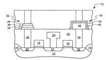
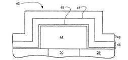
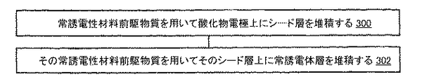
| JP2004111928A (ja) | 半導体デバイスの常誘電性材料及びその製造方法 | |
| US6495412B1 (en) | Semiconductor device having a ferroelectric capacitor and a fabrication process thereof | |
| JP4616830B2 (ja) | 半導体装置の製造方法 | |
| US6790678B2 (en) | Method for forming capacitor of ferroelectric random access memory | |
| JP2002198495A (ja) | 半導体装置およびその製造方法 | |
| KR100942958B1 (ko) | 박막 형성방법 및 이를 이용한 반도체 소자의 커패시터형성방법 | |
| US20070058415A1 (en) | Method for depositing ferroelectric thin films using a mixed oxidant gas | |
| JP2007081410A (ja) | 強誘電体膜及び強誘電体キャパシタ形成方法及び強誘電体キャパシタ | |
| US6884674B2 (en) | Method for fabricating a semiconductor device including a capacitance insulating film having a perovskite structure | |
| JP2004080020A (ja) | 強誘電性半導体デバイスを形成するための方法 | |
| JP5360023B2 (ja) | 半導体装置及びその製造方法 | |
| JP2011129719A (ja) | 半導体装置およびその製造方法 | |
| KR20080019980A (ko) | 강유전체 커패시터를 포함하는 반도체 장치의 제조 방법 |
Legal Events
| Date | Code | Title | Description |
|---|---|---|---|
| A521 | Request for written amendment filed |
Free format text: JAPANESE INTERMEDIATE CODE: A523 Effective date: 20060726 |
|
| A621 | Written request for application examination |
Free format text: JAPANESE INTERMEDIATE CODE: A621 Effective date: 20060726 |
|
| A977 | Report on retrieval |
Free format text: JAPANESE INTERMEDIATE CODE: A971007 Effective date: 20090410 |
|
| A131 | Notification of reasons for refusal |
Free format text: JAPANESE INTERMEDIATE CODE: A131 Effective date: 20090414 |
|
| A02 | Decision of refusal |
Free format text: JAPANESE INTERMEDIATE CODE: A02 Effective date: 20091110 |