EP4579715A1 - Film forming method, film forming device, susceptor, and a-gallium oxide film - Google Patents
Film forming method, film forming device, susceptor, and a-gallium oxide film Download PDFInfo
- Publication number
- EP4579715A1 EP4579715A1 EP23857247.3A EP23857247A EP4579715A1 EP 4579715 A1 EP4579715 A1 EP 4579715A1 EP 23857247 A EP23857247 A EP 23857247A EP 4579715 A1 EP4579715 A1 EP 4579715A1
- Authority
- EP
- European Patent Office
- Prior art keywords
- film
- substrate
- gas mixture
- less
- smooth section
- Prior art date
- Legal status (The legal status is an assumption and is not a legal conclusion. Google has not performed a legal analysis and makes no representation as to the accuracy of the status listed.)
- Pending
Links
Images


Classifications
-
- C—CHEMISTRY; METALLURGY
- C30—CRYSTAL GROWTH
- C30B—SINGLE-CRYSTAL GROWTH; UNIDIRECTIONAL SOLIDIFICATION OF EUTECTIC MATERIAL OR UNIDIRECTIONAL DEMIXING OF EUTECTOID MATERIAL; REFINING BY ZONE-MELTING OF MATERIAL; PRODUCTION OF A HOMOGENEOUS POLYCRYSTALLINE MATERIAL WITH DEFINED STRUCTURE; SINGLE CRYSTALS OR HOMOGENEOUS POLYCRYSTALLINE MATERIAL WITH DEFINED STRUCTURE; AFTER-TREATMENT OF SINGLE CRYSTALS OR A HOMOGENEOUS POLYCRYSTALLINE MATERIAL WITH DEFINED STRUCTURE; APPARATUS THEREFOR
- C30B29/00—Single crystals or homogeneous polycrystalline material with defined structure characterised by the material or by their shape
- C30B29/10—Inorganic compounds or compositions
- C30B29/16—Oxides
-
- C—CHEMISTRY; METALLURGY
- C23—COATING METALLIC MATERIAL; COATING MATERIAL WITH METALLIC MATERIAL; CHEMICAL SURFACE TREATMENT; DIFFUSION TREATMENT OF METALLIC MATERIAL; COATING BY VACUUM EVAPORATION, BY SPUTTERING, BY ION IMPLANTATION OR BY CHEMICAL VAPOUR DEPOSITION, IN GENERAL; INHIBITING CORROSION OF METALLIC MATERIAL OR INCRUSTATION IN GENERAL
- C23C—COATING METALLIC MATERIAL; COATING MATERIAL WITH METALLIC MATERIAL; SURFACE TREATMENT OF METALLIC MATERIAL BY DIFFUSION INTO THE SURFACE, BY CHEMICAL CONVERSION OR SUBSTITUTION; COATING BY VACUUM EVAPORATION, BY SPUTTERING, BY ION IMPLANTATION OR BY CHEMICAL VAPOUR DEPOSITION, IN GENERAL
- C23C16/00—Chemical coating by decomposition of gaseous compounds, without leaving reaction products of surface material in the coating, i.e. chemical vapour deposition [CVD] processes
- C23C16/22—Chemical coating by decomposition of gaseous compounds, without leaving reaction products of surface material in the coating, i.e. chemical vapour deposition [CVD] processes characterised by the deposition of inorganic material, other than metallic material
- C23C16/30—Deposition of compounds, mixtures or solid solutions, e.g. borides, carbides, nitrides
- C23C16/40—Oxides
-
- C—CHEMISTRY; METALLURGY
- C23—COATING METALLIC MATERIAL; COATING MATERIAL WITH METALLIC MATERIAL; CHEMICAL SURFACE TREATMENT; DIFFUSION TREATMENT OF METALLIC MATERIAL; COATING BY VACUUM EVAPORATION, BY SPUTTERING, BY ION IMPLANTATION OR BY CHEMICAL VAPOUR DEPOSITION, IN GENERAL; INHIBITING CORROSION OF METALLIC MATERIAL OR INCRUSTATION IN GENERAL
- C23C—COATING METALLIC MATERIAL; COATING MATERIAL WITH METALLIC MATERIAL; SURFACE TREATMENT OF METALLIC MATERIAL BY DIFFUSION INTO THE SURFACE, BY CHEMICAL CONVERSION OR SUBSTITUTION; COATING BY VACUUM EVAPORATION, BY SPUTTERING, BY ION IMPLANTATION OR BY CHEMICAL VAPOUR DEPOSITION, IN GENERAL
- C23C16/00—Chemical coating by decomposition of gaseous compounds, without leaving reaction products of surface material in the coating, i.e. chemical vapour deposition [CVD] processes
- C23C16/44—Chemical coating by decomposition of gaseous compounds, without leaving reaction products of surface material in the coating, i.e. chemical vapour deposition [CVD] processes characterised by the method of coating
- C23C16/4412—Details relating to the exhausts, e.g. pumps, filters, scrubbers, particle traps
-
- C—CHEMISTRY; METALLURGY
- C23—COATING METALLIC MATERIAL; COATING MATERIAL WITH METALLIC MATERIAL; CHEMICAL SURFACE TREATMENT; DIFFUSION TREATMENT OF METALLIC MATERIAL; COATING BY VACUUM EVAPORATION, BY SPUTTERING, BY ION IMPLANTATION OR BY CHEMICAL VAPOUR DEPOSITION, IN GENERAL; INHIBITING CORROSION OF METALLIC MATERIAL OR INCRUSTATION IN GENERAL
- C23C—COATING METALLIC MATERIAL; COATING MATERIAL WITH METALLIC MATERIAL; SURFACE TREATMENT OF METALLIC MATERIAL BY DIFFUSION INTO THE SURFACE, BY CHEMICAL CONVERSION OR SUBSTITUTION; COATING BY VACUUM EVAPORATION, BY SPUTTERING, BY ION IMPLANTATION OR BY CHEMICAL VAPOUR DEPOSITION, IN GENERAL
- C23C16/00—Chemical coating by decomposition of gaseous compounds, without leaving reaction products of surface material in the coating, i.e. chemical vapour deposition [CVD] processes
- C23C16/44—Chemical coating by decomposition of gaseous compounds, without leaving reaction products of surface material in the coating, i.e. chemical vapour deposition [CVD] processes characterised by the method of coating
- C23C16/448—Chemical coating by decomposition of gaseous compounds, without leaving reaction products of surface material in the coating, i.e. chemical vapour deposition [CVD] processes characterised by the method of coating characterised by the method used for generating reactive gas streams, e.g. by evaporation or sublimation of precursor materials
- C23C16/4481—Chemical coating by decomposition of gaseous compounds, without leaving reaction products of surface material in the coating, i.e. chemical vapour deposition [CVD] processes characterised by the method of coating characterised by the method used for generating reactive gas streams, e.g. by evaporation or sublimation of precursor materials by evaporation using carrier gas in contact with the source material
-
- C—CHEMISTRY; METALLURGY
- C23—COATING METALLIC MATERIAL; COATING MATERIAL WITH METALLIC MATERIAL; CHEMICAL SURFACE TREATMENT; DIFFUSION TREATMENT OF METALLIC MATERIAL; COATING BY VACUUM EVAPORATION, BY SPUTTERING, BY ION IMPLANTATION OR BY CHEMICAL VAPOUR DEPOSITION, IN GENERAL; INHIBITING CORROSION OF METALLIC MATERIAL OR INCRUSTATION IN GENERAL
- C23C—COATING METALLIC MATERIAL; COATING MATERIAL WITH METALLIC MATERIAL; SURFACE TREATMENT OF METALLIC MATERIAL BY DIFFUSION INTO THE SURFACE, BY CHEMICAL CONVERSION OR SUBSTITUTION; COATING BY VACUUM EVAPORATION, BY SPUTTERING, BY ION IMPLANTATION OR BY CHEMICAL VAPOUR DEPOSITION, IN GENERAL
- C23C16/00—Chemical coating by decomposition of gaseous compounds, without leaving reaction products of surface material in the coating, i.e. chemical vapour deposition [CVD] processes
- C23C16/44—Chemical coating by decomposition of gaseous compounds, without leaving reaction products of surface material in the coating, i.e. chemical vapour deposition [CVD] processes characterised by the method of coating
- C23C16/448—Chemical coating by decomposition of gaseous compounds, without leaving reaction products of surface material in the coating, i.e. chemical vapour deposition [CVD] processes characterised by the method of coating characterised by the method used for generating reactive gas streams, e.g. by evaporation or sublimation of precursor materials
- C23C16/4486—Chemical coating by decomposition of gaseous compounds, without leaving reaction products of surface material in the coating, i.e. chemical vapour deposition [CVD] processes characterised by the method of coating characterised by the method used for generating reactive gas streams, e.g. by evaporation or sublimation of precursor materials by producing an aerosol and subsequent evaporation of the droplets or particles
-
- C—CHEMISTRY; METALLURGY
- C23—COATING METALLIC MATERIAL; COATING MATERIAL WITH METALLIC MATERIAL; CHEMICAL SURFACE TREATMENT; DIFFUSION TREATMENT OF METALLIC MATERIAL; COATING BY VACUUM EVAPORATION, BY SPUTTERING, BY ION IMPLANTATION OR BY CHEMICAL VAPOUR DEPOSITION, IN GENERAL; INHIBITING CORROSION OF METALLIC MATERIAL OR INCRUSTATION IN GENERAL
- C23C—COATING METALLIC MATERIAL; COATING MATERIAL WITH METALLIC MATERIAL; SURFACE TREATMENT OF METALLIC MATERIAL BY DIFFUSION INTO THE SURFACE, BY CHEMICAL CONVERSION OR SUBSTITUTION; COATING BY VACUUM EVAPORATION, BY SPUTTERING, BY ION IMPLANTATION OR BY CHEMICAL VAPOUR DEPOSITION, IN GENERAL
- C23C16/00—Chemical coating by decomposition of gaseous compounds, without leaving reaction products of surface material in the coating, i.e. chemical vapour deposition [CVD] processes
- C23C16/44—Chemical coating by decomposition of gaseous compounds, without leaving reaction products of surface material in the coating, i.e. chemical vapour deposition [CVD] processes characterised by the method of coating
- C23C16/455—Chemical coating by decomposition of gaseous compounds, without leaving reaction products of surface material in the coating, i.e. chemical vapour deposition [CVD] processes characterised by the method of coating characterised by the method used for introducing gases into reaction chamber or for modifying gas flows in reaction chamber
- C23C16/45563—Gas nozzles
- C23C16/45565—Shower nozzles
-
- C—CHEMISTRY; METALLURGY
- C23—COATING METALLIC MATERIAL; COATING MATERIAL WITH METALLIC MATERIAL; CHEMICAL SURFACE TREATMENT; DIFFUSION TREATMENT OF METALLIC MATERIAL; COATING BY VACUUM EVAPORATION, BY SPUTTERING, BY ION IMPLANTATION OR BY CHEMICAL VAPOUR DEPOSITION, IN GENERAL; INHIBITING CORROSION OF METALLIC MATERIAL OR INCRUSTATION IN GENERAL
- C23C—COATING METALLIC MATERIAL; COATING MATERIAL WITH METALLIC MATERIAL; SURFACE TREATMENT OF METALLIC MATERIAL BY DIFFUSION INTO THE SURFACE, BY CHEMICAL CONVERSION OR SUBSTITUTION; COATING BY VACUUM EVAPORATION, BY SPUTTERING, BY ION IMPLANTATION OR BY CHEMICAL VAPOUR DEPOSITION, IN GENERAL
- C23C16/00—Chemical coating by decomposition of gaseous compounds, without leaving reaction products of surface material in the coating, i.e. chemical vapour deposition [CVD] processes
- C23C16/44—Chemical coating by decomposition of gaseous compounds, without leaving reaction products of surface material in the coating, i.e. chemical vapour deposition [CVD] processes characterised by the method of coating
- C23C16/458—Chemical coating by decomposition of gaseous compounds, without leaving reaction products of surface material in the coating, i.e. chemical vapour deposition [CVD] processes characterised by the method of coating characterised by the method used for supporting substrates in the reaction chamber
- C23C16/4582—Rigid and flat substrates, e.g. plates or discs
- C23C16/4583—Rigid and flat substrates, e.g. plates or discs the substrate being supported substantially horizontally
-
- C—CHEMISTRY; METALLURGY
- C23—COATING METALLIC MATERIAL; COATING MATERIAL WITH METALLIC MATERIAL; CHEMICAL SURFACE TREATMENT; DIFFUSION TREATMENT OF METALLIC MATERIAL; COATING BY VACUUM EVAPORATION, BY SPUTTERING, BY ION IMPLANTATION OR BY CHEMICAL VAPOUR DEPOSITION, IN GENERAL; INHIBITING CORROSION OF METALLIC MATERIAL OR INCRUSTATION IN GENERAL
- C23C—COATING METALLIC MATERIAL; COATING MATERIAL WITH METALLIC MATERIAL; SURFACE TREATMENT OF METALLIC MATERIAL BY DIFFUSION INTO THE SURFACE, BY CHEMICAL CONVERSION OR SUBSTITUTION; COATING BY VACUUM EVAPORATION, BY SPUTTERING, BY ION IMPLANTATION OR BY CHEMICAL VAPOUR DEPOSITION, IN GENERAL
- C23C16/00—Chemical coating by decomposition of gaseous compounds, without leaving reaction products of surface material in the coating, i.e. chemical vapour deposition [CVD] processes
- C23C16/44—Chemical coating by decomposition of gaseous compounds, without leaving reaction products of surface material in the coating, i.e. chemical vapour deposition [CVD] processes characterised by the method of coating
- C23C16/46—Chemical coating by decomposition of gaseous compounds, without leaving reaction products of surface material in the coating, i.e. chemical vapour deposition [CVD] processes characterised by the method of coating characterised by the method used for heating the substrate
-
- C—CHEMISTRY; METALLURGY
- C23—COATING METALLIC MATERIAL; COATING MATERIAL WITH METALLIC MATERIAL; CHEMICAL SURFACE TREATMENT; DIFFUSION TREATMENT OF METALLIC MATERIAL; COATING BY VACUUM EVAPORATION, BY SPUTTERING, BY ION IMPLANTATION OR BY CHEMICAL VAPOUR DEPOSITION, IN GENERAL; INHIBITING CORROSION OF METALLIC MATERIAL OR INCRUSTATION IN GENERAL
- C23C—COATING METALLIC MATERIAL; COATING MATERIAL WITH METALLIC MATERIAL; SURFACE TREATMENT OF METALLIC MATERIAL BY DIFFUSION INTO THE SURFACE, BY CHEMICAL CONVERSION OR SUBSTITUTION; COATING BY VACUUM EVAPORATION, BY SPUTTERING, BY ION IMPLANTATION OR BY CHEMICAL VAPOUR DEPOSITION, IN GENERAL
- C23C16/00—Chemical coating by decomposition of gaseous compounds, without leaving reaction products of surface material in the coating, i.e. chemical vapour deposition [CVD] processes
- C23C16/44—Chemical coating by decomposition of gaseous compounds, without leaving reaction products of surface material in the coating, i.e. chemical vapour deposition [CVD] processes characterised by the method of coating
- C23C16/52—Controlling or regulating the coating process
-
- C—CHEMISTRY; METALLURGY
- C30—CRYSTAL GROWTH
- C30B—SINGLE-CRYSTAL GROWTH; UNIDIRECTIONAL SOLIDIFICATION OF EUTECTIC MATERIAL OR UNIDIRECTIONAL DEMIXING OF EUTECTOID MATERIAL; REFINING BY ZONE-MELTING OF MATERIAL; PRODUCTION OF A HOMOGENEOUS POLYCRYSTALLINE MATERIAL WITH DEFINED STRUCTURE; SINGLE CRYSTALS OR HOMOGENEOUS POLYCRYSTALLINE MATERIAL WITH DEFINED STRUCTURE; AFTER-TREATMENT OF SINGLE CRYSTALS OR A HOMOGENEOUS POLYCRYSTALLINE MATERIAL WITH DEFINED STRUCTURE; APPARATUS THEREFOR
- C30B25/00—Single-crystal growth by chemical reaction of reactive gases, e.g. chemical vapour-deposition growth
- C30B25/02—Epitaxial-layer growth
-
- C—CHEMISTRY; METALLURGY
- C30—CRYSTAL GROWTH
- C30B—SINGLE-CRYSTAL GROWTH; UNIDIRECTIONAL SOLIDIFICATION OF EUTECTIC MATERIAL OR UNIDIRECTIONAL DEMIXING OF EUTECTOID MATERIAL; REFINING BY ZONE-MELTING OF MATERIAL; PRODUCTION OF A HOMOGENEOUS POLYCRYSTALLINE MATERIAL WITH DEFINED STRUCTURE; SINGLE CRYSTALS OR HOMOGENEOUS POLYCRYSTALLINE MATERIAL WITH DEFINED STRUCTURE; AFTER-TREATMENT OF SINGLE CRYSTALS OR A HOMOGENEOUS POLYCRYSTALLINE MATERIAL WITH DEFINED STRUCTURE; APPARATUS THEREFOR
- C30B25/00—Single-crystal growth by chemical reaction of reactive gases, e.g. chemical vapour-deposition growth
- C30B25/02—Epitaxial-layer growth
- C30B25/10—Heating of the reaction chamber or the substrate
-
- C—CHEMISTRY; METALLURGY
- C30—CRYSTAL GROWTH
- C30B—SINGLE-CRYSTAL GROWTH; UNIDIRECTIONAL SOLIDIFICATION OF EUTECTIC MATERIAL OR UNIDIRECTIONAL DEMIXING OF EUTECTOID MATERIAL; REFINING BY ZONE-MELTING OF MATERIAL; PRODUCTION OF A HOMOGENEOUS POLYCRYSTALLINE MATERIAL WITH DEFINED STRUCTURE; SINGLE CRYSTALS OR HOMOGENEOUS POLYCRYSTALLINE MATERIAL WITH DEFINED STRUCTURE; AFTER-TREATMENT OF SINGLE CRYSTALS OR A HOMOGENEOUS POLYCRYSTALLINE MATERIAL WITH DEFINED STRUCTURE; APPARATUS THEREFOR
- C30B25/00—Single-crystal growth by chemical reaction of reactive gases, e.g. chemical vapour-deposition growth
- C30B25/02—Epitaxial-layer growth
- C30B25/12—Substrate holders or susceptors
-
- C—CHEMISTRY; METALLURGY
- C30—CRYSTAL GROWTH
- C30B—SINGLE-CRYSTAL GROWTH; UNIDIRECTIONAL SOLIDIFICATION OF EUTECTIC MATERIAL OR UNIDIRECTIONAL DEMIXING OF EUTECTOID MATERIAL; REFINING BY ZONE-MELTING OF MATERIAL; PRODUCTION OF A HOMOGENEOUS POLYCRYSTALLINE MATERIAL WITH DEFINED STRUCTURE; SINGLE CRYSTALS OR HOMOGENEOUS POLYCRYSTALLINE MATERIAL WITH DEFINED STRUCTURE; AFTER-TREATMENT OF SINGLE CRYSTALS OR A HOMOGENEOUS POLYCRYSTALLINE MATERIAL WITH DEFINED STRUCTURE; APPARATUS THEREFOR
- C30B25/00—Single-crystal growth by chemical reaction of reactive gases, e.g. chemical vapour-deposition growth
- C30B25/02—Epitaxial-layer growth
- C30B25/14—Feed and outlet means for the gases; Modifying the flow of the reactive gases
-
- H—ELECTRICITY
- H10—SEMICONDUCTOR DEVICES; ELECTRIC SOLID-STATE DEVICES NOT OTHERWISE PROVIDED FOR
- H10P—GENERIC PROCESSES OR APPARATUS FOR THE MANUFACTURE OR TREATMENT OF DEVICES COVERED BY CLASS H10
- H10P14/00—Formation of materials, e.g. in the shape of layers or pillars
- H10P14/20—Formation of materials, e.g. in the shape of layers or pillars of semiconductor materials
- H10P14/24—Formation of materials, e.g. in the shape of layers or pillars of semiconductor materials using chemical vapour deposition [CVD]
-
- H—ELECTRICITY
- H10—SEMICONDUCTOR DEVICES; ELECTRIC SOLID-STATE DEVICES NOT OTHERWISE PROVIDED FOR
- H10P—GENERIC PROCESSES OR APPARATUS FOR THE MANUFACTURE OR TREATMENT OF DEVICES COVERED BY CLASS H10
- H10P14/00—Formation of materials, e.g. in the shape of layers or pillars
- H10P14/20—Formation of materials, e.g. in the shape of layers or pillars of semiconductor materials
- H10P14/26—Formation of materials, e.g. in the shape of layers or pillars of semiconductor materials using liquid deposition
- H10P14/265—Formation of materials, e.g. in the shape of layers or pillars of semiconductor materials using liquid deposition using solutions
-
- H—ELECTRICITY
- H10—SEMICONDUCTOR DEVICES; ELECTRIC SOLID-STATE DEVICES NOT OTHERWISE PROVIDED FOR
- H10P—GENERIC PROCESSES OR APPARATUS FOR THE MANUFACTURE OR TREATMENT OF DEVICES COVERED BY CLASS H10
- H10P14/00—Formation of materials, e.g. in the shape of layers or pillars
- H10P14/20—Formation of materials, e.g. in the shape of layers or pillars of semiconductor materials
- H10P14/29—Formation of materials, e.g. in the shape of layers or pillars of semiconductor materials characterised by the substrates
-
- H—ELECTRICITY
- H10—SEMICONDUCTOR DEVICES; ELECTRIC SOLID-STATE DEVICES NOT OTHERWISE PROVIDED FOR
- H10P—GENERIC PROCESSES OR APPARATUS FOR THE MANUFACTURE OR TREATMENT OF DEVICES COVERED BY CLASS H10
- H10P14/00—Formation of materials, e.g. in the shape of layers or pillars
- H10P14/20—Formation of materials, e.g. in the shape of layers or pillars of semiconductor materials
- H10P14/29—Formation of materials, e.g. in the shape of layers or pillars of semiconductor materials characterised by the substrates
- H10P14/2901—Materials
- H10P14/2921—Materials being crystalline insulating materials
-
- H—ELECTRICITY
- H10—SEMICONDUCTOR DEVICES; ELECTRIC SOLID-STATE DEVICES NOT OTHERWISE PROVIDED FOR
- H10P—GENERIC PROCESSES OR APPARATUS FOR THE MANUFACTURE OR TREATMENT OF DEVICES COVERED BY CLASS H10
- H10P14/00—Formation of materials, e.g. in the shape of layers or pillars
- H10P14/20—Formation of materials, e.g. in the shape of layers or pillars of semiconductor materials
- H10P14/29—Formation of materials, e.g. in the shape of layers or pillars of semiconductor materials characterised by the substrates
- H10P14/2924—Structures
- H10P14/2925—Surface structures
-
- H—ELECTRICITY
- H10—SEMICONDUCTOR DEVICES; ELECTRIC SOLID-STATE DEVICES NOT OTHERWISE PROVIDED FOR
- H10P—GENERIC PROCESSES OR APPARATUS FOR THE MANUFACTURE OR TREATMENT OF DEVICES COVERED BY CLASS H10
- H10P14/00—Formation of materials, e.g. in the shape of layers or pillars
- H10P14/20—Formation of materials, e.g. in the shape of layers or pillars of semiconductor materials
- H10P14/34—Deposited materials, e.g. layers
- H10P14/3402—Deposited materials, e.g. layers characterised by the chemical composition
- H10P14/3434—Deposited materials, e.g. layers characterised by the chemical composition being oxide semiconductor materials
-
- H—ELECTRICITY
- H10—SEMICONDUCTOR DEVICES; ELECTRIC SOLID-STATE DEVICES NOT OTHERWISE PROVIDED FOR
- H10P—GENERIC PROCESSES OR APPARATUS FOR THE MANUFACTURE OR TREATMENT OF DEVICES COVERED BY CLASS H10
- H10P14/00—Formation of materials, e.g. in the shape of layers or pillars
- H10P14/60—Formation of materials, e.g. in the shape of layers or pillars of insulating materials
-
- H—ELECTRICITY
- H10—SEMICONDUCTOR DEVICES; ELECTRIC SOLID-STATE DEVICES NOT OTHERWISE PROVIDED FOR
- H10P—GENERIC PROCESSES OR APPARATUS FOR THE MANUFACTURE OR TREATMENT OF DEVICES COVERED BY CLASS H10
- H10P14/00—Formation of materials, e.g. in the shape of layers or pillars
- H10P14/60—Formation of materials, e.g. in the shape of layers or pillars of insulating materials
- H10P14/63—Formation of materials, e.g. in the shape of layers or pillars of insulating materials characterised by the formation processes
- H10P14/6326—Deposition processes
- H10P14/6328—Deposition from the gas or vapour phase
- H10P14/6334—Deposition from the gas or vapour phase using decomposition or reaction of gaseous or vapour phase compounds, i.e. chemical vapour deposition
-
- H—ELECTRICITY
- H10—SEMICONDUCTOR DEVICES; ELECTRIC SOLID-STATE DEVICES NOT OTHERWISE PROVIDED FOR
- H10P—GENERIC PROCESSES OR APPARATUS FOR THE MANUFACTURE OR TREATMENT OF DEVICES COVERED BY CLASS H10
- H10P14/00—Formation of materials, e.g. in the shape of layers or pillars
- H10P14/60—Formation of materials, e.g. in the shape of layers or pillars of insulating materials
- H10P14/69—Inorganic materials
- H10P14/692—Inorganic materials composed of oxides, glassy oxides or oxide-based glasses
- H10P14/6938—Inorganic materials composed of oxides, glassy oxides or oxide-based glasses the material containing at least one metal element, e.g. metal oxides, metal oxynitrides or metal oxycarbides
- H10P14/6939—Inorganic materials composed of oxides, glassy oxides or oxide-based glasses the material containing at least one metal element, e.g. metal oxides, metal oxynitrides or metal oxycarbides characterised by the metal
Definitions
- the present invention relates to a method for forming a film, a film-forming apparatus, a susceptor, and an ⁇ -gallium oxide film.
- the present invention provides a method for forming a film, including the steps of: atomizing a raw material solution into a mist to form a raw material mist; mixing the raw material mist and a carrier gas to form a gas mixture; placing a substrate on a placement section of a susceptor; supplying the gas mixture from an atomizer to the substrate to perform film formation by thermal reaction on the substrate; and discharging the gas mixture after the film formation through an exhaust unit, wherein in the step of supplying the gas mixture from the atomizer to the substrate to perform film formation by thermal reaction on the substrate, at least a part of the gas mixture is supplied from a smooth section adjacent to the placement section to a surface of the substrate, the smooth section having a surface roughness of 200 ⁇ m or less.
- such method for forming a film it is possible to uniformly and stably produce a high-quality film on a surface of a large-diameter substrate.
- such method for forming a film is capable of stably producing a high-quality film on a surface of a large-diameter substrate since it can maintain the gas mixture containing the raw material mist as a laminar flow while supplying the same to the substrate, thereby reducing generation of powder and abnormal growth.
- the surface roughness can be 150 ⁇ m or less.
- difference in height between a surface of the smooth section and the surface of the substrate placed on the placement section can be -1 mm or more and +1 mm or less.
- an angle between a surface of the smooth section and a flowing direction of the gas mixture into the smooth section can be 0° or more and 60° or less.
- the present invention provides a film-forming apparatus, including: a carrier gas supplier configured to supply a carrier gas; an atomizer configured to atomize a raw material solution into a mist to generate a raw material mist; a film-forming unit configured to supply a gas mixture of the raw material mist and the carrier gas to a substrate to perform film formation; and a heater capable of heating the substrate, wherein the film-forming unit has a susceptor including a placement section on which the substrate is placed, the susceptor includes a smooth section adjacent to the placement section, through which at least a part of the gas mixture flows, and the smooth section has a surface roughness of 200 ⁇ m or less.
- such film-forming apparatus it is possible to uniformly and stably produce a high-quality film on a surface of a large-diameter substrate.
- such film-forming apparatus is capable of stably producing a high-quality film on a surface of a large-diameter substrate since it can maintain the gas mixture containing the raw material mist as a laminar flow while supplying the same to the substrate, thereby reducing generation of powder and abnormal growth.
- the surface roughness can be 150 ⁇ m or less.
- difference in height between a surface of the smooth section and a surface of the substrate placed on the placement section can be -1 mm or more and +1 mm or less.
- an angle between a surface of the smooth section and a flowing direction of the gas mixture into the smooth section can be 0° or more and 60° or less.
- Such susceptor it is possible to uniformly and stably produce a high-quality film on a surface of a large-diameter substrate. Specifically, since such susceptor enables the gas mixture containing the raw material mist to be maintained as a laminar flow while being supplied to the substrate, generation of powder and abnormal growth can be reduced, thereby enabling stable production of a high-quality film on a surface of a large-diameter substrate.
- the surface roughness can be 150 ⁇ m or less.
- the smooth section can have the surface roughness of 200 ⁇ m or less, and difference in height between a surface of the smooth section and a surface of the substrate placed on the placement section can be -1 mm or more and +1 mm or less.
- the present invention provides an ⁇ -gallium oxide film to be formed on approximately an entire surface of a c-plane sapphire substrate having a diameter of 4 inches or more, wherein the ⁇ -gallium oxide film has a half width of an x-ray diffraction rocking curve peak of a (0006) plane of 9.5 seconds or less, and a film thickness distribution of ⁇ 9% or less.
- ⁇ -gallium oxide film This enables the ⁇ -gallium oxide film to have a good crystal orientation, a favorable film thickness distribution, and high quality.
- the present invention provides an ⁇ -gallium oxide film to be formed on approximately an entire surface of a c-plane sapphire substrate having a diameter of 4 inches or more, wherein a foreign substance density in the ⁇ -gallium oxide film is 1.1 cm -2 or less, and a film thickness distribution of the ⁇ -gallium oxide film is ⁇ 9% or less.
- ⁇ -gallium oxide film This enables the ⁇ -gallium oxide film to have a low foreign substance density, a favorable film thickness distribution, and high quality.
- the method for forming a film of the present invention makes it possible to stably produce a high-quality film, thereby enabling highly productive film formation.
- the ⁇ -gallium oxide film of the present invention can be of higher quality than conventional ones.
- an ⁇ -gallium oxide film with higher quality than conventional ones can be realized as: an ⁇ -gallium oxide film to be formed on approximately an entire surface of a c-plane sapphire substrate having a diameter of 4 inches or more, wherein the ⁇ -gallium oxide film has a half width of an x-ray diffraction rocking curve peak of a (0006) plane of 9.5 seconds or less, and a film thickness distribution of ⁇ 9% or less; and an ⁇ -gallium oxide film to be formed on approximately an entire surface of a c-plane sapphire substrate having a diameter of 4 inches or more, wherein a foreign substance density in the ⁇ -gallium oxide film is 1.1 cm -2 or less, and a film thickness distribution of the ⁇ -gallium oxide film is ⁇ 9% or less, and completed the present invention.
- FIG. 1 illustrates one configuration of a film-forming apparatus according to the present invention.
- the film-forming apparatus according to the present invention is not limited to the film-forming apparatus illustrated in FIG. 1 .
- a film-forming apparatus 1 includes a mechanism 50 for forming a gas mixture, a film-forming unit 30, and an exhaust unit 40.
- the mechanism 50 for forming a gas mixture has a carrier gas supplier 10 and an atomizer 20.
- the carrier gas supplier 10 and the atomizer 20 are coupled to each other by a pipe 101.
- a carrier gas 111 is supplied from the carrier gas supplier 10 to the atomizer 20, in which a gas mixture is formed.
- the atomizer 20 and a deposition chamber 31 of the film-forming unit 30 are coupled to each other by a pipe 102, and a gas mixture 112 is supplied from the atomizer 20 to the deposition chamber 31 of the film-forming unit 30.
- the deposition chamber 31 of the film-forming unit 30 and the exhaust unit 40 are coupled to each other by a pipe 103, and the gas is discharged from the deposition chamber 31 of the film-forming unit 30 to the exhaust unit 40.
- the pipe 102 is not particularly limited as long as it has sufficient stability against a raw material solution 21 to be used, a temperature at an interface between the film-forming unit 30 and the pipe 102, etc., and can be made of resin, metal, glass, ceramic, or a combination of these materials according to its purpose.
- the carrier gas supplier 10 supplies the carrier gas 111 toward the atomizer 20.
- a flow rate of the dilution gas may be set as appropriate, and can be set to 0.1 to 10 times of the flow rate of the carrier gas, for example.
- the dilution gas is preferably supplied to a downstream side of the atomizer 20, for example.
- the dilution gas to be used may be the same as or different from the carrier gas 111.
- the raw material solution 21 is housed as a raw material.
- the raw material solution 21 is not particularly limited as long as the solution can be atomized (also referred to as “atomized into a mist"), and an aqueous solution containing a raw material according to its purpose, or an organic solvent solution such as alcohols, ketones, esters, ethers, amides, halogenated solvents, and aromatic compounds can be applied.
- the raw material solution 21 is atomized by using a known technique to form the raw material mist 22.
- the carrier gas 111 is supplied to the atomizer 20 and mixed with the raw material mist 22 to form the gas mixture 112.
- the atomization of the raw material solution 21 is not particularly limited as long as the raw material solution 21 can be atomized into a mist or formed into droplets, and may be performed in a known manner.
- ultrasonic waves are preferably used.
- the mist or droplet obtained using ultrasonic waves is preferable because they have zero initial velocity and float in the air.
- the mist can be conveyed as a gas floating in a space, rather than sprayed, without damage due to collision energy, and thus very suitable.
- a size of the droplet is not particularly limited, and may be a few millimeters. The size is preferably 50 ⁇ m or less, and more preferably 0.1 to 10 ⁇ m.
- the atomizer 20 can include a temperature control unit (not shown).
- the temperature control unit may directly or indirectly control a temperature of the raw material solution 21, or may perform heat exchange using a liquid or gas heating medium, or may apply Peltier effect.
- heating mediums can widely be used as the heating medium.
- a liquid heating medium such as water, glycols, alcohols, and silicon oils
- a gas heating medium such as air, helium, and fluorocarbons is suitably used.
- the film-forming unit 30 includes the deposition chamber 31 and a heater 34.
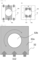
- a susceptor 32 having a triangular shape in side view is disposed inside the deposition chamber 31 .
- the pipe 102 is coupled to one wall of the deposition chamber 31 while the pipe 103 is coupled to the other wall of the deposition chamber 31.
- the gas mixture 112 is conveyed through the pipe 102 and supplied to the deposition chamber 31.
- the deposition chamber 31 is not particularly limited as long as it has sufficient stability against the raw material solution 21 to be used and a use temperature, and may be made of resin, metal, glass, ceramic, or a combination of these materials according to its purpose.
- the substrate 33 is capable of supporting a film to be formed.
- the substrate 33 has a circular shape in plan view, as can be inferred from the shape of the placement section illustrated in FIG. 2 .
- the shape is not limited thereto, and may be a rectangular or polygonal shape in plan view.
- the shape or size of the placement section 32b will be changed according to the shape or size of the substrate 33.
- a surface roughness (arithmetic mean roughness) Ra_sub of the surface of the substrate 33 is preferably equal to or less than the surface roughness (arithmetic mean roughness) Ra_cor of the surface of the smooth section 32a. This makes it possible to maintain the gas mixture as a laminar flow even on the substrate surface.
- the surface roughness (arithmetic mean roughness) Ra_sub of the surface of the substrate 33 is greater than the surface roughness (arithmetic mean roughness) Ra_cor of the surface of the smooth section 32a, abnormal growth is more likely to occur on the substrate 33.
- the surface roughness (arithmetic mean roughness) Ra_sub of the surface of the substrate 33 is preferably a value of 0.05 nm or more and 1 ⁇ m or less, for example.
- Such smoothness of the surface of the substrate 33 can easily be obtained, for example, in a case of sapphire, by lapping, with diamond abrasive grain, the surface of the substrate 33 obtained by processing crystal, and thereafter further giving a mirror finish by chemical mechanical polishing (CMP) using colloidal silica.
- CMP chemical mechanical polishing
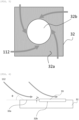
- the substrate 33 is placed on the substrate placement section 32b disposed in the susceptor 32, and a part of the gas mixture 112 flows along the smooth section 32a toward the substrate 33.
- an angle ⁇ between the inflow direction of the gas mixture 112 and the smooth section 32a is not particularly limited.
- the angle ⁇ is preferably 0° or more and 60° or less.
- the gas mixture 112 collides with the susceptor 32 or the upper surface of the substrate 33 to cause turbulence, which may partially cause generation of powder and adhesion thereof to the film surface.
- the angle ⁇ is 0° or more and 60° or less, such generation can be reduced.
- the angle ⁇ is more preferably 0° or more and 45° or less.
- angle ⁇ in the configuration of FIG. 1 can also be regarded as an inclination angle of the smooth section 32a with respect to the horizontal plane.
- Difference in height h between the surface of the substrate 33 and the surface of the smooth section 32a is not particularly limited, but preferably -1 mm or more and 1 mm or less. The difference in height h within such range leads to improved thickness uniformity at the edge of the substrate and no generation of turbulence at the edge. If there is a step of 1 mm or more, a film thickness distribution may occur, particularly near the edge of the substrate adjacent to the smooth section 32a.
- the positive or negative numerical value as described herein indicates the relative position of the substrate surface with respect to the surface of the smooth section.
- the negative value indicates that the substrate surface is recessed with respect to the surface of the smooth section, while the positive value indicates that the substrate surface is protruding with respect to the surface of the smooth section.
- the gas mixture concentrates at the edge of the substrate, resulting in a thicker film thickness.
- the step causes the flow of the gas mixture to pass over the edge of the substrate, resulting in a thinner film thickness. Additionally, such structure may cause turbulence in the flow of the gas mixture.
- the thickness of the film formed on the substrate can be measured by every known method. For example, ellipsometry, optical interference spectroscopy, a stylus method, a laser displacement method, or the like is suitably used.
- FIGs. 1 and 2 each illustrates the configuration in which the gas mixture 112 flows in one direction from the supply side to the exhaust side of the deposition chamber 31 relative to the substrate 33
- the present invention is not limited thereto and can be configured according to the supply method of the gas mixture 112 to the substrate.
- the method for forming a film according to the present invention includes a raw material mist forming step, a gas mixture forming step, a substrate placing step, a film forming step, and a discharge step.
- an entire surface refers to 80% or more of the total area of the substrate surface.
- an example of the film thickness distribution is a value obtained by using a known method such as optical interference spectroscopy to calculate film thickness at a plurality of points on the film surface, and dividing a difference between maximum and minimum values by a doubled average value.
- the foreign substance herein refers to a convex object on the film surface, particularly including both of a particle and an abnormally grown grain, and can be detected by a known wafer defect inspection apparatus.
- the film thus formed had clear and bright appearance in an area excluding 5 mm of an outer peripheral width of the film-formed surface.
- rocking curve of the ⁇ -Ga 2 O 3 (0006) plane was measured, and the half width was evaluated. Note that upon the rocking curve measurement, a four-crystal monochromator that combines two channel-cut crystals was used to increase monochromaticity of x-ray to enable the measurement with higher precision. Other measurement conditions are as follows.
Landscapes
- Chemical & Material Sciences (AREA)
- Engineering & Computer Science (AREA)
- Materials Engineering (AREA)
- Metallurgy (AREA)
- Organic Chemistry (AREA)
- General Chemical & Material Sciences (AREA)
- Chemical Kinetics & Catalysis (AREA)
- Mechanical Engineering (AREA)
- Crystallography & Structural Chemistry (AREA)
- Inorganic Chemistry (AREA)
- Dispersion Chemistry (AREA)
- Chemical Vapour Deposition (AREA)
Applications Claiming Priority (2)
| Application Number | Priority Date | Filing Date | Title |
|---|---|---|---|
| JP2022135279 | 2022-08-26 | ||
| PCT/JP2023/029452 WO2024043134A1 (ja) | 2022-08-26 | 2023-08-14 | 成膜方法、成膜装置、サセプター、及びα-酸化ガリウム膜 |
Publications (1)
| Publication Number | Publication Date |
|---|---|
| EP4579715A1 true EP4579715A1 (en) | 2025-07-02 |
Family
ID=90013193
Family Applications (1)
| Application Number | Title | Priority Date | Filing Date |
|---|---|---|---|
| EP23857247.3A Pending EP4579715A1 (en) | 2022-08-26 | 2023-08-14 | Film forming method, film forming device, susceptor, and a-gallium oxide film |
Country Status (7)
| Country | Link |
|---|---|
| US (1) | US20260055504A1 (https=) |
| EP (1) | EP4579715A1 (https=) |
| JP (1) | JPWO2024043134A1 (https=) |
| KR (1) | KR20250057789A (https=) |
| CN (1) | CN119768894A (https=) |
| TW (1) | TW202442926A (https=) |
| WO (1) | WO2024043134A1 (https=) |
Family Cites Families (16)
| Publication number | Priority date | Publication date | Assignee | Title |
|---|---|---|---|---|
| JP4909494B2 (ja) * | 2003-12-26 | 2012-04-04 | ルネサスエレクトロニクス株式会社 | 半導体製造装置および半導体装置の製造方法 |
| JP5793732B2 (ja) | 2011-07-27 | 2015-10-14 | 高知県公立大学法人 | ドーパントを添加した結晶性の高い導電性α型酸化ガリウム薄膜およびその生成方法 |
| JP6867637B2 (ja) | 2014-06-27 | 2021-04-28 | 株式会社Flosfia | サセプタ |
| WO2016051559A1 (ja) | 2014-10-01 | 2016-04-07 | 東芝三菱電機産業システム株式会社 | 成膜装置 |
| KR101765682B1 (ko) | 2014-11-03 | 2017-08-23 | 전북대학교산학협력단 | 신규 하이드로젠퍼옥사이드를 활성화하는 항산화 화합물 및 이를 이용한 약학 조성물 |
| JP6478103B2 (ja) | 2015-01-29 | 2019-03-06 | 株式会社Flosfia | 成膜装置および成膜方法 |
| JP7130962B2 (ja) * | 2018-01-11 | 2022-09-06 | 株式会社デンソー | 成膜方法及び成膜装置 |
| JP7105703B2 (ja) * | 2019-01-08 | 2022-07-25 | 信越化学工業株式会社 | 酸化物半導体膜、積層体及び酸化物半導体膜の製造方法 |
| JP7159449B2 (ja) * | 2019-03-28 | 2022-10-24 | 日本碍子株式会社 | 下地基板及びその製造方法 |
| JP6784871B1 (ja) * | 2019-04-24 | 2020-11-11 | 日本碍子株式会社 | 半導体膜 |
| JP7212890B2 (ja) * | 2019-06-05 | 2023-01-26 | 株式会社デンソー | 酸化物膜の成膜方法、半導体装置の製造方法、及び、酸化物膜の成膜装置 |
| JP7045014B2 (ja) * | 2019-08-28 | 2022-03-31 | 信越化学工業株式会社 | 積層構造体の製造方法 |
| JP7170617B2 (ja) * | 2019-10-24 | 2022-11-14 | 信越化学工業株式会社 | ガリウム前駆体の製造方法およびこれを用いた積層体の製造方法 |
| JP6994694B2 (ja) * | 2020-02-27 | 2022-01-14 | 信越化学工業株式会社 | 成膜用霧化装置及びこれを用いた成膜装置 |
| JP7737685B2 (ja) * | 2020-12-12 | 2025-09-11 | 高知県公立大学法人 | Ga2O3薄膜の製造方法 |
| TWM633935U (zh) * | 2021-04-07 | 2022-11-11 | 日商信越化學工業股份有限公司 | 積層體的製造系統、積層體以及半導體裝置 |
-
2023
- 2023-08-14 CN CN202380061363.3A patent/CN119768894A/zh active Pending
- 2023-08-14 WO PCT/JP2023/029452 patent/WO2024043134A1/ja not_active Ceased
- 2023-08-14 JP JP2024542763A patent/JPWO2024043134A1/ja active Pending
- 2023-08-14 KR KR1020257005527A patent/KR20250057789A/ko active Pending
- 2023-08-14 EP EP23857247.3A patent/EP4579715A1/en active Pending
- 2023-08-14 US US19/102,895 patent/US20260055504A1/en active Pending
- 2023-08-23 TW TW112131627A patent/TW202442926A/zh unknown
Also Published As
| Publication number | Publication date |
|---|---|
| KR20250057789A (ko) | 2025-04-29 |
| CN119768894A (zh) | 2025-04-04 |
| JPWO2024043134A1 (https=) | 2024-02-29 |
| WO2024043134A1 (ja) | 2024-02-29 |
| US20260055504A1 (en) | 2026-02-26 |
| TW202442926A (zh) | 2024-11-01 |
Similar Documents
| Publication | Publication Date | Title |
|---|---|---|
| JP7289357B2 (ja) | 半導体膜 | |
| EP1724817A1 (en) | Film forming apparatus | |
| CN113574214A (zh) | 基底基板及其制造方法 | |
| TW201940762A (zh) | Iii族氮化物單結晶製造裝置、使用該裝置之iii族氮化物單結晶之製造方法、及氮化鋁單結晶 | |
| JP7410159B2 (ja) | 半導体膜 | |
| EP4579715A1 (en) | Film forming method, film forming device, susceptor, and a-gallium oxide film | |
| JP6635756B2 (ja) | Iii族窒化物単結晶製造装置、該装置を用いたiii族窒化物単結晶の製造方法、及び窒化アルミニウム単結晶 | |
| TW201943882A (zh) | 氣相成長方法 | |
| EP4678785A1 (en) | Film formation nozzle and film formation device | |
| EP4517801A1 (en) | Film forming method, film forming apparatus, and multilayer body | |
| EP4321657A1 (en) | Method for manufacturing layered body, device for manufacturing layered body, layered body, and semiconductor device | |
| JP7775275B2 (ja) | 製膜方法、製膜装置及び積層体 | |
| EP4578990A1 (en) | Film deposition method, film deposition device, and alfa-ga2o3 film | |
| EP4539108A1 (en) | Film formation method and film formation device | |
| EP4428902A1 (en) | Film forming device, film forming method, oxide semiconductor film and multilayer body | |
| JP7591154B2 (ja) | 半導体膜及び複合基板 | |
| EP4661060A1 (en) | Nozzle cleaning method, film formation method for forming crystalline oxide film, and film formation device | |
| JP2025091752A (ja) | 成膜方法及び成膜装置 | |
| US20240410077A1 (en) | Method and apparatus for producing nitrogen compound |
Legal Events
| Date | Code | Title | Description |
|---|---|---|---|
| STAA | Information on the status of an ep patent application or granted ep patent |
Free format text: STATUS: THE INTERNATIONAL PUBLICATION HAS BEEN MADE |
|
| PUAI | Public reference made under article 153(3) epc to a published international application that has entered the european phase |
Free format text: ORIGINAL CODE: 0009012 |
|
| STAA | Information on the status of an ep patent application or granted ep patent |
Free format text: STATUS: REQUEST FOR EXAMINATION WAS MADE |
|
| 17P | Request for examination filed |
Effective date: 20250218 |
|
| AK | Designated contracting states |
Kind code of ref document: A1 Designated state(s): AL AT BE BG CH CY CZ DE DK EE ES FI FR GB GR HR HU IE IS IT LI LT LU LV MC ME MK MT NL NO PL PT RO RS SE SI SK SM TR |
|
| DAV | Request for validation of the european patent (deleted) | ||
| DAX | Request for extension of the european patent (deleted) |