EP4538414A2 - Verfahren zur substratverarbeitung, verfahren zur herstellung eines halbleiterbauelements, substratverarbeitungsvorrichtung und programm - Google Patents
Verfahren zur substratverarbeitung, verfahren zur herstellung eines halbleiterbauelements, substratverarbeitungsvorrichtung und programm Download PDFInfo
- Publication number
- EP4538414A2 EP4538414A2 EP25159603.7A EP25159603A EP4538414A2 EP 4538414 A2 EP4538414 A2 EP 4538414A2 EP 25159603 A EP25159603 A EP 25159603A EP 4538414 A2 EP4538414 A2 EP 4538414A2
- Authority
- EP
- European Patent Office
- Prior art keywords
- film
- substrate
- concave portion
- precursor
- hydroxyl group
- Prior art date
- Legal status (The legal status is an assumption and is not a legal conclusion. Google has not performed a legal analysis and makes no representation as to the accuracy of the status listed.)
- Pending
Links
Images







Classifications
-
- H—ELECTRICITY
- H10—SEMICONDUCTOR DEVICES; ELECTRIC SOLID-STATE DEVICES NOT OTHERWISE PROVIDED FOR
- H10P—GENERIC PROCESSES OR APPARATUS FOR THE MANUFACTURE OR TREATMENT OF DEVICES COVERED BY CLASS H10
- H10P14/00—Formation of materials, e.g. in the shape of layers or pillars
- H10P14/60—Formation of materials, e.g. in the shape of layers or pillars of insulating materials
- H10P14/66—Formation of materials, e.g. in the shape of layers or pillars of insulating materials characterised by the type of materials
- H10P14/668—Formation of materials, e.g. in the shape of layers or pillars of insulating materials characterised by the type of materials the materials being characterised by the deposition precursor materials
- H10P14/6681—Formation of materials, e.g. in the shape of layers or pillars of insulating materials characterised by the type of materials the materials being characterised by the deposition precursor materials the precursor containing a compound comprising Si
- H10P14/6682—Formation of materials, e.g. in the shape of layers or pillars of insulating materials characterised by the type of materials the materials being characterised by the deposition precursor materials the precursor containing a compound comprising Si the compound being a silane, e.g. disilane, methylsilane or chlorosilane
-
- H—ELECTRICITY
- H10—SEMICONDUCTOR DEVICES; ELECTRIC SOLID-STATE DEVICES NOT OTHERWISE PROVIDED FOR
- H10D—INORGANIC ELECTRIC SEMICONDUCTOR DEVICES
- H10D62/00—Semiconductor bodies, or regions thereof, of devices having potential barriers
- H10D62/10—Shapes, relative sizes or dispositions of the regions of the semiconductor bodies; Shapes of the semiconductor bodies
- H10D62/117—Shapes of semiconductor bodies
- H10D62/118—Nanostructure semiconductor bodies
-
- H—ELECTRICITY
- H10—SEMICONDUCTOR DEVICES; ELECTRIC SOLID-STATE DEVICES NOT OTHERWISE PROVIDED FOR
- H10P—GENERIC PROCESSES OR APPARATUS FOR THE MANUFACTURE OR TREATMENT OF DEVICES COVERED BY CLASS H10
- H10P14/00—Formation of materials, e.g. in the shape of layers or pillars
- H10P14/60—Formation of materials, e.g. in the shape of layers or pillars of insulating materials
- H10P14/65—Formation of materials, e.g. in the shape of layers or pillars of insulating materials characterised by treatments performed before or after the formation of the materials
- H10P14/6502—Formation of materials, e.g. in the shape of layers or pillars of insulating materials characterised by treatments performed before or after the formation of the materials of treatments performed before formation of the materials
-
- H—ELECTRICITY
- H10—SEMICONDUCTOR DEVICES; ELECTRIC SOLID-STATE DEVICES NOT OTHERWISE PROVIDED FOR
- H10P—GENERIC PROCESSES OR APPARATUS FOR THE MANUFACTURE OR TREATMENT OF DEVICES COVERED BY CLASS H10
- H10P14/00—Formation of materials, e.g. in the shape of layers or pillars
- H10P14/60—Formation of materials, e.g. in the shape of layers or pillars of insulating materials
- H10P14/69—Inorganic materials
- H10P14/692—Inorganic materials composed of oxides, glassy oxides or oxide-based glasses
- H10P14/6921—Inorganic materials composed of oxides, glassy oxides or oxide-based glasses containing silicon
- H10P14/6922—Inorganic materials composed of oxides, glassy oxides or oxide-based glasses containing silicon the material containing Si, O and at least one of H, N, C, F or other non-metal elements, e.g. SiOC, SiOC:H or SiONC
-
- C—CHEMISTRY; METALLURGY
- C23—COATING METALLIC MATERIAL; COATING MATERIAL WITH METALLIC MATERIAL; CHEMICAL SURFACE TREATMENT; DIFFUSION TREATMENT OF METALLIC MATERIAL; COATING BY VACUUM EVAPORATION, BY SPUTTERING, BY ION IMPLANTATION OR BY CHEMICAL VAPOUR DEPOSITION, IN GENERAL; INHIBITING CORROSION OF METALLIC MATERIAL OR INCRUSTATION IN GENERAL
- C23C—COATING METALLIC MATERIAL; COATING MATERIAL WITH METALLIC MATERIAL; SURFACE TREATMENT OF METALLIC MATERIAL BY DIFFUSION INTO THE SURFACE, BY CHEMICAL CONVERSION OR SUBSTITUTION; COATING BY VACUUM EVAPORATION, BY SPUTTERING, BY ION IMPLANTATION OR BY CHEMICAL VAPOUR DEPOSITION, IN GENERAL
- C23C16/00—Chemical coating by decomposition of gaseous compounds, without leaving reaction products of surface material in the coating, i.e. chemical vapour deposition [CVD] processes
- C23C16/02—Pretreatment of the material to be coated
- C23C16/0227—Pretreatment of the material to be coated by cleaning or etching
-
- C—CHEMISTRY; METALLURGY
- C23—COATING METALLIC MATERIAL; COATING MATERIAL WITH METALLIC MATERIAL; CHEMICAL SURFACE TREATMENT; DIFFUSION TREATMENT OF METALLIC MATERIAL; COATING BY VACUUM EVAPORATION, BY SPUTTERING, BY ION IMPLANTATION OR BY CHEMICAL VAPOUR DEPOSITION, IN GENERAL; INHIBITING CORROSION OF METALLIC MATERIAL OR INCRUSTATION IN GENERAL
- C23C—COATING METALLIC MATERIAL; COATING MATERIAL WITH METALLIC MATERIAL; SURFACE TREATMENT OF METALLIC MATERIAL BY DIFFUSION INTO THE SURFACE, BY CHEMICAL CONVERSION OR SUBSTITUTION; COATING BY VACUUM EVAPORATION, BY SPUTTERING, BY ION IMPLANTATION OR BY CHEMICAL VAPOUR DEPOSITION, IN GENERAL
- C23C16/00—Chemical coating by decomposition of gaseous compounds, without leaving reaction products of surface material in the coating, i.e. chemical vapour deposition [CVD] processes
- C23C16/02—Pretreatment of the material to be coated
- C23C16/0227—Pretreatment of the material to be coated by cleaning or etching
- C23C16/0236—Pretreatment of the material to be coated by cleaning or etching by etching with a reactive gas
-
- C—CHEMISTRY; METALLURGY
- C23—COATING METALLIC MATERIAL; COATING MATERIAL WITH METALLIC MATERIAL; CHEMICAL SURFACE TREATMENT; DIFFUSION TREATMENT OF METALLIC MATERIAL; COATING BY VACUUM EVAPORATION, BY SPUTTERING, BY ION IMPLANTATION OR BY CHEMICAL VAPOUR DEPOSITION, IN GENERAL; INHIBITING CORROSION OF METALLIC MATERIAL OR INCRUSTATION IN GENERAL
- C23C—COATING METALLIC MATERIAL; COATING MATERIAL WITH METALLIC MATERIAL; SURFACE TREATMENT OF METALLIC MATERIAL BY DIFFUSION INTO THE SURFACE, BY CHEMICAL CONVERSION OR SUBSTITUTION; COATING BY VACUUM EVAPORATION, BY SPUTTERING, BY ION IMPLANTATION OR BY CHEMICAL VAPOUR DEPOSITION, IN GENERAL
- C23C16/00—Chemical coating by decomposition of gaseous compounds, without leaving reaction products of surface material in the coating, i.e. chemical vapour deposition [CVD] processes
- C23C16/04—Coating on selected surface areas, e.g. using masks
-
- C—CHEMISTRY; METALLURGY
- C23—COATING METALLIC MATERIAL; COATING MATERIAL WITH METALLIC MATERIAL; CHEMICAL SURFACE TREATMENT; DIFFUSION TREATMENT OF METALLIC MATERIAL; COATING BY VACUUM EVAPORATION, BY SPUTTERING, BY ION IMPLANTATION OR BY CHEMICAL VAPOUR DEPOSITION, IN GENERAL; INHIBITING CORROSION OF METALLIC MATERIAL OR INCRUSTATION IN GENERAL
- C23C—COATING METALLIC MATERIAL; COATING MATERIAL WITH METALLIC MATERIAL; SURFACE TREATMENT OF METALLIC MATERIAL BY DIFFUSION INTO THE SURFACE, BY CHEMICAL CONVERSION OR SUBSTITUTION; COATING BY VACUUM EVAPORATION, BY SPUTTERING, BY ION IMPLANTATION OR BY CHEMICAL VAPOUR DEPOSITION, IN GENERAL
- C23C16/00—Chemical coating by decomposition of gaseous compounds, without leaving reaction products of surface material in the coating, i.e. chemical vapour deposition [CVD] processes
- C23C16/04—Coating on selected surface areas, e.g. using masks
- C23C16/045—Coating cavities or hollow spaces, e.g. interior of tubes; Infiltration of porous substrates
-
- C—CHEMISTRY; METALLURGY
- C23—COATING METALLIC MATERIAL; COATING MATERIAL WITH METALLIC MATERIAL; CHEMICAL SURFACE TREATMENT; DIFFUSION TREATMENT OF METALLIC MATERIAL; COATING BY VACUUM EVAPORATION, BY SPUTTERING, BY ION IMPLANTATION OR BY CHEMICAL VAPOUR DEPOSITION, IN GENERAL; INHIBITING CORROSION OF METALLIC MATERIAL OR INCRUSTATION IN GENERAL
- C23C—COATING METALLIC MATERIAL; COATING MATERIAL WITH METALLIC MATERIAL; SURFACE TREATMENT OF METALLIC MATERIAL BY DIFFUSION INTO THE SURFACE, BY CHEMICAL CONVERSION OR SUBSTITUTION; COATING BY VACUUM EVAPORATION, BY SPUTTERING, BY ION IMPLANTATION OR BY CHEMICAL VAPOUR DEPOSITION, IN GENERAL
- C23C16/00—Chemical coating by decomposition of gaseous compounds, without leaving reaction products of surface material in the coating, i.e. chemical vapour deposition [CVD] processes
- C23C16/22—Chemical coating by decomposition of gaseous compounds, without leaving reaction products of surface material in the coating, i.e. chemical vapour deposition [CVD] processes characterised by the deposition of inorganic material, other than metallic material
- C23C16/30—Deposition of compounds, mixtures or solid solutions, e.g. borides, carbides, nitrides
-
- C—CHEMISTRY; METALLURGY
- C23—COATING METALLIC MATERIAL; COATING MATERIAL WITH METALLIC MATERIAL; CHEMICAL SURFACE TREATMENT; DIFFUSION TREATMENT OF METALLIC MATERIAL; COATING BY VACUUM EVAPORATION, BY SPUTTERING, BY ION IMPLANTATION OR BY CHEMICAL VAPOUR DEPOSITION, IN GENERAL; INHIBITING CORROSION OF METALLIC MATERIAL OR INCRUSTATION IN GENERAL
- C23C—COATING METALLIC MATERIAL; COATING MATERIAL WITH METALLIC MATERIAL; SURFACE TREATMENT OF METALLIC MATERIAL BY DIFFUSION INTO THE SURFACE, BY CHEMICAL CONVERSION OR SUBSTITUTION; COATING BY VACUUM EVAPORATION, BY SPUTTERING, BY ION IMPLANTATION OR BY CHEMICAL VAPOUR DEPOSITION, IN GENERAL
- C23C16/00—Chemical coating by decomposition of gaseous compounds, without leaving reaction products of surface material in the coating, i.e. chemical vapour deposition [CVD] processes
- C23C16/44—Chemical coating by decomposition of gaseous compounds, without leaving reaction products of surface material in the coating, i.e. chemical vapour deposition [CVD] processes characterised by the method of coating
- C23C16/455—Chemical coating by decomposition of gaseous compounds, without leaving reaction products of surface material in the coating, i.e. chemical vapour deposition [CVD] processes characterised by the method of coating characterised by the method used for introducing gases into reaction chamber or for modifying gas flows in reaction chamber
- C23C16/45523—Pulsed gas flow or change of composition over time
- C23C16/45525—Atomic layer deposition [ALD]
- C23C16/45527—Atomic layer deposition [ALD] characterized by the ALD cycle, e.g. different flows or temperatures during half-reactions, unusual pulsing sequence, use of precursor mixtures or auxiliary reactants or activations
- C23C16/45534—Use of auxiliary reactants other than used for contributing to the composition of the main film, e.g. catalysts, activators or scavengers
-
- C—CHEMISTRY; METALLURGY
- C23—COATING METALLIC MATERIAL; COATING MATERIAL WITH METALLIC MATERIAL; CHEMICAL SURFACE TREATMENT; DIFFUSION TREATMENT OF METALLIC MATERIAL; COATING BY VACUUM EVAPORATION, BY SPUTTERING, BY ION IMPLANTATION OR BY CHEMICAL VAPOUR DEPOSITION, IN GENERAL; INHIBITING CORROSION OF METALLIC MATERIAL OR INCRUSTATION IN GENERAL
- C23C—COATING METALLIC MATERIAL; COATING MATERIAL WITH METALLIC MATERIAL; SURFACE TREATMENT OF METALLIC MATERIAL BY DIFFUSION INTO THE SURFACE, BY CHEMICAL CONVERSION OR SUBSTITUTION; COATING BY VACUUM EVAPORATION, BY SPUTTERING, BY ION IMPLANTATION OR BY CHEMICAL VAPOUR DEPOSITION, IN GENERAL
- C23C16/00—Chemical coating by decomposition of gaseous compounds, without leaving reaction products of surface material in the coating, i.e. chemical vapour deposition [CVD] processes
- C23C16/44—Chemical coating by decomposition of gaseous compounds, without leaving reaction products of surface material in the coating, i.e. chemical vapour deposition [CVD] processes characterised by the method of coating
- C23C16/46—Chemical coating by decomposition of gaseous compounds, without leaving reaction products of surface material in the coating, i.e. chemical vapour deposition [CVD] processes characterised by the method of coating characterised by the method used for heating the substrate
-
- H—ELECTRICITY
- H10—SEMICONDUCTOR DEVICES; ELECTRIC SOLID-STATE DEVICES NOT OTHERWISE PROVIDED FOR
- H10P—GENERIC PROCESSES OR APPARATUS FOR THE MANUFACTURE OR TREATMENT OF DEVICES COVERED BY CLASS H10
- H10P14/00—Formation of materials, e.g. in the shape of layers or pillars
- H10P14/60—Formation of materials, e.g. in the shape of layers or pillars of insulating materials
-
- H—ELECTRICITY
- H10—SEMICONDUCTOR DEVICES; ELECTRIC SOLID-STATE DEVICES NOT OTHERWISE PROVIDED FOR
- H10P—GENERIC PROCESSES OR APPARATUS FOR THE MANUFACTURE OR TREATMENT OF DEVICES COVERED BY CLASS H10
- H10P14/00—Formation of materials, e.g. in the shape of layers or pillars
- H10P14/60—Formation of materials, e.g. in the shape of layers or pillars of insulating materials
- H10P14/61—Formation of materials, e.g. in the shape of layers or pillars of insulating materials using masks
-
- H—ELECTRICITY
- H10—SEMICONDUCTOR DEVICES; ELECTRIC SOLID-STATE DEVICES NOT OTHERWISE PROVIDED FOR
- H10P—GENERIC PROCESSES OR APPARATUS FOR THE MANUFACTURE OR TREATMENT OF DEVICES COVERED BY CLASS H10
- H10P14/00—Formation of materials, e.g. in the shape of layers or pillars
- H10P14/60—Formation of materials, e.g. in the shape of layers or pillars of insulating materials
- H10P14/63—Formation of materials, e.g. in the shape of layers or pillars of insulating materials characterised by the formation processes
- H10P14/6326—Deposition processes
- H10P14/6328—Deposition from the gas or vapour phase
- H10P14/6334—Deposition from the gas or vapour phase using decomposition or reaction of gaseous or vapour phase compounds, i.e. chemical vapour deposition
- H10P14/6338—Deposition from the gas or vapour phase using decomposition or reaction of gaseous or vapour phase compounds, i.e. chemical vapour deposition the reactions being activated by other means than plasma or thermal, e.g. photo-CVD
-
- H—ELECTRICITY
- H10—SEMICONDUCTOR DEVICES; ELECTRIC SOLID-STATE DEVICES NOT OTHERWISE PROVIDED FOR
- H10P—GENERIC PROCESSES OR APPARATUS FOR THE MANUFACTURE OR TREATMENT OF DEVICES COVERED BY CLASS H10
- H10P14/00—Formation of materials, e.g. in the shape of layers or pillars
- H10P14/60—Formation of materials, e.g. in the shape of layers or pillars of insulating materials
- H10P14/63—Formation of materials, e.g. in the shape of layers or pillars of insulating materials characterised by the formation processes
- H10P14/6326—Deposition processes
- H10P14/6328—Deposition from the gas or vapour phase
- H10P14/6334—Deposition from the gas or vapour phase using decomposition or reaction of gaseous or vapour phase compounds, i.e. chemical vapour deposition
- H10P14/6339—Deposition from the gas or vapour phase using decomposition or reaction of gaseous or vapour phase compounds, i.e. chemical vapour deposition deposition by cyclic CVD, e.g. ALD, ALE or pulsed CVD
-
- H—ELECTRICITY
- H10—SEMICONDUCTOR DEVICES; ELECTRIC SOLID-STATE DEVICES NOT OTHERWISE PROVIDED FOR
- H10P—GENERIC PROCESSES OR APPARATUS FOR THE MANUFACTURE OR TREATMENT OF DEVICES COVERED BY CLASS H10
- H10P14/00—Formation of materials, e.g. in the shape of layers or pillars
- H10P14/60—Formation of materials, e.g. in the shape of layers or pillars of insulating materials
- H10P14/65—Formation of materials, e.g. in the shape of layers or pillars of insulating materials characterised by treatments performed before or after the formation of the materials
- H10P14/6502—Formation of materials, e.g. in the shape of layers or pillars of insulating materials characterised by treatments performed before or after the formation of the materials of treatments performed before formation of the materials
- H10P14/6504—In-situ cleaning
-
- H—ELECTRICITY
- H10—SEMICONDUCTOR DEVICES; ELECTRIC SOLID-STATE DEVICES NOT OTHERWISE PROVIDED FOR
- H10P—GENERIC PROCESSES OR APPARATUS FOR THE MANUFACTURE OR TREATMENT OF DEVICES COVERED BY CLASS H10
- H10P14/00—Formation of materials, e.g. in the shape of layers or pillars
- H10P14/60—Formation of materials, e.g. in the shape of layers or pillars of insulating materials
- H10P14/66—Formation of materials, e.g. in the shape of layers or pillars of insulating materials characterised by the type of materials
- H10P14/668—Formation of materials, e.g. in the shape of layers or pillars of insulating materials characterised by the type of materials the materials being characterised by the deposition precursor materials
- H10P14/6681—Formation of materials, e.g. in the shape of layers or pillars of insulating materials characterised by the type of materials the materials being characterised by the deposition precursor materials the precursor containing a compound comprising Si
- H10P14/6687—Formation of materials, e.g. in the shape of layers or pillars of insulating materials characterised by the type of materials the materials being characterised by the deposition precursor materials the precursor containing a compound comprising Si the compound comprising silicon and nitrogen
-
- H—ELECTRICITY
- H10—SEMICONDUCTOR DEVICES; ELECTRIC SOLID-STATE DEVICES NOT OTHERWISE PROVIDED FOR
- H10P—GENERIC PROCESSES OR APPARATUS FOR THE MANUFACTURE OR TREATMENT OF DEVICES COVERED BY CLASS H10
- H10P72/00—Handling or holding of wafers, substrates or devices during manufacture or treatment thereof
- H10P72/04—Apparatus for manufacture or treatment
- H10P72/0431—Apparatus for thermal treatment
-
- H—ELECTRICITY
- H10—SEMICONDUCTOR DEVICES; ELECTRIC SOLID-STATE DEVICES NOT OTHERWISE PROVIDED FOR
- H10P—GENERIC PROCESSES OR APPARATUS FOR THE MANUFACTURE OR TREATMENT OF DEVICES COVERED BY CLASS H10
- H10P14/00—Formation of materials, e.g. in the shape of layers or pillars
- H10P14/60—Formation of materials, e.g. in the shape of layers or pillars of insulating materials
- H10P14/63—Formation of materials, e.g. in the shape of layers or pillars of insulating materials characterised by the formation processes
- H10P14/6302—Non-deposition formation processes
- H10P14/6304—Formation by oxidation, e.g. oxidation of the substrate
- H10P14/6306—Formation by oxidation, e.g. oxidation of the substrate of the semiconductor materials
- H10P14/6308—Formation by oxidation, e.g. oxidation of the substrate of the semiconductor materials of Group IV semiconductors
- H10P14/6309—Formation by oxidation, e.g. oxidation of the substrate of the semiconductor materials of Group IV semiconductors of silicon in uncombined form, i.e. pure silicon
-
- H—ELECTRICITY
- H10—SEMICONDUCTOR DEVICES; ELECTRIC SOLID-STATE DEVICES NOT OTHERWISE PROVIDED FOR
- H10P—GENERIC PROCESSES OR APPARATUS FOR THE MANUFACTURE OR TREATMENT OF DEVICES COVERED BY CLASS H10
- H10P14/00—Formation of materials, e.g. in the shape of layers or pillars
- H10P14/60—Formation of materials, e.g. in the shape of layers or pillars of insulating materials
- H10P14/63—Formation of materials, e.g. in the shape of layers or pillars of insulating materials characterised by the formation processes
- H10P14/6302—Non-deposition formation processes
- H10P14/6322—Formation by thermal treatments
Definitions
- the present disclosure relates to a method of processing a substrate, a method of manufacturing a semiconductor device, a substrate processing apparatus, and a program.
- a technique that includes: (a) forming a film formation suppression layer on a surface, which is composed of a first material, of a concave portion of the substrate, by supplying a precursor to the substrate provided with the concave portion on a surface of the substrate to adsorb at least a portion of a molecular structure of molecules constituting the precursor on the surface of the first material of the concave portion, the concave portion having a top surface and a side surface composed of the first material containing a first element and a bottom surface composed of a second material containing a second element; and (b) growing a film on a surface of the second material of the concave portion by supplying a film-forming material to the substrate having the film formation suppression layer formed on the surface of the first material.
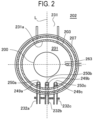
- FIGS. 1 to 4 and 5A to 5D One embodiment of the present disclosure will now be described mainly with reference to FIGS. 1 to 4 and 5A to 5D .
- the drawings used in the following description are all schematic, and the dimensional relationship, ratios, and the like of various elements shown in figures do not always match the actual ones. Further, the dimensional relationship, ratios, and the like of various elements between plural figures do not always match each other.
- a process furnace 202 includes a heater 207 as a temperature adjustor (a heating part).
- the heater 207 has a cylindrical shape and is supported by a support plate so as to be vertically installed.
- the heater 207 also functions as an activation mechanism (an excitation part) configured to thermally activate (excite) a gas.
- a reaction tube 203 is disposed inside the heater 207 to be concentric with the heater 207.
- the reaction tube 203 is made of, for example, a heat resistant material such as quartz (SiO 2 ) or silicon carbide (SiC), and has a cylindrical shape with its upper end closed and its lower end opened.
- a manifold 209 is disposed to be concentric with the reaction tube 203 under the reaction tube 203.
- the manifold 209 is made of, for example, a metal material such as stainless steel (SUS), and has a cylindrical shape with both of its upper and lower ends opened. The upper end portion of the manifold 209 engages with the lower end portion of the reaction tube 203 so as to support the reaction tube 203.
- a process container (reaction container) mainly includes the reaction tube 203 and the manifold 209.
- a process chamber 201 is formed in a hollow cylindrical portion of the process container. The process chamber 201 is configured to accommodate a plurality of wafers 200 as substrates. Processing on the wafers 200 is performed in the process chamber 201.
- Nozzles 249a to 249c as first to third supply parts are provided in the process chamber 201 so as to penetrate through a sidewall of the manifold 209.
- the nozzles 249a to 249c are also referred to as first to third nozzles, respectively.
- the nozzles 249a to 249c are made of, for example, a heat resistant material such as quartz or SiC.
- Gas supply pipes 232a to 232c are connected to the nozzles 249a to 249c, respectively.
- the nozzles 249a to 249c are different nozzles, and each of the nozzles 249a and 249c is provided adjacent to the nozzle 249b.
- Mass flow controllers (MFCs) 241a to 241c which are flow rate controllers (flow rate control parts), and valves 243a to 243c, which are opening/closing valves, are provided in the gas supply pipes 232a to 232c, respectively, sequentially from the upstream side of a gas flow.
- Each of gas supply pipes 232d and 232f is connected to the gas supply pipe 232a at the downstream side of the valves 243a.
- Each of gas supply pipes 232e and 232g is connected to the gas supply pipe 232b at the downstream side of the valves 243b.
- a gas supply pipe 232h is connected to the gas supply pipe 232c at the downstream side of the valves 243c.
- MFCs 241d to 241h and valves 243d to 243h are provided in the gas supply pipes 232d to 232h, respectively, sequentially from the upstream side of a gas flow.
- the gas supply pipes 232a to 232h are made of, for example, a metal material such as SUS.
- each of the nozzles 249a to 249c is provided in an annular space (in a plan view) between an inner wall of the reaction tube 203 and the wafers 200 so as to extend upward from a lower portion of the inner wall of the reaction tube 203 to an upper portion thereof, that is, along an arrangement direction of the wafers 200.
- each of the nozzles 249a to 249c is provided in a region horizontally surrounding a wafer arrangement region in which the wafers 200 are arranged at a lateral side of the wafer arrangement region, along the wafer arrangement region.
- the nozzle 249b is disposed so as to face an exhaust port 231a to be described later in a straight line with the centers of the wafers 200 loaded into the process chamber 201, which are interposed therebetween.
- the nozzles 249a and 249c are arranged so as to sandwich a straight line L passing through the nozzle 249b and the center of the exhaust port 231a from both sides along the inner wall of the reaction tube 203 (the outer peripheral portion of the wafers 200).
- the straight line L is also a straight line passing through the nozzle 249b and the centers of the wafers 200. That is, it can be said that the nozzle 249c is provided on the side opposite to the nozzle 249a with the straight line L interposed therebetween.
- the nozzles 249a and 249c are arranged in line symmetry with the straight line L as the axis of symmetry.
- Gas supply holes 250a to 250c for supplying a gas are formed on the side surfaces of the nozzles 249a to 249c, respectively.
- Each of the gas supply holes 250a to 250c is opened so as to oppose (face) the exhaust port 231a in a plan view, which enables a gas to be supplied toward the wafers 200.
- a plurality of gas supply holes 250a to 250c are formed from the lower portion of the reaction tube 203 to the upper portion thereof.
- a precursor (precursor gas) is supplied from the gas supply pipe 232a into the process chamber 201 via the MFC 241a, the valve 243a, and the nozzle 249a.
- a raw material which is one of film-forming materials (film-forming gases), is supplied from the gas supply pipe 232b into the process chamber 201 via the MFC 241b, the valve 243b, and the nozzle 249b.
- a reactant which is one of film-forming materials (film-forming gases) and is also one of reaction materials, is supplied from the gas supply pipe 232c into the process chamber 201 via the MFC 241c, the valve 243c, and the nozzle 249c.
- a catalyst which is one of film-forming materials (film-forming gases) and is also one of reaction materials, is supplied from the gas supply pipe 232d into the process chamber 201 via the MFC 241d, the valve 243d, the gas supply pipe 232a, and the nozzle 249a.
- An inert gas is supplied from the gas supply pipes 232f to 232h into the process chamber 201 via the MFCs 241f to 241h, the valves 243f to 243h, the gas supply pipes 232a to 232c, and the nozzles 249a to 249c, respectively.
- the inert gas acts as a purge gas, a carrier gas, a dilution gas, or the like.
- a precursor supply system mainly includes the gas supply pipe 232a, the MFC 241a, and the valve 243a.
- a raw material supply system mainly includes the gas supply pipe 232b, the MFC 241b, and the valve 243b.
- a reactant supply system mainly includes the gas supply pipe 232c, the MFC 241c, and the valve 243c.
- a catalyst supply system mainly includes the gas supply pipe 232d, the MFC 241d, and the valve 243d.
- An etchant supply system mainly includes the gas supply pipe 232e, the MFC 241e, and the valve 243e.
- An inert gas supply system mainly includes the gas supply pipes 232f to 232h, the MFCs 241f to 241h, and the valves 243f to 243h.
- Each or both of the raw material supply system and the reactant supply system are also referred to as a film-forming material supply system.
- Each or all of the raw material supply system, the reactant supply system, and the catalyst supply system are also referred to as a film-forming material supply system.
- Each or both of the reactant supply system and the catalyst supply system are also referred to as a reaction material supply system.
- One or all of the above-described various supply systems may be configured as an integrated-type supply system 248 in which the valves 243a to 243h, the MFCs 241a to 241h, and so on are integrated.
- the integrated-type supply system 248 is connected to each of the gas supply pipes 232a to 232h.
- the integrated-type supply system 248 is configured such that operations of supplying various materials (various gases) into the gas supply pipes 232a to 232h (that is, the opening/closing operation of the valves 243a to 243h, the flow rate adjustment operation by the MFCs 241a to 241h, and the like) are controlled by a controller 121 which will be described later.
- the integrated-type supply system 248 is configured as an integral type or detachable-type integrated unit, and may be attached to and detached from the gas supply pipes 232a to 232h and the like on an integrated unit basis, so that the maintenance, replacement, extension, etc. of the integrated-type supply system 248 can be performed on an integrated unit basis.
- the exhaust port 23 1a for exhausting an internal atmosphere of the process chamber 201 is provided below a sidewall of the reaction tube 203.
- the exhaust port 231a is provided at a position opposing (facing) the nozzles 249a to 249c (the gas supply holes 250a to 250c) with the wafers 200 interposed therebetween.
- the exhaust port 231a may be provided from a lower portion of the sidewall of the reaction tube 203 to an upper portion thereof, that is, along the wafer arrangement region.
- An exhaust pipe 231 is connected to the exhaust port 231a.
- a vacuum exhaust device for example, a vacuum pump 246, is connected to the exhaust pipe 231 via a pressure sensor 245, which is a pressure detector (pressure detection part) for detecting the internal pressure of the process chamber 201, and an auto pressure controller (APC) valve 244, which is a pressure regulator (pressure adjustment part).
- the APC valve 244 is configured to perform or stop a vacuum exhausting operation in the process chamber 201 by opening/closing the valve while the vacuum pump 246 is actuated, and is also configured to adjust the internal pressure of the process chamber 201 by adjusting an opening degree of the valve based on pressure information detected by the pressure sensor 245 while the vacuum pump 246 is actuated.
- An exhaust system mainly includes the exhaust pipe 231, the APC valve 244, and the pressure sensor 245.
- the exhaust system may include the vacuum pump 246.
- a seal cap 219 which serves as a furnace opening cover configured to hermetically seal a lower end opening of the manifold 209, is provided under the manifold 209.
- the seal cap 219 is made of, for example, a metal material such as SUS, and is formed in a disc shape.
- An O-ring 220b which is a seal making contact with the lower end of the manifold 209, is provided on an upper surface of the seal cap 219.
- a rotation mechanism 267 configured to rotate a boat 217, which will be described later, is installed under the seal cap 219.
- a rotary shaft 255 of the rotation mechanism 267 is connected to the boat 217 through the seal cap 219.
- the rotation mechanism 267 is configured to rotate the wafers 200 by rotating the boat 217.
- the seal cap 219 is configured to be vertically moved up and down by a boat elevator 115 which is an elevating mechanism installed outside the reaction tube 203.
- the boat elevator 115 is configured as a transfer device (transfer mechanism) which loads/unloads (transfers) the wafers 200 into/out of the process chamber 201 by moving the seal cap 219 up and down.
- a shutter 219s which serves as a furnace opening cover configured to hermetically seal a lower end opening of the manifold 209 in a state where the seal cap 219 is lowered and the boat 217 is unloaded from the process chamber 201, is provided under the manifold 209.
- the shutter 219s is made of, for example, a metal material such as SUS, and is formed in a disc shape.
- An O-ring 220c which is a seal making contact with the lower end of the manifold 209, is provided on an upper surface of the shutter 219s.
- the opening/closing operation (such as elevation operation, rotation operation, or the like) of the shutter 219s is controlled by a shutter opening/closing mechanism 115s.
- the boat 217 serving as a substrate support is configured to support a plurality of wafers 200, for example, 25 to 200 wafers, in such a state that the wafers 200 are arranged in a horizontal posture and in multiple stages along a vertical direction with the centers of the wafers 200 aligned with one another. That is, the boat 217 is configured to arrange the wafers 200 to be spaced apart from each other.
- the boat 217 is made of a heat resistant material such as quartz or SiC.
- Heat insulating plates 218 made of a heat resistant material such as quartz or SiC are installed below the boat 217 in multiple stages.
- a temperature sensor 263 serving as a temperature detector is installed in the reaction tube 203. Based on temperature information detected by the temperature sensor 263, a state of supplying electric power to the heater 207 is adjusted such that an interior of the process chamber 201 has a desired temperature distribution.
- the temperature sensor 263 is provided along the inner wall of the reaction tube 203.
- a controller 121 which is a control part (control means), is configured as a computer including a central processing unit (CPU) 121a, a random access memory (RAM) 121b, a memory 121c, and an I/O port 121d.
- the RAM 121b, the memory 121c, and the I/O port 121d are configured to be capable of exchanging data with the CPU 121a via an internal bus 121e.
- An input/output device 122 formed of, e.g., a touch panel or the like, is connected to the controller 121. Further, an external memory 123 can be connected to the controller 121.
- the memory 121c is configured by, for example, a flash memory, a hard disk drive (HDD), or the like.
- a control program for controlling operations of a substrate processing apparatus, a process recipe in which sequences and conditions of substrate processing to be described later are written, etc. are readably stored in the memory 121c.
- the process recipe functions as a program for causing the controller 121 to execute each sequence in the substrate processing, which will be described later, to obtain an expected result.
- the process recipe and the control program may be generally and simply referred to as a "program.” Furthermore, the process recipe may be simply referred to as a "recipe.”
- program When the term “program” is used herein, it may indicate a case of including the recipe only, a case of including the control program only, or a case of including both the recipe and the control program.
- the RAM 121b is configured as a memory area (work area) in which programs or data read by the CPU 121a are temporarily stored.
- the CPU 121a is configured to read and execute the control program from the memory 121c.
- the CPU 121a is also configured to read the recipe from the memory 121c according to an input of an operation command from the input/output device 122.
- the CPU 121a is configured to control the flow rate adjusting operation of various kinds of materials (gases) by the MFCs 241a to 241h, the opening/closing operation of the valves 243a to 243h, the opening/closing operation of the APC valve 244, the pressure adjusting operation performed by the APC valve 244 based on the pressure sensor 245, the actuating and stopping operation of the vacuum pump 246, the temperature adjusting operation performed by the heater 207 based on the temperature sensor 263, the operation of rotating the boat 217 with the rotation mechanism 267 and adjusting the rotation speed of the boat 217, the operation of moving the boat 217 up and down by the boat elevator 115, the opening/closing operation of the shutter 219s by the shutter opening/closing mechanism 115s
- the controller 121 may be configured by installing, on the computer, the aforementioned program stored in the external memory 123.
- the external memory 123 may include a magnetic disk such as a HDD, an optical disc such as a CD, a magneto-optical disc such as a MO, a semiconductor memory such as a USB memory or a SSD, and the like.
- the memory 121c or the external memory 123 is configured as a non-transitory computer-readable recording medium.
- the memory 121c and the external memory 123 may be generally and simply referred to as a "recording medium.”
- the term “recording medium” may indicate a case of including the memory 121c only, a case of including the external memory 123 only, or a case of including both the memory 121c and the external memory 123.
- the program may be provided to the computer using communication means such as the Internet or a dedicated line, instead of using the external memory 123.
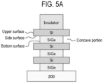
- a processing sequence example of forming a film in an inside of a concave portion formed on a surface of a wafer 200 as a substrate so as to bury the inside of the concave portion will be described mainly with reference to FIGS. 4 and 5A to 5D .
- the operations of the respective parts constituting the substrate processing apparatus are controlled by the controller 121.
- the concave portion having its upper surface and side surface composed of a first material containing a first element and its bottom surface composed of a second element different from the first element, whose depth direction is a direction (horizontal direction) parallel to the surface of the wafer 200, is provided on the surface of the wafer 200.
- FIG. 5A shows an example where the first element is silicon (Si), the second element is germanium (Ge), the first material is silicon (Si), and the second material is silicon germanium (SiGe). That is, in this example, the second material contains the second element in addition to the first element.
- the wafer 200 is made of single crystal Si. That is, the wafer 200 contains the first element.
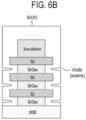
- a stacked structure in which the second material (SiGe) and the first material (Si) are alternately stacked is provided on the surface of the wafer 200, and an insulating film (insulator) is provided on the stacked structure. That is, a stacked structure in which the silicon germanium (SiGe) film and the silicon (Si) film are alternately stacked is provided on the surface of the wafer 200, and the insulating film (insulator) is provided on the stacked structure.
- the concave portion By partially removing a portion of a sidewall of the stacked structure of the SiGe film and the Si film, which is composed of the SiGe film, which is composed of the SiGe film, the concave portion having its upper surface and side surface composed of the first material (Si) and its bottom surface composed of the second material (SiGe), whose depth direction is a direction (horizontal direction) parallel to the surface of the wafer 200, is provided on the sidewall of the stacked structure.
- the concave portion having its upper surface and side surface composed of the first material (Si) and its bottom surface composed of the second material (SiGe), whose depth direction is a direction (horizontal direction) parallel to the surface of the wafer 200, is provided on the sidewall of the stacked structure.
- a portion of the concave portion composed of the second material (SiGe) is referred to as a bottom surface
- a portion of the concave portion composed of the first material (Si), which is in contact with the bottom surface and is provided perpendicular to the bottom surface is referred to as a side surface with respect to the bottom surface
- a portion of the concave portion composed of the first material (Si), which is not in contact with the bottom surface and is provided parallel to the bottom surface is referred to as a top surface with respect to the bottom surface.
- a processing sequence shown in FIG. 4 includes:
- step B includes: performing a cycle a predetermined number of times, the cycle including non-simultaneously performing:
- the film is grown starting from the bottom surface of the concave portion, the film is grown bottom-up in the concave portion, and the inside of the concave portion is buried by the film.
- a catalyst may be further supplied to the wafer 200.
- FIG. 4 shows an example in which the catalyst is further supplied as the film-forming material to the wafer 200 in each of step B1 and step B2.
- processing sequence shown in FIG. 4 further includes: step C of forming a hydroxyl group termination on the surface of the first material before performing step A, by supplying an oxidant as a reaction material to the wafer 200 to oxidize the surface of the first material. At this time, a hydroxyl group termination is formed on the surface of the second material as the surface of the second material is oxidized.
- the processing sequence shown in FIG. 4 further includes: step D of removing the hydroxyl group termination formed on the surface of the second material after performing step C and before performing step A, by heating an annealing (hereinafter, also referred to as ANL) the wafer 200 to sublimate an oxide formed on the surface of the second material. At this time, the hydroxyl group termination formed on the surface of the second material is removed while retaining the hydroxyl group termination formed on the surface of the first material.
- step D of removing the hydroxyl group termination formed on the surface of the second material after performing step C and before performing step A, by heating an annealing (hereinafter, also referred to as ANL) the wafer 200 to sublimate an oxide formed on the surface of the second material.
- ANL annealing
- the hydroxyl group termination is formed on the surface of the first material before performing step A, and the hydroxyl group termination is not formed on the surface of the second material before performing step A or a much smaller amount of hydroxyl group termination is formed on the surface of the second material than the amount of hydroxyl group termination on the surface of the first material.
- the hydroxyl group termination is also referred to as an OH termination.
- processing sequence shown in FIG. 4 further includes: step E of removing a native oxide film on the surfaces of the first material and the second material before performing step C, by supplying an etchant to the wafer 200.
- processing sequence shown in FIG. 4 further includes: step F of performing post-treatment (PT) on the film formed so as to bury the inside of the concave portion after performing step B, by heating and heat-treating the wafer 200.
- PT post-treatment
- the first element is Si
- the second element is Ge
- the first material is Si
- the second material is SiGe
- step B as a film, a silicon oxycarbide film (SiOC film), which is one of films containing oxygen (O) and carbon (C), or a silicon oxide film (SiOC film), which is one of films containing silicon (Si) and oxygen (O), is grown
- SiOC film silicon oxycarbide film
- SiOC film silicon oxide film
- wafer When the term “wafer” is used in the present disclosure, it may refer to “a wafer itself” or “a wafer and a stacked body of certain layers or films formed on a surface of the wafer.” When the phrase “a surface of a wafer” is used in the present disclosure, it may refer to "a surface of a wafer itself” or “a surface of a certain layer formed on a wafer.” When the expression “a certain layer is formed on a wafer” is used in the present disclosure, it may mean that "a certain layer is formed directly on a surface of a wafer itself” or that "a certain layer is formed on a layer formed on a wafer.” When the term “substrate” is used in the present disclosure, it may be synonymous with the term “wafer.”
- the shutter 219s is moved by the shutter opening/closing mechanism 115s and a lower end opening of the manifold 209 is opened (shutter open). Thereafter, as shown in FIG. 1 , the boat 217 charged with the plurality of wafers 200 is lifted up by the boat elevator 115 to be loaded into the process chamber 201 (boat loading). In this state, the seal cap 219 seals the lower end of the manifold 209 through the O-ring 220b.
- the interior of the process chamber 201 that is, a space where the wafers 200 are placed, is vacuum-exhausted (decompression-exhausted) by the vacuum pump 246 to reach a desired pressure (degree of vacuum).
- a desired pressure degree of vacuum
- the internal pressure of the process chamber 201 is measured by the pressure sensor 245, and the APC valve 244 is feedback-controlled based on the measured pressure information.
- the wafers 200 in the process chamber 201 are heated by the heater 207 so as to have a desired temperature.
- the state of supplying electric power to the heater 207 is feedback-controlled based on the temperature information detected by the temperature sensor 263 so that the interior of the process chamber 201 has a desired temperature distribution.
- the rotation of the wafers 200 by the rotation mechanism 267 is started.
- the exhaust of the interior of the process chamber 201 and the heating and rotation of the wafers 200 are continuously performed at least until the processing on the wafers 200 is completed.
- an etchant is supplied to the wafer 200.
- valve 243e is opened to allow the etchant (etching gas) to flow into the gas supply pipe 232e.
- the flow rate of the etchant is adjusted by the MFC 241e, and the etchant is supplied into the process chamber 201 via the gas supply pipe 232b and the nozzle 249b and is exhausted through the exhaust port 231a.
- the etchant is supplied to the wafer 200 from the side of the wafer 200 (etchant supply).
- the valves 243f to 243h may be opened to allow an inert gas to be supplied into the process chamber 201 via the nozzles 249a to 249c, respectively.
- the native oxide film formed on the surface of the wafer 200 can be removed. That is, the native oxide film on the surfaces of the first material and the second material on the surface of the wafer 200 can be removed. Specifically, it is possible to remove the native oxide film on the surface of the concave portion having the upper surface and the side surface provided on the surface of the wafer 200, which are composed of the first material (Si), and the bottom surface composed of the second material (SiGe), whose depth direction is a direction (horizontal direction) parallel to the surface of the wafer 200.
- the notation of a numerical range such as “25 to 200 degrees C” means that the lower limit value and the upper limit value are included in the range. Therefore, for example, “25 to 200 degrees C” means “25 degrees C or higher and 00 degrees C or lower.”
- the processing temperature means the temperature of the wafer 200 or the internal temperature of the process chamber 201
- the processing pressure means the internal pressure of the process chamber 201.
- the gas supply flow rate of 0slm means a case where the gas is not supplied.
- a fluorine (F)-containing gas for example, a fluorine (F)-containing gas can be used.
- F-containing gas for example, a hydrogen fluoride (HF) gas, a fluorine (F 2 ) gas, or the like can be used.
- HF hydrogen fluoride
- F 2 fluorine
- a HF aqueous solution or the like can also be used as the etchant. That is, the etchant may be a gaseous substance or a liquefied substance. Further, the etchant may be a liquefied substance such as a mist-like substance. As the etchant, one or more of these gases can be used.
- a nitrogen (N 2 ) gas or a rare gas such as an argon (Ar) gas, a helium (He) gas, a neon (Ne) gas, or a xenon (Xe) gas can be used. This point is the same in each step to be described later.
- a nitrogen (N 2 ) gas or a rare gas such as an argon (Ar) gas, a helium (He) gas, a neon (Ne) gas, or a xenon (Xe) gas can be used. This point is the same in each step to be described later.
- argon (Ar) gas a helium (He) gas
- Ne neon
- Xe xenon
- an oxidant (oxidizing gas) is supplied as a reaction material to the wafer 200.
- the valve 243c is opened to allow the oxidant, which is one of reactants, as the reaction material, to flow into the gas supply pipe 232c.
- the flow rate of the oxidant is adjusted by the MFC 241c, and the oxidant is supplied into the process chamber 201 via the nozzle 249c and is exhausted through the exhaust port 231a.
- the oxidant is supplied to the wafer 200 from the side of the wafer 200 (oxidant supply).
- the valve 243d may be opened to allow a catalyst to flow into the gas supply pipe 232d.
- the flow rate of the catalyst is adjusted by the MFC 241d, and the catalyst is supplied into the process chamber 201 via the gas supply pipe 232a and the nozzle 249a, is mixed with the oxidant in the process chamber 201, and is exhausted through the exhaust port 231a.
- a mixture (mixed gas) of the catalyst and the oxidant is supplied to the wafer 200 from the side of the wafer 200.
- the valves 243f to 243h may be opened to allow an inert gas to be supplied into the process chamber 201 via the nozzles 249a to 249c, respectively.
- the surface of the first material (Si) on the surface of the wafer 200 after the native oxide film is removed can be oxidized to form an OH termination on the surface of the first material (Si).
- An oxide film (oxide) such as a silicon oxide film (SiO film) is formed on the surface of the first material (Si), and the OH termination is formed on the surface of the oxide film.
- the oxidation rate can be increased under a low temperature. However, when it is necessary to reduce the oxidation rate, or when the oxidation rate is adjusted by the temperature, the supply of the catalyst may be omitted.
- the surface of the second material (SiGe) on the surface of the wafer 200 is also oxidized to form an OH termination on the surface of the second material (SiGe).
- An oxide film (oxide) such as a germanium oxide film (GeO film) or a silicon germanium oxide film (SiGeO film) is formed on the surface of the second material (SiGe), and the OH termination is formed on the surface of the oxide film.
- the valve 243d is closed to stop the supply of the oxidant into the process chamber 201.
- the valve 243d is closed to also stop the supply of the catalyst into the process chamber 201.
- a gaseous substances and the like remaining in the process chamber 201 are removed from the process chamber 201 (purging) according to the same processing procedure and process conditions as in the purging in step E.
- the process conditions for supplying the oxidant are exemplified as follows.
- an oxygen (O)-containing gas or an oxygen (O) and hydrogen (H)-containing gas can be used.
- the O-containing gas may include an oxygen (O 2 ) gas, an ozone (O 3 ) gas, a nitrous oxide (N 2 O) gas, a nitric oxide (NO) gas, a nitrogen dioxide (NO 2 ) gas, a carbon monoxide (CO) gas, a carbon dioxide (CO 2 ) gas, and the like.
- the O- and H-containing gas may include water vapor (H 2 O gas), a hydrogen peroxide (H 2 O 2 ), a hydrogen (H 2 ) gas+oxygen (O 2 ) gas, a H 2 gas+ozone (O 3 ) gas, and the like.
- the O-and H-containing gas is also an O-containing gas.
- a cleaning liquid containing, for example, ammonia water, hydrogen peroxide water, and pure water may be used as the oxidation may be performed by APM cleaning.
- the wafer 200 can be oxidized by exposing it to the cleaning liquid.
- the oxidant may be a gaseous substance or a liquefied substance.
- the oxidant may be a liquefied substance such as a mist-like substance.
- one or more of these gases and substances can be used.
- an amine-based gas containing carbon (C), nitrogen (N), and hydrogen (H) can be used.
- the amine-based gas may include a cyclic amine-based gas such as a pyridine (C 5 H 5 N) gas, an aminopyridine (C 5 H 6 N 2 ) gas, a picoline (C 6 H 7 N) gas, a rutidine (C 7 H 9 N) gas, a piperazine (C 4 H 10 N 2 ) gas, or a piperidine (C 5 H 11 N) gas, a chain amine-based gas such as a triethylamine ((C 2 H 5 ) 3 N, abbreviation: TEA) gas or a diethylamine ((C 2 H 5 ) 2 NH, abbreviation: DEA) gas, or the like.
- TEA triethylamine
- DEA diethylamine
- purging of the interior of the process chamber 201 is performed as described above.
- the wafer 200 is heated and annealed. As described above, since the heating of the wafer 200 is continuously performed at least until the processing on the wafer 200 is completed, the annealing is started when the supply of the oxidant or the catalyst is stopped.
- the oxide such as GeO formed on the surface of the second material (SiGe) can be sublimated, whereby the OH termination formed on the surface of the second material (SiGe) can be removed.
- the oxide film such as a SiO film formed on the surface of the first material (Si) has a strong Si-O bond, it does not sublimate under the process conditions to be described later. That is, even when the annealing is performed, the OH termination formed on the surface of the first material (Si) can be maintained (held) without being removed.
- step D it is possible to remove the oxide such as GeO formed on the surface of the second material (SiGe) while retaining (maintaining) the oxide film such as the SiO film formed on the surface of the first material (Si). That is, in the annealing process in step D, it is possible to remove the OH termination formed on the surface of the second material (SiGe) while retaining (maintaining) the OH termination formed on the surface of the first material (Si). In some cases, not all of OH terminations formed on the surface of the second material (SiGe) are removed, and only a small part thereof remains.
- the surface of the first material (Si) before performing step A is in a state where the OH termination is formed on the surface of the first material (Si).
- the surface of the second material (SiGe) before performing step A is in a state where no OH termination is formed on the surface of the second material (SiGe) or in a state where a much smaller amount of OH termination than the amount of OH termination on the surface of the first material (Si) is formed on the surface of the second material (SiGe).
- the amount (density or concentration) of OH termination on the surface of the first material (Si) before performing step A is larger (higher) than the amount (density or concentration) of OH termination on the surface of the second material (SiGe).
- the process conditions for annealing are exemplified as follows.
- a precursor is supplied to the wafer 200.
- valve 243a is opened to allow the precursor to flow into the gas supply pipe 232a.
- the flow rate of the precursor is adjusted by the MFC 241a, and the precursor is supplied into the process chamber 201 via the nozzle 249a and is exhausted through the exhaust port 231a.
- the precursor is supplied to the wafer 200 from the side of the wafer 200 (precursor supply).
- the valves 243f to 243h may be opened to allow an inert gas to be supplied into the process chamber 201 via the nozzles 249a to 249c, respectively.
- the molecular structure of molecules constituting the precursor may be adsorbed on a portion of the surface of the second material (SiGe), but the amount of adsorption thereof on the surface of the second material (SiGe) is small and the amount of adsorption thereof on the surface of the first material (Si) is overwhelmingly large.
- Such selective (preferential) adsorption is possible because the process conditions in this step are conditions in which the precursor does not undergo gas phase decomposition in the process chamber 201. This is also possible because the surface of the first material (Si) is OH-terminated over the entire region, whereas many regions of the surface of the second material (SiGe) are not OH-terminated.
- the valve 243a is closed to stop the supply of the precursor into the process chamber 201. Then, a gaseous substances and the like remaining in the process chamber 201 are removed from the process chamber 201 (purging) according to the same processing procedure and process conditions as in the purging in step E.
- the number of first functional groups in the precursor is preferably 2 or less, more preferably 1.
- they may be the same or different.
- examples of the atom to which the first functional group and the second functional group are directly bonded may include a carbon (C) atom, a silicon (Si) atom, a germanium (Ge) atom, and a tetravalent metal atom.
- examples of the tetravalent metal atom may include a titanium (Ti) atom, a zirconium (Zr) atom, a hafnium (Hf) atom, a molybdenum (Mo) atom, a tungsten (W) atom, and the like.
- the atom to which the first functional group and the second functional group are directly bonded may be a metal atom that can be bonded to four or more ligands, in addition to the tetravalent metal atom.
- the number of second functional groups can be increased, so that a strong effect as an inhibitor can be exhibited.
- the C atom, the Si atom, and the Ge atom are preferable as the atom to which the first functional group and the second functional group are directly bonded. This is because when any of the C atom, the Si atom, and the Ge atom is used as the atom to which the first functional group and the second functional group are directly bonded, at least one selected from the group of the high adsorptivity of the precursor on the surface of the first material (Si) and the high chemical stability of the precursor after the adsorption on the surface of the first material (Si), that is, residues derived from the precursor, can be obtained.
- the Si atom is more preferable as the atom to which the first functional group and the second functional group are directly bonded.
- the Si atom is used as the atom to which the first functional group and the second functional group are directly bonded, both of the high adsorptivity of the precursor on the surface of the first material (Si) and the high chemical stability of the precursor after the adsorption on the surface of the first material (Si), that is, residues derived from the precursor, can be obtained.
- the first functional group and the second functional group are directly bonded to the atom to which the first functional group and the second functional group are directly bonded, but in addition to these, a hydrogen (H) atom or a third functional group may be bonded thereto.
- the third functional group bonded to the atom to which the first functional group and the second functional group are directly bonded may be any functional group other than the above-mentioned functional groups as the first functional group and the second functional group.
- the third functional group may include functional groups formed by appropriately combining two or more of a C atom, a Si atom, a Ge atom, a tetravalent metal atom, a metal atom capable of being bonded to four or more ligands, an O atom, a nitrogen (N) atom, and an H atom.
- the precursor contains one or more atoms to which the first functional group and the second functional group are directly bonded, but may contain two or more atoms to which the first functional group and the second functional group are directly bonded.
- the atom to which the first functional group and the second functional group are directly bonded is also referred to as an atom X for the sake of convenience.
- the precursor preferably has a structure containing a tetravalent atom to which the first functional group and the second functional group are directly bonded. Above all, it is more preferable that the precursor has a structure containing a tetravalent atom to which only the first functional group and the second functional group are directly bonded. Above all, it is particularly preferable that the precursor has a structure containing one Si to which only the first functional group and the second functional group are directly bonded. That is, it is particularly preferable that the precursor has a structure in which only the first functional group and the second functional group are directly bonded to Si as the center atom.
- the precursor preferably has a structure containing one amino group in one molecule. Above all, it is more preferable that the precursor has a structure containing one amino group and at least one alkyl group in one molecule. Above all, it is more preferable that the precursor has a structure containing one amino group and three alkyl groups in one molecule. Further, the precursor preferably has a structure in which one amino group is bonded to Si which is the center atom. Above all, it is more preferable that the precursor has a structure in which one amino group and at least one alkyl group are bonded to Si which is the center atom. Above all, it is more preferable that the precursor has a structure in which one amino group and three alkyl groups are bonded to Si which is the center atom. As described above, the amino group is preferably a substituted amino group. The substituents contained in the substituted amino group are as described above.
- R 1 represents a first functional group that is directly bonded to X
- R 2 represents a second functional group or a H atom that is directly bonded to X
- X represents a tetravalent atom selected from the group consisting of a C atom, a Si atom, a Ge atom, and a tetravalent metal atom
- n 1 represents 1 or 2
- m 1 represents 2 or 3.
- the first functional group represented by R 1 has the same meaning as the above-mentioned first functional group, and the same applies to preferred examples.
- n 1 2, two R 1 s may be the same or different.
- the second functional group represented by R 2 has the same meaning as the above-mentioned second functional group, and the same applies to preferred examples.
- m 1 is 2 or 3
- two or three R 2 s may have one or two H atoms and the rest may be second functional groups, or all may be second functional groups.
- all of the two or three R 2 s are second functional groups, all the second functional groups may be the same or different.
- the Si atom is preferable as the tetravalent atom represented by X. 1 is preferable as n 2 . 3 is preferable as m 2 .
- Examples of the precursor may include (dimethylamino)trimethylsilane ((CH 3 ) 2 NSi(CH 3 ) 3 , abbreviation: DMATMS), (diethylamino)triethylsilane ((C 2 H 5 ) 2 NSi (C 2 H 5 ) 3 , abbreviation: DEATES), (dimethylamino)triethylsilane ((CH 3 ) 2 NSi(C 2 H 5 ) 3 , abbreviation: DMATES), (diethylamino)trimethylsilane ((C 2 H 5 ) 2 NSi(CH 3 ) 3 , abbreviation: DEATMS), (trimethylsilyl)amine ((CH 3 ) 3 SiNH 2 , abbreviation: TMSA), (triethylsilyl)amine ((C 2 H 5 ) 3 SiNH 2 , abbreviation: TESA), (dimethylamino)silane
- examples of the precursor may include bis(dimethylamino)dimethylsilane ([(CH 3 ) 2 N] 2 Si(CH 3 ) 2 , abbreviation: BDMADMS), bis(diethylamino)diethylsilane ([(C 2 H 5 ) 2 N] 2 Si(C 2 H 5 ) 2 , abbreviation: BDEADES), bis(dimethylamino)diethylsilane ([(CH 3 ) 2 N] 2 Si(C 2 H 5 ) 2 , abbreviation: BDMADES), bis(diethylamino)dimethylsilane ([(C 2 H 5 ) 2 N] 2 Si(CH 3 ) 2 , abbreviation: BDEADMS), bis(dimethylamino)silane ([(CH 3 ) 2 N] 2 SiH 2 , abbreviation: BDMAS), bis(dimethylaminodimethylsilyl)ethane ([(CH
- the precursor may be a gaseous substance or a liquefied substance. Further, the precursor may be a liquefied substance such as a mist-like substance. One or more of these substances can be used as the precursor.
- Step B Film forming process (Selective Growth)
- next steps B1 and B2 are sequentially executed.
- the output of the heater 207 is adjusted to maintain the temperature of the wafer 200 at a temperature equal to or lower than the temperature of the wafer 200 in step A, preferably at a temperature lower than the temperature of the wafer 200 in step A.
- valves 243b and 243d are opened to allow the raw material to flow into the gas supply pipe 232b and the catalyst to flow into the gas supply pipe 232d.
- the flow rates of the raw material and the catalyst are adjusted by the MFCs 241b and 241d, respectively, and the raw material and the catalyst are supplied into the process chamber 201 via the nozzles 249b and 249a, respectively, are mixed in the process chamber 201, and are exhausted through the exhaust port 231a.
- the raw material and the catalyst are supplied to the wafer 200 (raw material+catalyst supply).
- the valves 243f to 243h may be opened to allow an inert gas to be supplied into the process chamber 201 via the nozzles 249a to 249c, respectively.
- a first layer is selectively (preferentially) formed on the surface of the second material (SiGe).
- the first layer contains at least a portion of the molecular structure of molecules constituting the raw material. That is, the first layer contains at least some of atoms constituting the raw material.
- this step by supplying the catalyst together with the raw material, it is possible to proceed with the above-mentioned reaction in a non-plasma atmosphere and under low temperature conditions as will be described later. In this way, by forming the first layer in the non-plasma atmosphere and under the low temperature conditions as will be described later, it is possible to maintain molecules and atoms constituting the film formation suppression layer formed on the surface of the first material (Si) without extinguishing (desorbing) them from the surface of the first material (Si).
- the raw material can be prevented from being thermally decomposed (gas phase-decomposed), that is, self-decomposed, in the process chamber 201, it is possible to prevent multiple deposition of at least a portion of the molecular structure of molecules constituting the raw material on the surfaces of the first material (Si) and the second material (SiGe) and selectively adsorb the raw material on the surface of the second material (SiGe).
- the valves 243b and 243d are closed to stop the supply of the raw material and the catalyst into the process chamber 201, respectively. Then, a gas and the like remaining in the process chamber 201 is removed from the process chamber 201 (purging) according to the same processing procedure and process conditions as in the purging in step E.
- the processing temperature for purging in this step is preferably the same as the processing temperature for supplying the raw material and the catalyst.
- the process conditions for supplying the raw material+the catalyst are exemplified as follows.
- the process conditions in this step are the low temperature conditions as described above and the conditions that the raw material does not undergo gas phase decomposition in the process chamber 201.
- the film formation suppression layer is formed over the entire surface of the first material (Si), whereas the film formation suppression layer is not formed in many regions of the surface of the second material (SiGe).
- An example of the raw material may include a Si- and halogen-containing gas.
- Halogen includes chlorine (Cl), fluorine (F), bromine (Br), iodine (I), and the like.
- the Si- and halogen-containing gas preferably contains halogen in the form of a chemical bond between Si and halogen.
- the Si- and halogen-containing gas may further contain C, in which case C is preferably contained in the form of a Si-C bond.
- An example of the Si- and halogen-containing gas may include a silane-based gas containing Si, Cl, and an alkylene group and having a Si-C bond, that is, an alkylenechlorosilane-based gas.
- the alkylene group includes a methylene group, an ethylene group, a propylene group, a butylene group, and the like.
- the alkylenechlorosilane-based gas preferably contains Cl in the form of a Si-Cl bond and C in the form of a Si-C bond.
- Si- and halogen-containing gas may include an alkylenechlorosilane-based gas such as a bis(trichlorosilyl)methane ((SiCl 3 ) 2 CH 2 , abbreviation: BTCSM) gas or a 1,2-bis(trichlorosilyl)ethane ((SiCl 3 ) 2 C 2 H 4 , abbreviation: BTCSE) gas, an alkylchlorosilane-based gas such as a 1,1,2,2-tetrachloro-1,2-dimethyldisilane ((CH 3 ) 2 Si 2 Cl 4 , abbreviation: TCDMDS) gas or a 1,2-dichloro-1,1,2,2-tetramethyldisilane ((CH 3 ) 4 Si 2 Cl 2 , abbreviation: DCTMDS) gas, a gas having a cyclic structure composed of Si and C and containing halogen, such as a 1,1,3,3-tetrach
- an example of the Si- and halogen-containing gas may include an inorganic chlorosilane-based gas such as a tetrachlorosilane (SiCl 4 , abbreviation: STC) gas, a hexachlorodisilane (Si 2 Cl 6 , abbreviation: HCDS) gas, or an octachlorotrisilane (Si 3 Cl 8 , abbreviation: OCTS) gas.
- a tetrachlorosilane SiCl 4 , abbreviation: STC
- HCDS hexachlorodisilane
- OCTS octachlorotrisilane
- One or more of these gases can be used as the raw material.
- the raw material may be a gaseous substance or a liquefied substance. Further, the raw material may be a liquefied substance such as a mist-like substance.
- an aminosilane-based gas such as a tetrakis(dimethylamino)silane (Si[N(CH 3 ) 2 ] 4 , abbreviation: 4DMAS) gas, a tris(dimethylamino)silane (Si[N(CH 3 ) 2 ] 3 H, abbreviation: 3DMAS) gas, a bis(diethylamino)silane (Si[N(C 2 H 5 ) 2 ] 2 H 2 , abbreviation: BDEAS) gas, a bis(tert-butylamino)silane (SiH 2 [NH(C 4 H 9 )] 2 , abbreviation: BTBAS) gas, or a (diisopropylamino)silane (SiH 3 [N(C 3 H 7 ) 2 ],
- 4DMAS tris(dimethylamino)silane
- 3DMAS tris(dimethylamino
- Examples of the catalyst may include the same catalysts as the various catalysts exemplified in the above-described step C.
- step B1 an oxidant (oxidizing gas) and a catalyst (catalyst gas) are supplied as film-forming materials to the wafer 200 in the process chamber 201, that is, the wafer 200 after the first layer is selectively formed on the surface of the second material (SiGe).
- oxidant oxidizing gas
- a catalyst catalyst gas
- valves 243c and 243d are opened to allow the oxidant to flow into the gas supply pipe 232c and the catalyst to flow into the gas supply pipe 232d, respectively.
- the flow rates of the oxidant and the catalyst are adjusted by the MFCs 241c and 241d, respectively, and the oxidant and the catalyst are supplied into the process chamber 201 via the nozzles 249c and 249a, respectively, are mixed in the process chamber 201, and are exhausted through the exhaust port 231a.
- the oxidant and the catalyst are supplied to the wafer 200 (oxidant+catalyst supply).
- the valves 243f to 243h may be opened to allow an inert gas to be supplied into the process chamber 201 via the nozzles 249a to 249c, respectively.
- step B1 By supplying the oxidant and the catalyst to the wafer 200 under the process conditions to be described later, it is possible to oxidize at least a portion of the first layer formed on the surface of the second material (SiGe) in step B1. As a result, a second layer formed by oxidizing the first layer is formed on the surface of the second material (SiGe).
- this step by supplying the catalyst together with the oxidant, it is possible to proceed with the above-mentioned reaction in a non-plasma atmosphere and under low temperature conditions as will be described later. In this way, by forming the second layer in the non-plasma atmosphere and under the low temperature conditions as will be described later, it is possible to maintain molecules and atoms constituting the film formation suppression layer formed on the surface of the first material (Si) without extinguishing (desorbing) them from the surface of the first material (Si).
- the valves 243c and 243d are closed to stop the supply of the oxidant and the catalyst into the process chamber 201, respectively. Then, a gas and the like remaining in the process chamber 201 is removed from the process chamber 201 (purging) according to the same processing procedure and process conditions as in the purging in step E.
- the processing temperature for purging in this step is preferably the same as the processing temperature for supplying the oxidant and the catalyst.
- Examples of the oxidant may include the same oxidants as the various oxidants exemplified in the above-described step C.
- Examples of the catalyst may include the same catalysts as the various catalysts exemplified in the above-described step C.
- a film can be selectively (preferentially) grown on the surface of the second material (SiGe) of the first material (Si) and the second material (SiGe) of the concave portion on the surface of the wafer 200, as shown in FIG. 5B .
- a SiOC film or a SiO film can be selectively grown as the film on the surface of the second material (SiGe).
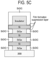
- steps B1 and B2 are performed, as shown in FIGS. 5B and 5C , since the film formation suppression layer formed on the surface of the first material (Si) is maintained on the surface of the first material (Si) as described above, it is possible to suppress the film growth starting from the surface of the first material (Si).
- the film formation suppression layer on the surface of the first material (Si) is insufficient for some reason, the film growth starting from the surface of the first material (Si) may occur very slightly.
- the thickness of the film formed starting from the surface of the first material (Si) is much smaller than the thickness of the film formed starting from the surface of the second material (SiGe). Therefore, even in that case, it is possible to properly bury the inside of the concave portion by the above-mentioned bottom-up growth.
- the wafer 200 is heated and heat-treated to perform post-treatment (PT) on the film formed so as to bury the inside of the concave portion.
- PT post-treatment
- the output of the heater 207 is adjusted so as to make the internal temperature of the process chamber 201, that is, the temperature of the wafer 200 after the film is formed so as to bury the inside of the concave portion, equal to or higher than the temperature of the wafer 200 in steps A and B, preferably higher than the temperature of the wafer 200 in steps A and B.
- PT post-treatment
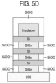
- residual groups or resides of the film formation suppression layer on the surface of the first material (Si), that is, the upper surface of the concave portion and the interface between the side surface of the concave portion and the film (SiOC), can be desorbed by PT. Further, this step may be performed in a state where an inert gas is supplied into the process chamber 201, or may be performed in a state where a reactive substance such as an oxidant (oxidizing gas) is supplied into the process chamber 201. When the reactive substance such as the oxidant is supplied, it is possible to enhance the effect of desorbing the residual groups or residues of the film formation suppression layer on the upper surface of the concave portion and the interface between the side surface of the concave portion and the film.
- the inert gas and the reactive substance such as and the oxidant (oxidizing gas) in this case are also referred to as an assist substance.
- an inert gas acting as a purge gas is supplied into the process chamber 201 from each of the nozzles 249a to 249c and is exhausted through the exhaust port 231a.
- the interior of the process chamber 201 is purged and a gas, reaction by-products, and the like remaining in the process chamber 201 are removed from the interior of the process chamber 201 (after-purging).
- the internal atmosphere of the process chamber 201 is substituted with an inert gas (inert gas substitution) and the internal pressure of the process chamber 201 is returned to the atmospheric pressure (returning to atmospheric pressure).
- the seal cap 219 is moved down by the boat elevator 115 to open the lower end of the manifold 209. Then, the processed wafers 200 supported by the boat 217 are unloaded from the lower end of the manifold 209 to the outside of the reaction tube 203 (boat unloading). After the boat unloading, the shutter 219s is moved and the lower end opening of the manifold 209 is sealed by the shutter 219s via the O-ring 220c (shutter close). The processed wafers 200 are unloaded from the reaction tube 203 and are then discharged from the boat 217 (wafer discharging).
- the film formation suppression layer is formed on the surface of the first material
- the film growth starting from the surface of the first material may occur very slightly for some reason.
- a step of etching an extra film formed on the upper surface of the concave portion or the like may be required.
- the extra film formed on the upper surface of the concave portion or the like is very small as described above, and accordingly, it is possible to significantly reduce the load in the step of etching the extra film and significantly shorten the time required for etching.
- the film (SiOC) is formed on the entire sidewall of the stacked structure in which the second material (SiGe) and the first material (Si) on the surface of the wafer 200 are alternately stacked.
- voids or seams hereinafter, referred to as voids
- the voids formed in the film during film formation are maintained, and in some cases, the voids become deeper due to etching such that the sidewall of the stacked structure in which the second material and the first material are alternately stacked cannot be flattened. Further, when the conventional film forming method is used, it is indispensable to perform the step of etching the extra film, which prolongs the total processing time and lowers the productivity.
- the present embodiment it is possible to form a void-free and seamless film in the concave portion while suppressing the film growth on the upper surface of the concave portion, and further, at the time when the film forming process is completed, the inside of the concave portion in the sidewall of the stacked structure in which the second material (SiGe) and the first material (Si) are alternately stacked can be buried with the film (SiOC) so that the sidewall of the stacked structure can be flattened.
- This makes it possible to omit a step of removing an extra film formed on the upper surface of the concave portion or the like by etching after the film forming process, which is indispensable in the conventional film forming method.
- the film formation suppression layer on the surface of the first material, even if the film growth starting from the surface of the first material occurs very slightly for some reason, an extra film formed on the upper surface of the concave portion or the like is very small, and accordingly, it is possible to significantly reduce the load in the step of etching the extra film and significantly shorten the time required for etching. That is, according to the present embodiment, void-free and seamless burial is possible, which improves the burial characteristics, and further, it is possible to shorten the total processing time due to the omission of the step of etching the extra film or the reduction of the load of the step of etching the extra film, thereby improving the productivity.
- step A By setting the OH termination to be formed on the surface of the first material of the concave portion on the surface of the wafer 200 before performing step A, it is possible to promote adsorption of at least a portion of the molecular structure of molecules constituting the precursor on the surface of the first material of the concave portion, thereby appropriately forming the film formation suppression layer on the surface of the first material.
- the amount (density or concentration) of the OH termination on the surface of the first material (Si) before performing step A to be larger (higher) than the amount (density or concentration) of the OH termination on the surface of the second material (SiGe)
- at least a portion of the molecular structure of molecules constituting the precursor can be selectively (preferentially) adsorbed on the surface of the first material of the first material and the second material of the concave portion, thereby selectively (preferentially) forming the film formation suppression layer on the surface of the first material.
- step A It is also possible to make the surface of the second material not OH-terminated before performing step A, which makes it possible to enhance the selectivity in the selective adsorption of at least the portion of the molecular structure of molecules constituting the precursor on the surface of the first material and the selective formation of the film formation suppression layer on the surface of the first material.
- step C Before performing step A, by performing step C of forming the OH termination on the surface of the first material of the concave portion on the surface of the wafer 200, it is possible to promote the adsorption of at least the portion of the molecular structure of molecules constituting the precursor on the surface of the first material of the concave portion, thereby appropriately forming the film formation suppression layer on the surface of the first material.
- step C by supplying, for example, the oxidant as the reaction material to the wafer 200 to oxidize the surface of the first material, it is possible to form the OH terminations on the surface of the first material with efficiency and good controllability.
- step C the OH termination is also formed on the surface of the second material, but after performing step C and before performing step A, by performing step D of removing the OH termination formed on the surface of the second material, it is possible to create a state in which the OH termination is not formed on the surface of the second material. Further, in step D, by heating and annealing the wafer 200, it is possible to selectively sublimate and remove the oxide such as GeO formed on the surface of the second material (SiGe) while retaining (maintaining) the oxide film such as SiO formed on the surface of the first material (Si).
- step D only by heating the wafer 200, it is possible to selectively remove the OH termination formed on the surface of the second material (SiGe) while retaining (maintaining) the OH termination formed on the surface of the first material (Si).
- the amount (density or concentration) of the OH termination on the surface of the first material (Si) before performing step A can be larger (higher) than the amount (density or concentration) of the OH termination on the surface of the second material (SiGe), it is possible to selectively (preferentially) adsorb at least the portion of the molecular structure of molecules constituting the precursor on the surface of the first material of the first material and the second material of the concave portion, thereby selectively (preferentially) forming the film formation suppression layer on the surface of the first material.
- step D it is also possible to make the surface of the second material not OH-terminated before performing step A, which makes it possible to enhance the selectivity in the selective adsorption of at least the portion of the molecular structure of molecules constituting the precursor on the surface of the first material and the selective formation of the film formation suppression layer on the surface of the first material.
- step E Before performing step C, by performing step E of removing the native oxide film on the surfaces of the first material and the second material of the concave portion on the surface of the wafer 200, it is possible to remove the oxide film that may be formed non-uniformly on the surfaces of the first material and the second material, thereby removing the OH termination that may be formed non-uniformly on the surfaces of the first material and the second material.
- the surface of the first material can be uniformly oxidized, thereby forming the oxide film uniformly on the surface of the first material.
- the OH termination can be uniformly formed on the surface of the first material.
- step B After step B is completed, by performing post-treatment (PT) on the film formed so as to bury the inside of the concave portion with the temperature of the wafer 200 set to be equal to or higher than the temperature of the wafer 200 in step A or step B, preferably higher than the temperature of the wafer 200 in step A or step B, impurities contained in the film formed so as to bury the inside of the concave portion can be removed or defects contained in the film can be repaired. Further, the residual groups or residues of the film formation suppression layer on the surface of the first material, that is, the upper surface of the concave portion and the interface between the side surface of the concave portion and the film, can be desorbed.
- PT post-treatment
- the post-treatment may be performed in a state where an inert gas is supplied into the process chamber 201, or may be performed in a state where a reactive substance such as an oxidant (oxidizing gas) is supplied into the into the process chamber 201.
- a reactive substance such as an oxidant (oxidizing gas) is supplied into the into the process chamber 201.
- the reactive substance such as the oxidant is supplied, it is possible to enhance the effect of desorbing the residual groups or residues of the film formation suppression layer on the upper surface of the concave portion and the interface between the side surface of the concave portion and the film.
- each reaction in each step can proceed under a non-plasma atmosphere, excessive reaction can be suppressed in each step, thereby enhancing the controllability of the reaction. Further, since each step is performed under the non-plasma atmosphere, plasma damage to the wafer 200 can be avoided, so that the present method can be applied to a process in which the plasma damage is a concern.
- the substrate processing sequence in the present embodiment can be changed as in the following modifications. These modifications can be used in proper combination. Unless otherwise stated, the process procedures and process conditions in each step of each modification can be the same as the process procedures and process conditions in each step of the above-described substrate processing sequence.
- step E (native oxide film removal) may be omitted depending on the surface condition of the wafer 200.
- the surface condition of the wafer 200 For example, after forming on the surface of the wafer 200 the stacked structure in FIG. 5A in which the second material (SiGe) and the first material (Si) are alternately stacked, if the surface of the wafer 200 is not exposed to the air, the amount of air exposure is small, or the air exposure time is short, the surface of the first material or the surface of the second material may be in an appropriate surface state.
- step E can be omitted, and the processing sequence can be started from step C (oxidation). This modification can also obtain the same effects as the above-described embodiment.
- step E it is possible to shorten the total processing time and improve the productivity.
- step E native oxide film removal
- step C oxidation
- steps E and C can be omitted, and the processing sequence can be started from step D (ANL).
- This modification can also obtain the same effects as the above-described embodiment.
- steps E and C it is possible to shorten the total processing time and improve the productivity.
- step E native oxide film removal
- step C oxidation
- step D ANL
- step E native oxide film removal
- step C oxidation
- step D step D
- the oxide film is uniformly formed on the surfaces of the first material (Si) and the second material (SiGe) on the surface of the wafer 200 and the wafer 200 is heated to a temperature of, for example, 100 degrees C in step A (film formation suppression layer formation)
- the oxide such as GeO formed on the surface of the second material can be sublimated and removed while retaining (maintaining) the oxide film such as the SiO film formed on the surface of the first material.
- step A the OH terminal formed on the surface of the second material can be removed while retaining (maintaining) the OH terminal formed on the surface of the first material.
- steps E, C, and D can be omitted, and the processing sequence can be started from step A.
- This modification can also obtain the same effects as the above-described embodiment. Further, by omitting steps E, C, and D, it is possible to shorten the total processing time and improve the productivity.
- the raw material may be supplied alone without supplying the catalyst to the wafer 200.
- the oxidant may be supplied alone without supplying the catalyst to the wafer 200.
- the supply of the catalyst can be omitted when the chemical adsorption of at least the portion of the molecular structure of molecules constituting the raw material on the surface of the second material or the oxidation rate is adjusted by the temperature.
- This modification can also obtain the same effects as the above-described embodiment.
- step F may be omitted.
- step F can be omitted.
- step F can be omitted.
- step F can be omitted.
- step F can be omitted when the film formation suppression layer or the like is allowed to remain on the upper surface of the concave portion and the interface between the side surface of the concave portion and the film, or even when the amount of residual groups, residues, and the like of the film formation suppression layer on the upper surface of the concave portion and the interface between the side surface of the concave portion and the film is within an allowable range.
- step F can be omitted. This modification can also obtain the same effects as the above-described embodiment. Further, by omitting step F, it is possible to shorten the total processing time and improve the productivity.
- the etchant may be plasma-excited and supplied to the wafer 200.
- the reaction material such as the oxidant may be plasma-excited and supplied to the wafer 200.
- the inert gas may be plasma-excited and supplied. This makes it possible to remove the oxide such as Geo formed on the surface of the second material by sublimation, and at the same time, treat the surface of the second material after the oxide is removed.
- the assist substance may be plasma-excited and supplied. This makes it possible to further enhance the effect of desorbing the residual groups or residues of the film formation suppression layer on the upper surface of the concave portion and the interface between the side surface of the concave portion and the film.
- a silicon-based oxide film such as a silicon oxycarbonitride film (SiOCN film), a silicon oxynitride film (SiON film), a silicon oxyboronitride film (SiBON film), or a silicon oxyborocarbonitride film (SiBOCN film) may be formed.
- a metal-based oxide film such as an aluminum oxide film (AlO film), a titanium oxide film (TiO film), a hafnium oxide film (HfO film), or a zirconium oxide film (ZrO film) may be formed.
- Recipes used in each process may be prepared individually according to the processing contents and may be stored in the memory 121c via a telecommunication line or the external memory 123. Moreover, at the beginning of each process, the CPU 121a may properly select an appropriate recipe from the recipes stored in the memory 121c according to the processing contents. Thus, it is possible for a single substrate processing apparatus to form films of various kinds, composition ratios, qualities, and thicknesses with enhanced reproducibility. Further, it is possible to reduce an operator's burden and to quickly start each process while avoiding an operation error.
- the recipes mentioned above are not limited to newly-prepared ones but may be prepared, for example, by modifying existing recipes that are already installed in the substrate processing apparatus. Once the recipes are modified, the modified recipes may be installed in the substrate processing apparatus via a telecommunication line or a recording medium storing the recipes. In addition, the existing recipes already installed in the existing substrate processing apparatus may be directly modified by operating the input/output device 122 of the substrate processing apparatus.
- each process may be performed according to the same processing procedures and process conditions as those in the above-described embodiments, and the same effects as the above-described embodiments are achieved.
- FIG. 5A by performing the processing sequence of the above-described embodiment on a wafer having a stacked structure in which a SiGe film and a Si film are alternately stacked on the surface of the wafer and having a concave portion with its upper surface and side surface composed of the Si film and its bottom surface composed of the SiGe film, whose depth direction is a direction (horizontal direction) parallel to the surface of the wafer, a SiOC film was formed so as to bury the inside of the concave portion to prepare Evaluation Sample 1. Then, a cross-sectional TEM image of Evaluation Sample 1 was taken.
- FIG. 7 shows the cross-sectional TEM image of Evaluation Sample 1.
- FIG. 8 shows the cross-sectional TEM image of Evaluation Sample 2.
- Evaluation Sample 1 As shown in FIG. 7 , in Evaluation Sample 1, it can be seen that the SiOC film is selectively formed only in the inside of the concave portion without being formed on the upper surface of the concave portion. Further, it can be seen that voids and seams are not generated in the SiOC film formed in the inside of the concave portion.
- Evaluation Sample 2 As shown in FIG. 8 , in Evaluation Sample 2, it can be seen that a void-free and seamless SiOC film is formed so as to bury the inside of the concave portion. Further, in Evaluation Sample 2, although the SiOC film is slightly formed on the upper surface of the concave portion, it can be seen that the SiOC film has a flat profile on the sidewall of the stacked structure in which the SiGe film and the Si film are alternately stacked.
- the SiOC film formed on the sidewall of the stacked structure in which the SiGe film and the Si film are alternately stacked by the thickness of the SiOC film formed on the upper surface of the concave portion, the Si film on the sidewall of the stacked structure, that is, the upper surface (Si) of the concave portion, can be exposed while keeping the sidewall of the stacked structure flat.
Landscapes
- Chemical & Material Sciences (AREA)
- General Chemical & Material Sciences (AREA)
- Chemical Kinetics & Catalysis (AREA)
- Engineering & Computer Science (AREA)
- Materials Engineering (AREA)
- Mechanical Engineering (AREA)
- Metallurgy (AREA)
- Organic Chemistry (AREA)
- Inorganic Chemistry (AREA)
- Chemical Vapour Deposition (AREA)
- Formation Of Insulating Films (AREA)
- Recrystallisation Techniques (AREA)
- Semiconductor Memories (AREA)
- Design And Manufacture Of Integrated Circuits (AREA)
Applications Claiming Priority (2)
| Application Number | Priority Date | Filing Date | Title |
|---|---|---|---|
| JP2021070590A JP7305700B2 (ja) | 2021-04-19 | 2021-04-19 | 基板処理方法、半導体装置の製造方法、基板処理装置、およびプログラム |
| EP22162524.7A EP4080548B1 (de) | 2021-04-19 | 2022-03-16 | Verfahren zur verarbeitung eines substrats, verfahren zur herstellung eines halbleiterbauelements, substratverarbeitungsgerät und programm |
Related Parent Applications (2)
| Application Number | Title | Priority Date | Filing Date |
|---|---|---|---|
| EP22162524.7A Division-Into EP4080548B1 (de) | 2021-04-19 | 2022-03-16 | Verfahren zur verarbeitung eines substrats, verfahren zur herstellung eines halbleiterbauelements, substratverarbeitungsgerät und programm |
| EP22162524.7A Division EP4080548B1 (de) | 2021-04-19 | 2022-03-16 | Verfahren zur verarbeitung eines substrats, verfahren zur herstellung eines halbleiterbauelements, substratverarbeitungsgerät und programm |
Publications (2)
| Publication Number | Publication Date |
|---|---|
| EP4538414A2 true EP4538414A2 (de) | 2025-04-16 |
| EP4538414A3 EP4538414A3 (de) | 2025-07-02 |
Family
ID=81326236
Family Applications (2)
| Application Number | Title | Priority Date | Filing Date |
|---|---|---|---|
| EP25159603.7A Pending EP4538414A3 (de) | 2021-04-19 | 2022-03-16 | Verfahren zur substratverarbeitung, verfahren zur herstellung eines halbleiterbauelements, substratverarbeitungsvorrichtung und programm |
| EP22162524.7A Active EP4080548B1 (de) | 2021-04-19 | 2022-03-16 | Verfahren zur verarbeitung eines substrats, verfahren zur herstellung eines halbleiterbauelements, substratverarbeitungsgerät und programm |
Family Applications After (1)
| Application Number | Title | Priority Date | Filing Date |
|---|---|---|---|
| EP22162524.7A Active EP4080548B1 (de) | 2021-04-19 | 2022-03-16 | Verfahren zur verarbeitung eines substrats, verfahren zur herstellung eines halbleiterbauelements, substratverarbeitungsgerät und programm |
Country Status (6)
| Country | Link |
|---|---|
| US (4) | US11626280B2 (de) |
| EP (2) | EP4538414A3 (de) |
| JP (3) | JP7305700B2 (de) |
| KR (3) | KR102753914B1 (de) |
| CN (1) | CN115224102A (de) |
| TW (2) | TWI900901B (de) |
Families Citing this family (4)
| Publication number | Priority date | Publication date | Assignee | Title |
|---|---|---|---|---|
| JP7305700B2 (ja) * | 2021-04-19 | 2023-07-10 | 株式会社Kokusai Electric | 基板処理方法、半導体装置の製造方法、基板処理装置、およびプログラム |
| JP7374961B2 (ja) * | 2021-07-27 | 2023-11-07 | 株式会社Kokusai Electric | 半導体装置の製造方法、基板処理方法、基板処理装置、およびプログラム |
| JP2026020791A (ja) | 2024-07-29 | 2026-02-10 | 株式会社Kokusai Electric | 基板処理方法、半導体装置の製造方法、プログラム、および基板処理装置 |
| JP2026027885A (ja) | 2024-08-06 | 2026-02-19 | 東京エレクトロン株式会社 | 基板処理方法、半導体装置の製造方法及びマイクロ波プラズマ装置 |
Family Cites Families (33)
| Publication number | Priority date | Publication date | Assignee | Title |
|---|---|---|---|---|
| US6391785B1 (en) | 1999-08-24 | 2002-05-21 | Interuniversitair Microelektronica Centrum (Imec) | Method for bottomless deposition of barrier layers in integrated circuit metallization schemes |
| US7625820B1 (en) | 2006-06-21 | 2009-12-01 | Novellus Systems, Inc. | Method of selective coverage of high aspect ratio structures with a conformal film |
| US20080242097A1 (en) * | 2007-03-28 | 2008-10-02 | Tim Boescke | Selective deposition method |
| JP6155063B2 (ja) | 2013-03-19 | 2017-06-28 | 株式会社日立国際電気 | 半導体装置の製造方法、基板処理装置及びプログラム |
| JP6100854B2 (ja) * | 2014-11-19 | 2017-03-22 | 株式会社日立国際電気 | 半導体装置の製造方法、基板処理装置、ガス供給システムおよびプログラム |
| US9553100B2 (en) | 2014-12-04 | 2017-01-24 | Sandisk Techologies Llc | Selective floating gate semiconductor material deposition in a three-dimensional memory structure |
| JP6436887B2 (ja) | 2015-09-30 | 2018-12-12 | 株式会社Kokusai Electric | 半導体装置の製造方法、基板処理装置、ガス供給システムおよびプログラム |
| KR20180069038A (ko) * | 2015-11-13 | 2018-06-22 | 어플라이드 머티어리얼스, 인코포레이티드 | 선택적 표면 개질을 이용하여 구조를 충전하기 위한 기술들 |
| KR102577628B1 (ko) | 2016-01-05 | 2023-09-13 | 어플라이드 머티어리얼스, 인코포레이티드 | 반도체 응용들을 위한 수평 게이트 올 어라운드 디바이스들을 위한 나노와이어들을 제조하기 위한 방법 |
| CN109075072B (zh) | 2016-05-20 | 2023-11-03 | 株式会社国际电气 | 清洁方法、半导体器件的制造方法、衬底处理装置及程序 |
| JP2017222928A (ja) | 2016-05-31 | 2017-12-21 | 東京エレクトロン株式会社 | 表面処理による選択的堆積 |
| KR102112705B1 (ko) * | 2016-12-09 | 2020-05-21 | 주식회사 원익아이피에스 | 박막 증착 방법 |
| TWI700750B (zh) * | 2017-01-24 | 2020-08-01 | 美商應用材料股份有限公司 | 用於介電薄膜的選擇性沉積之方法及設備 |
| JP7085561B2 (ja) * | 2017-03-17 | 2022-06-16 | バーサム マテリアルズ ユーエス,リミティド ライアビリティ カンパニー | ケイ素含有表面への選択的堆積 |
| TWI850084B (zh) * | 2017-06-14 | 2024-07-21 | 美商應用材料股份有限公司 | 用於達成無缺陷自組裝單層的晶圓處理設備 |
| US10269571B2 (en) * | 2017-07-12 | 2019-04-23 | Applied Materials, Inc. | Methods for fabricating nanowire for semiconductor applications |
| US10651291B2 (en) * | 2017-08-18 | 2020-05-12 | Globalfoundries Inc. | Inner spacer formation in a nanosheet field-effect transistor |
| WO2019039127A1 (ja) * | 2017-08-22 | 2019-02-28 | 株式会社日立国際電気 | 半導体装置の製造方法、基板処理装置およびプログラム |
| US11371136B2 (en) | 2017-09-19 | 2022-06-28 | Applied Materials, Inc. | Methods for selective deposition of dielectric on silicon oxide |
| US10553679B2 (en) * | 2017-12-07 | 2020-02-04 | International Business Machines Corporation | Formation of self-limited inner spacer for gate-all-around nanosheet FET |
| JP7194525B2 (ja) | 2017-12-28 | 2022-12-22 | 東京応化工業株式会社 | 表面処理方法、表面処理剤、及び基板上に領域選択的に製膜する方法 |
| US10535733B2 (en) * | 2018-01-11 | 2020-01-14 | International Business Machines Corporation | Method of forming a nanosheet transistor |
| JP7040257B2 (ja) | 2018-04-25 | 2022-03-23 | 東京エレクトロン株式会社 | 成膜装置、及び成膜方法 |
| JP2019204815A (ja) * | 2018-05-21 | 2019-11-28 | 東京エレクトロン株式会社 | 基板処理方法及び基板処理装置 |
| US11114306B2 (en) | 2018-09-17 | 2021-09-07 | Applied Materials, Inc. | Methods for depositing dielectric material |
| JP2020056104A (ja) | 2018-10-02 | 2020-04-09 | エーエスエム アイピー ホールディング ビー.ブイ. | 選択的パッシベーションおよび選択的堆積 |
| US10593695B1 (en) * | 2018-10-17 | 2020-03-17 | Micron Technology, Inc. | Integrated assemblies having charge-trapping material arranged in vertically-spaced segments, and methods of forming integrated assemblies |
| US10832907B2 (en) * | 2019-02-15 | 2020-11-10 | International Business Machines Corporation | Gate-all-around field-effect transistor devices having source/drain extension contacts to channel layers for reduced parasitic resistance |
| JP6960953B2 (ja) * | 2019-03-20 | 2021-11-05 | 株式会社Kokusai Electric | 半導体装置の製造方法、基板処理方法、基板処理装置、およびプログラム |
| JP7023905B2 (ja) * | 2019-08-30 | 2022-02-22 | 株式会社Kokusai Electric | 半導体装置の製造方法、基板処理方法、基板処理装置、およびプログラム |
| JP2021040060A (ja) * | 2019-09-04 | 2021-03-11 | 株式会社Kokusai Electric | 半導体装置の製造方法、基板処理システム、およびプログラム |
| JP2021052034A (ja) * | 2019-09-20 | 2021-04-01 | 東京エレクトロン株式会社 | 金属酸化物膜の形成方法及び成膜装置 |
| JP7305700B2 (ja) * | 2021-04-19 | 2023-07-10 | 株式会社Kokusai Electric | 基板処理方法、半導体装置の製造方法、基板処理装置、およびプログラム |
-
2021
- 2021-04-19 JP JP2021070590A patent/JP7305700B2/ja active Active
-
2022
- 2022-01-27 TW TW112138194A patent/TWI900901B/zh active
- 2022-01-27 TW TW111103484A patent/TWI821885B/zh active
- 2022-02-14 CN CN202210132429.0A patent/CN115224102A/zh active Pending
- 2022-03-16 EP EP25159603.7A patent/EP4538414A3/de active Pending
- 2022-03-16 EP EP22162524.7A patent/EP4080548B1/de active Active
- 2022-03-17 US US17/697,533 patent/US11626280B2/en active Active
- 2022-03-17 KR KR1020220033116A patent/KR102753914B1/ko active Active
- 2022-12-14 US US18/081,277 patent/US11935742B2/en active Active
-
2023
- 2023-06-28 JP JP2023105614A patent/JP7640620B2/ja active Active
-
2024
- 2024-01-25 US US18/422,641 patent/US12283478B2/en active Active
-
2025
- 2025-01-08 KR KR1020250002699A patent/KR102903301B1/ko active Active
- 2025-02-20 JP JP2025025825A patent/JP2025076518A/ja active Pending
- 2025-03-31 US US19/095,859 patent/US20250226204A1/en active Pending
- 2025-12-18 KR KR1020250202692A patent/KR20260002506A/ko active Pending
Also Published As
| Publication number | Publication date |
|---|---|
| TW202242180A (zh) | 2022-11-01 |
| KR20250011989A (ko) | 2025-01-22 |
| JP2025076518A (ja) | 2025-05-15 |
| US12283478B2 (en) | 2025-04-22 |
| JP7640620B2 (ja) | 2025-03-05 |
| US20230123702A1 (en) | 2023-04-20 |
| EP4080548B1 (de) | 2026-04-29 |
| JP7305700B2 (ja) | 2023-07-10 |
| US20250226204A1 (en) | 2025-07-10 |
| JP2022165287A (ja) | 2022-10-31 |
| CN115224102A (zh) | 2022-10-21 |
| KR102753914B1 (ko) | 2025-01-14 |
| TWI900901B (zh) | 2025-10-11 |
| KR20220144311A (ko) | 2022-10-26 |
| TW202417671A (zh) | 2024-05-01 |
| US20220336213A1 (en) | 2022-10-20 |
| US11935742B2 (en) | 2024-03-19 |
| KR20260002506A (ko) | 2026-01-06 |
| EP4080548A1 (de) | 2022-10-26 |
| KR102903301B1 (ko) | 2025-12-24 |
| JP2023123717A (ja) | 2023-09-05 |
| US11626280B2 (en) | 2023-04-11 |
| EP4538414A3 (de) | 2025-07-02 |
| TWI821885B (zh) | 2023-11-11 |
| US20240170280A1 (en) | 2024-05-23 |
Similar Documents
| Publication | Publication Date | Title |
|---|---|---|
| EP4538414A2 (de) | Verfahren zur substratverarbeitung, verfahren zur herstellung eines halbleiterbauelements, substratverarbeitungsvorrichtung und programm | |
| US12331393B2 (en) | Method of processing substrate, method of manufacturing semiconductor device, substrate processing apparatus, and recording medium | |
| EP4124673A1 (de) | Verfahren zur verarbeitung eines substrats, verfahren zur herstellung eines halbleiterbauelements, substratverarbeitungsgerät und programm | |
| US12525450B2 (en) | Method of processing substrate, method of manufacturing semiconductor device, substrate processing apparatus, and recording medium | |
| EP4245883A1 (de) | Verfahren zur substratverarbeitung, verfahren zur herstellung eines halbleiterbauelements, substratverarbeitungsvorrichtung und programm | |
| US20240254625A1 (en) | Method of processing substrate, method of manufacturing semiconductor device, substrate processing apparatus, and recording medium | |
| EP4340003A1 (de) | Verfahren zur substratverarbeitung, verfahren zur herstellung eines halbleiterbauelements, substratverarbeitungsvorrichtung und programm | |
| EP4343816A1 (de) | Verfahren zur substratverarbeitung, verfahren zur herstellung eines halbleiterbauelements, substratverarbeitungssystem und programm | |
| JP7654610B2 (ja) | 基板処理方法、半導体装置の製造方法、プログラム、および基板処理装置 | |
| EP4343815A1 (de) | Verfahren zur substratverarbeitung, verfahren zur herstellung eines halbleiterbauelements, substratverarbeitungssystem und programm |
Legal Events
| Date | Code | Title | Description |
|---|---|---|---|
| PUAI | Public reference made under article 153(3) epc to a published international application that has entered the european phase |
Free format text: ORIGINAL CODE: 0009012 |
|
| STAA | Information on the status of an ep patent application or granted ep patent |
Free format text: STATUS: REQUEST FOR EXAMINATION WAS MADE |
|
| 17P | Request for examination filed |
Effective date: 20250224 |
|
| AC | Divisional application: reference to earlier application |
Ref document number: 4080548 Country of ref document: EP Kind code of ref document: P |
|
| AK | Designated contracting states |
Kind code of ref document: A2 Designated state(s): AL AT BE BG CH CY CZ DE DK EE ES FI FR GB GR HR HU IE IS IT LI LT LU LV MC MK MT NL NO PL PT RO RS SE SI SK SM TR |
|
| REG | Reference to a national code |
Ref country code: DE Ref legal event code: R079 Free format text: PREVIOUS MAIN CLASS: C23C0016455000 Ipc: H01L0021020000 |
|
| PUAL | Search report despatched |
Free format text: ORIGINAL CODE: 0009013 |
|
| AK | Designated contracting states |
Kind code of ref document: A3 Designated state(s): AL AT BE BG CH CY CZ DE DK EE ES FI FR GB GR HR HU IE IS IT LI LT LU LV MC MK MT NL NO PL PT RO RS SE SI SK SM TR |
|
| RIC1 | Information provided on ipc code assigned before grant |
Ipc: H01L 21/32 20060101ALI20250528BHEP Ipc: H01L 21/02 20060101AFI20250528BHEP |