EP4398301A2 - Substrat für eine anzeigevorrichtung und anzeigevorrichtung damit - Google Patents
Substrat für eine anzeigevorrichtung und anzeigevorrichtung damit Download PDFInfo
- Publication number
- EP4398301A2 EP4398301A2 EP24178116.0A EP24178116A EP4398301A2 EP 4398301 A2 EP4398301 A2 EP 4398301A2 EP 24178116 A EP24178116 A EP 24178116A EP 4398301 A2 EP4398301 A2 EP 4398301A2
- Authority
- EP
- European Patent Office
- Prior art keywords
- electrode
- tft
- display device
- gate
- insulation film
- Prior art date
- Legal status (The legal status is an assumption and is not a legal conclusion. Google has not performed a legal analysis and makes no representation as to the accuracy of the status listed.)
- Pending
Links
Images


Classifications
-
- G—PHYSICS
- G09—EDUCATION; CRYPTOGRAPHY; DISPLAY; ADVERTISING; SEALS
- G09G—ARRANGEMENTS OR CIRCUITS FOR CONTROL OF INDICATING DEVICES USING STATIC MEANS TO PRESENT VARIABLE INFORMATION
- G09G3/00—Control arrangements or circuits, of interest only in connection with visual indicators other than cathode-ray tubes
- G09G3/20—Control arrangements or circuits, of interest only in connection with visual indicators other than cathode-ray tubes for presentation of an assembly of a number of characters, e.g. a page, by composing the assembly by combination of individual elements arranged in a matrix no fixed position being assigned to or needed to be assigned to the individual characters or partial characters
- G09G3/22—Control arrangements or circuits, of interest only in connection with visual indicators other than cathode-ray tubes for presentation of an assembly of a number of characters, e.g. a page, by composing the assembly by combination of individual elements arranged in a matrix no fixed position being assigned to or needed to be assigned to the individual characters or partial characters using controlled light sources
- G09G3/30—Control arrangements or circuits, of interest only in connection with visual indicators other than cathode-ray tubes for presentation of an assembly of a number of characters, e.g. a page, by composing the assembly by combination of individual elements arranged in a matrix no fixed position being assigned to or needed to be assigned to the individual characters or partial characters using controlled light sources using electroluminescent panels
- G09G3/32—Control arrangements or circuits, of interest only in connection with visual indicators other than cathode-ray tubes for presentation of an assembly of a number of characters, e.g. a page, by composing the assembly by combination of individual elements arranged in a matrix no fixed position being assigned to or needed to be assigned to the individual characters or partial characters using controlled light sources using electroluminescent panels semiconductive, e.g. using light-emitting diodes [LED]
- G09G3/3208—Control arrangements or circuits, of interest only in connection with visual indicators other than cathode-ray tubes for presentation of an assembly of a number of characters, e.g. a page, by composing the assembly by combination of individual elements arranged in a matrix no fixed position being assigned to or needed to be assigned to the individual characters or partial characters using controlled light sources using electroluminescent panels semiconductive, e.g. using light-emitting diodes [LED] organic, e.g. using organic light-emitting diodes [OLED]
- G09G3/3225—Control arrangements or circuits, of interest only in connection with visual indicators other than cathode-ray tubes for presentation of an assembly of a number of characters, e.g. a page, by composing the assembly by combination of individual elements arranged in a matrix no fixed position being assigned to or needed to be assigned to the individual characters or partial characters using controlled light sources using electroluminescent panels semiconductive, e.g. using light-emitting diodes [LED] organic, e.g. using organic light-emitting diodes [OLED] using an active matrix
-
- H—ELECTRICITY
- H10—SEMICONDUCTOR DEVICES; ELECTRIC SOLID-STATE DEVICES NOT OTHERWISE PROVIDED FOR
- H10D—INORGANIC ELECTRIC SEMICONDUCTOR DEVICES
- H10D1/00—Resistors, capacitors or inductors
- H10D1/60—Capacitors
- H10D1/68—Capacitors having no potential barriers
-
- H—ELECTRICITY
- H10—SEMICONDUCTOR DEVICES; ELECTRIC SOLID-STATE DEVICES NOT OTHERWISE PROVIDED FOR
- H10D—INORGANIC ELECTRIC SEMICONDUCTOR DEVICES
- H10D86/00—Integrated devices formed in or on insulating or conducting substrates, e.g. formed in silicon-on-insulator [SOI] substrates or on stainless steel or glass substrates
- H10D86/40—Integrated devices formed in or on insulating or conducting substrates, e.g. formed in silicon-on-insulator [SOI] substrates or on stainless steel or glass substrates characterised by multiple TFTs
- H10D86/421—Integrated devices formed in or on insulating or conducting substrates, e.g. formed in silicon-on-insulator [SOI] substrates or on stainless steel or glass substrates characterised by multiple TFTs having a particular composition, shape or crystalline structure of the active layer
- H10D86/423—Integrated devices formed in or on insulating or conducting substrates, e.g. formed in silicon-on-insulator [SOI] substrates or on stainless steel or glass substrates characterised by multiple TFTs having a particular composition, shape or crystalline structure of the active layer comprising semiconductor materials not belonging to the Group IV, e.g. InGaZnO
-
- H—ELECTRICITY
- H10—SEMICONDUCTOR DEVICES; ELECTRIC SOLID-STATE DEVICES NOT OTHERWISE PROVIDED FOR
- H10D—INORGANIC ELECTRIC SEMICONDUCTOR DEVICES
- H10D86/00—Integrated devices formed in or on insulating or conducting substrates, e.g. formed in silicon-on-insulator [SOI] substrates or on stainless steel or glass substrates
- H10D86/40—Integrated devices formed in or on insulating or conducting substrates, e.g. formed in silicon-on-insulator [SOI] substrates or on stainless steel or glass substrates characterised by multiple TFTs
- H10D86/451—Integrated devices formed in or on insulating or conducting substrates, e.g. formed in silicon-on-insulator [SOI] substrates or on stainless steel or glass substrates characterised by multiple TFTs characterised by the compositions or shapes of the interlayer dielectrics
-
- H—ELECTRICITY
- H10—SEMICONDUCTOR DEVICES; ELECTRIC SOLID-STATE DEVICES NOT OTHERWISE PROVIDED FOR
- H10D—INORGANIC ELECTRIC SEMICONDUCTOR DEVICES
- H10D86/00—Integrated devices formed in or on insulating or conducting substrates, e.g. formed in silicon-on-insulator [SOI] substrates or on stainless steel or glass substrates
- H10D86/40—Integrated devices formed in or on insulating or conducting substrates, e.g. formed in silicon-on-insulator [SOI] substrates or on stainless steel or glass substrates characterised by multiple TFTs
- H10D86/471—Integrated devices formed in or on insulating or conducting substrates, e.g. formed in silicon-on-insulator [SOI] substrates or on stainless steel or glass substrates characterised by multiple TFTs having different architectures, e.g. having both top-gate and bottom-gate TFTs
-
- H—ELECTRICITY
- H10—SEMICONDUCTOR DEVICES; ELECTRIC SOLID-STATE DEVICES NOT OTHERWISE PROVIDED FOR
- H10D—INORGANIC ELECTRIC SEMICONDUCTOR DEVICES
- H10D86/00—Integrated devices formed in or on insulating or conducting substrates, e.g. formed in silicon-on-insulator [SOI] substrates or on stainless steel or glass substrates
- H10D86/40—Integrated devices formed in or on insulating or conducting substrates, e.g. formed in silicon-on-insulator [SOI] substrates or on stainless steel or glass substrates characterised by multiple TFTs
- H10D86/481—Integrated devices formed in or on insulating or conducting substrates, e.g. formed in silicon-on-insulator [SOI] substrates or on stainless steel or glass substrates characterised by multiple TFTs integrated with passive devices, e.g. auxiliary capacitors
-
- H—ELECTRICITY
- H10—SEMICONDUCTOR DEVICES; ELECTRIC SOLID-STATE DEVICES NOT OTHERWISE PROVIDED FOR
- H10D—INORGANIC ELECTRIC SEMICONDUCTOR DEVICES
- H10D86/00—Integrated devices formed in or on insulating or conducting substrates, e.g. formed in silicon-on-insulator [SOI] substrates or on stainless steel or glass substrates
- H10D86/40—Integrated devices formed in or on insulating or conducting substrates, e.g. formed in silicon-on-insulator [SOI] substrates or on stainless steel or glass substrates characterised by multiple TFTs
- H10D86/60—Integrated devices formed in or on insulating or conducting substrates, e.g. formed in silicon-on-insulator [SOI] substrates or on stainless steel or glass substrates characterised by multiple TFTs wherein the TFTs are in active matrices
-
- H—ELECTRICITY
- H10—SEMICONDUCTOR DEVICES; ELECTRIC SOLID-STATE DEVICES NOT OTHERWISE PROVIDED FOR
- H10K—ORGANIC ELECTRIC SOLID-STATE DEVICES
- H10K59/00—Integrated devices, or assemblies of multiple devices, comprising at least one organic light-emitting element covered by group H10K50/00
- H10K59/10—OLED displays
- H10K59/12—Active-matrix OLED [AMOLED] displays
- H10K59/121—Active-matrix OLED [AMOLED] displays characterised by the geometry or disposition of pixel elements
- H10K59/1213—Active-matrix OLED [AMOLED] displays characterised by the geometry or disposition of pixel elements the pixel elements being TFTs
-
- H—ELECTRICITY
- H10—SEMICONDUCTOR DEVICES; ELECTRIC SOLID-STATE DEVICES NOT OTHERWISE PROVIDED FOR
- H10K—ORGANIC ELECTRIC SOLID-STATE DEVICES
- H10K59/00—Integrated devices, or assemblies of multiple devices, comprising at least one organic light-emitting element covered by group H10K50/00
- H10K59/10—OLED displays
- H10K59/12—Active-matrix OLED [AMOLED] displays
- H10K59/121—Active-matrix OLED [AMOLED] displays characterised by the geometry or disposition of pixel elements
- H10K59/1216—Active-matrix OLED [AMOLED] displays characterised by the geometry or disposition of pixel elements the pixel elements being capacitors
-
- H—ELECTRICITY
- H10—SEMICONDUCTOR DEVICES; ELECTRIC SOLID-STATE DEVICES NOT OTHERWISE PROVIDED FOR
- H10K—ORGANIC ELECTRIC SOLID-STATE DEVICES
- H10K59/00—Integrated devices, or assemblies of multiple devices, comprising at least one organic light-emitting element covered by group H10K50/00
- H10K59/10—OLED displays
- H10K59/12—Active-matrix OLED [AMOLED] displays
- H10K59/129—Chiplets
-
- H—ELECTRICITY
- H10—SEMICONDUCTOR DEVICES; ELECTRIC SOLID-STATE DEVICES NOT OTHERWISE PROVIDED FOR
- H10K—ORGANIC ELECTRIC SOLID-STATE DEVICES
- H10K59/00—Integrated devices, or assemblies of multiple devices, comprising at least one organic light-emitting element covered by group H10K50/00
- H10K59/10—OLED displays
- H10K59/12—Active-matrix OLED [AMOLED] displays
- H10K59/131—Interconnections, e.g. wiring lines or terminals
-
- G—PHYSICS
- G09—EDUCATION; CRYPTOGRAPHY; DISPLAY; ADVERTISING; SEALS
- G09G—ARRANGEMENTS OR CIRCUITS FOR CONTROL OF INDICATING DEVICES USING STATIC MEANS TO PRESENT VARIABLE INFORMATION
- G09G2310/00—Command of the display device
- G09G2310/02—Addressing, scanning or driving the display screen or processing steps related thereto
- G09G2310/0264—Details of driving circuits
- G09G2310/0297—Special arrangements with multiplexing or demultiplexing of display data in the drivers for data electrodes, in a pre-processing circuitry delivering display data to said drivers or in the matrix panel, e.g. multiplexing plural data signals to one D/A converter or demultiplexing the D/A converter output to multiple columns
-
- H—ELECTRICITY
- H10—SEMICONDUCTOR DEVICES; ELECTRIC SOLID-STATE DEVICES NOT OTHERWISE PROVIDED FOR
- H10D—INORGANIC ELECTRIC SEMICONDUCTOR DEVICES
- H10D30/00—Field-effect transistors [FET]
- H10D30/60—Insulated-gate field-effect transistors [IGFET]
- H10D30/67—Thin-film transistors [TFT]
- H10D30/6729—Thin-film transistors [TFT] characterised by the electrodes
- H10D30/673—Thin-film transistors [TFT] characterised by the electrodes characterised by the shapes, relative sizes or dispositions of the gate electrodes
- H10D30/6731—Top-gate only TFTs
-
- H—ELECTRICITY
- H10—SEMICONDUCTOR DEVICES; ELECTRIC SOLID-STATE DEVICES NOT OTHERWISE PROVIDED FOR
- H10D—INORGANIC ELECTRIC SEMICONDUCTOR DEVICES
- H10D30/00—Field-effect transistors [FET]
- H10D30/60—Insulated-gate field-effect transistors [IGFET]
- H10D30/67—Thin-film transistors [TFT]
- H10D30/674—Thin-film transistors [TFT] characterised by the active materials
- H10D30/6741—Group IV materials, e.g. germanium or silicon carbide
- H10D30/6743—Silicon
- H10D30/6745—Polycrystalline or microcrystalline silicon
-
- H—ELECTRICITY
- H10—SEMICONDUCTOR DEVICES; ELECTRIC SOLID-STATE DEVICES NOT OTHERWISE PROVIDED FOR
- H10D—INORGANIC ELECTRIC SEMICONDUCTOR DEVICES
- H10D30/00—Field-effect transistors [FET]
- H10D30/60—Insulated-gate field-effect transistors [IGFET]
- H10D30/67—Thin-film transistors [TFT]
- H10D30/674—Thin-film transistors [TFT] characterised by the active materials
- H10D30/6755—Oxide semiconductors, e.g. zinc oxide, copper aluminium oxide or cadmium stannate
-
- H—ELECTRICITY
- H10—SEMICONDUCTOR DEVICES; ELECTRIC SOLID-STATE DEVICES NOT OTHERWISE PROVIDED FOR
- H10K—ORGANIC ELECTRIC SOLID-STATE DEVICES
- H10K59/00—Integrated devices, or assemblies of multiple devices, comprising at least one organic light-emitting element covered by group H10K50/00
- H10K59/10—OLED displays
- H10K59/12—Active-matrix OLED [AMOLED] displays
- H10K59/1201—Manufacture or treatment
-
- H—ELECTRICITY
- H10—SEMICONDUCTOR DEVICES; ELECTRIC SOLID-STATE DEVICES NOT OTHERWISE PROVIDED FOR
- H10K—ORGANIC ELECTRIC SOLID-STATE DEVICES
- H10K59/00—Integrated devices, or assemblies of multiple devices, comprising at least one organic light-emitting element covered by group H10K50/00
- H10K59/10—OLED displays
- H10K59/12—Active-matrix OLED [AMOLED] displays
- H10K59/122—Pixel-defining structures or layers, e.g. banks
-
- H—ELECTRICITY
- H10—SEMICONDUCTOR DEVICES; ELECTRIC SOLID-STATE DEVICES NOT OTHERWISE PROVIDED FOR
- H10K—ORGANIC ELECTRIC SOLID-STATE DEVICES
- H10K59/00—Integrated devices, or assemblies of multiple devices, comprising at least one organic light-emitting element covered by group H10K50/00
- H10K59/10—OLED displays
- H10K59/12—Active-matrix OLED [AMOLED] displays
- H10K59/126—Shielding, e.g. light-blocking means over the TFTs
Definitions
- the present disclosure is directed to a substrate for a display device and a display device including the same that substantially obviate one or more problems due to limitations and disadvantages of the related art.
- Embodiments relate to a display device.
- the display device includes a substrate and a pixel on the substrate.
- the pixel includes a first thin-film transistor (TFT) on the substrate, a storage capacitor on the substrate, and a light-emitting device electrically connected to the storage capacitor.
- the first TFT includes a first gate electrode, at least a first part of an interlayer insulation film on the first gate electrode, a first gate insulation film on the first part of the interlayer insulation film, and a first active layer formed of oxide semiconductor on the first gate insulation film.
- the storage capacitor includes a first storage electrode, at least a second part of the interlayer insulation film on the first storage electrode, and a second storage electrode on the second part of the interlayer insulation film. The second storage electrode is physically separated from the first gate insulation film.
- the first TFT further includes a first source electrode and a first drain electrode electrically connected to the first active layer.
- the first source electrode or the first drain electrode may contact a side surface of the first gate insulation film.
- the second gate electrode has a smaller line width than the first gated electrode and the first storage electrode.
- the interlayer insulation film is formed of silicon nitride (SiNx) and the first gate insulation film is formed of silicon oxide (SiOx).
- a second active layer of a second TFT is formed on the substrate.
- a second gate insulation film is formed on the second active layer.
- a second gate electrode is formed on at least a part of the second gate insulation film. The second active layer, the second gate insulation film, and the second gate electrode may be disposed below the interlayer insulation film.
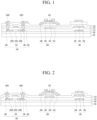
- FIG. 1 is a sectional view illustrating a substrate for a display device according to an embodiment.
- a substrate for a display device shown in FIG. 1 includes first and second thin-film transistors 100 and 150 and a storage capacitor 140.
- the first thin-film transistor 100 having a bottom gate configuration includes a first gate electrode 106, an oxide semiconductor layer 104, a first source electrode 108, and a first drain electrode 110.
- the first gate electrode 106 is formed on a first gate insulation film 112, and may overlap the oxide semiconductor layer 104 with first and second interlayer insulation films 114 and 116 and a second gate insulation film 152 interposed therebetween.
- the first gate electrode 106 is disposed on the first gate insulation film 112, on which a second gate electrode 156 is also disposed, and is formed of the same material as the second gate electrode 156. Accordingly, the first and second gate electrodes 106 and 156 may be formed through the same mask process, and therefore the number of mask processes may be reduced.
- the oxide semiconductor layer 104 is formed on the second gate insulation film 152 so as to overlap the first gate electrode 106, thereby forming a channel between the first source electrode 108 and the first drain electrode 110.
- the oxide semiconductor layer 104 is formed of oxide including at least one metal selected from among Zn, Cd, Ga, In, Sn, Hf, and Zr. Since the first thin-film transistor 100 including this oxide semiconductor layer 104 has advantages of higher electron mobility and lower off-current than the second thin-film transistor 150 including a polycrystalline semiconductor layer 154, it is suitable for application to a switching thin-film transistor, in which an On-time period is short but an Off-time period is long.
- the oxide semiconductor layer 104 may be disposed above the first gate electrode 106 so as to effectively ensure the stability of the device.
- the second gate insulation film 152 which has the same shape as the oxide semiconductor layer 104, is formed between the oxide semiconductor layer 104 and at least a first part of the second interlayer insulation film 116.
- the second gate insulation film 152 may contact the second interlayer insulation film 116.
- the second gate insulation film 152 is formed of a material having a selective etch ratio different from that of the first gate insulation film 112 and the first and second interlayer insulation films 114 and 116.
- the second gate insulation film 152 is formed of SiOx, which is an oxide film
- the first gate insulation film 112 and the first and second interlayer insulation films 114 and 116 are formed of SiNx, which is a nitride film.
- the second interlayer insulation film 116 which is exposed during a dry-etching process for forming the second gate insulation film 152 and the oxide semiconductor layer 104, from being damaged by a dry-etching gas used for the dry-etching process. Further, it is possible to prevent the second gate insulation film 152 and the oxide semiconductor layer 104, which are exposed during a dry-etching process for forming source and drain contact holes 164S and 164D that penetrate the first gate insulation film 112 and the first and second interlayer insulation films 114 and 116, from being damaged by a dry-etching gas used for the dry-etching process.
- the second gate insulation film 152 is an inorganic insulation film formed of, for example, silicon oxide (SiOx), which has lower hydrogen particle content than the first gate insulation film 112. Accordingly, it is possible to prevent hydrogen contained in the first gate insulation film 112 and hydrogen contained in the polycrystalline semiconductor layer 154 from being diffused to the oxide semiconductor layer 104 during a heat treatment process performed on the oxide semiconductor layer 104.
- SiOx silicon oxide
- Each of the first source electrode 108 and the first drain electrode 110 may be a single layer or multiple layers disposed on the second interlayer insulation film 116 and formed of any one selected from among molybdenum (Mo), aluminum (Al), chrome (Cr), gold (Au), titanium (Ti), nickel (Ni), neodymium (Nd), and copper (Cu), or an alloy thereof.
- Mo molybdenum
- Al aluminum
- Cr chrome
- Au gold
- Ti titanium
- Ni nickel
- Nd neodymium
- Cu copper
- the embodiment is not limited thereto.
- the first source electrode 108 and the first drain electrode 110 are formed to face each other with the channel of the oxide semiconductor layer 104 interposed therebetween. Meanwhile, an etch stopper (not shown) may be formed on the oxide semiconductor layer 104 that is exposed between the first source electrode 108 and the first drain electrode 110.
- the second thin-film transistor 150 having a top-gate configuration is disposed on a substrate 101 so as to be spaced apart from the first thin-film transistor 100.
- the second thin-film transistor 150 includes a polycrystalline semiconductor layer 154, a second gate electrode 156, a second source electrode 158, and a second drain electrode 160.
- the polycrystalline semiconductor layer 154 is formed on a buffer layer 102 that covers the substrate 101.
- the polycrystalline semiconductor layer 154 includes a channel region 154C, a source region 154S, and a drain region 154D.
- the channel region 154C overlaps the second gate electrode 156 with the first gate insulation film 112 interposed therebetween, and forms a channel between the second source electrode 158 and the second drain electrode 160.
- the source region 154S is electrically connected to the second source electrode 158 through a source contact hole 164S.
- the drain region 154D is electrically connected to the second drain electrode 160 through a drain contact hole 164D. Since the polycrystalline semiconductor layer 154 has high mobility, low power consumption, and high reliability, it is suitable for applications as a gate-driving unit for driving gate lines and/or to a multiplexer (MUX).
- MUX multiplexer
- the second gate electrode 156 overlaps the channel region 154C of the polycrystalline semiconductor layer with the first gate insulation film 112 interposed therebetween.
- the second gate electrode 156 has a smaller line width than the first gate electrode 106 and the intermediate storage electrode 144.
- the second gate electrode 156 may be a single layer or multiple layers formed of the same material as the first gate electrode 106, e.g. any one selected from among molybdenum (Mo), aluminum (Al), chrome (Cr), gold (Au), titanium (Ti), nickel (Ni), neodymium (Nd), and copper (Cu), or an alloy thereof.
- Mo molybdenum
- Al aluminum
- Cr chrome
- Au gold
- Ti titanium
- Ni nickel
- Nd neodymium
- Cu copper
- the embodiments are not limited thereto.
- the first gate insulation film 112 is positioned on the polycrystalline semiconductor layer 154, and is an inorganic insulation film formed of, for example, silicon nitride (SiNx), which has higher hydrogen particle content than the second gate insulation film 152.
- the hydrogen particles contained in the first gate insulation film 112 are diffused to the polycrystalline semiconductor layer 154 during a hydrogenation process, thereby enabling pores in the polycrystalline semiconductor layer 154 to be filled with hydrogen. Accordingly, the polycrystalline semiconductor layer 154 is stabilized, thus preventing deterioration of the properties of the second thin-film transistor 150.
- the second source electrode 158 is connected to the source region 154S of the polycrystalline semiconductor layer 154 through the source contact hole 164S that penetrates the first gate insulation film 112 and the first and second interlayer insulation films 114 and 116.
- the second drain electrode 160 faces the second source electrode 158, and is connected to the drain region 154D of the polycrystalline semiconductor layer 154 through the drain contact hole 164D that penetrates the first gate insulation film 112 and the first and second interlayer insulation films 114 and 116. Since the second source electrode 158 is in the same layer and is formed of the same material as the first source electrode 108, and since the second drain electrode 160 is in the same layer and is formed of the same material as the first drain electrode 110, the first and second source electrodes 108 and 158 and the first and second drain electrodes 110 and 160 may be formed at the same time through the same mask process.
- the oxide semiconductor layer 104 of the first thin-film transistor 100 is formed. That is, the oxide semiconductor layer 104 is disposed above the polycrystalline semiconductor layer 154. Accordingly, the oxide semiconductor layer 104 is not exposed to the high-temperature atmosphere of the activation and hydrogenation processes of the polycrystalline semiconductor layer 154, thereby preventing damage to the oxide semiconductor layer 104 and therefore improving reliability.
- the storage capacitor 140 includes a first storage capacitor and a second storage capacitor, which are connected in parallel.
- the first storage capacitor is formed such that a lower storage electrode 142 and an intermediate storage electrode 144 overlap each other with the first gate insulation film 112 interposed therebetween.
- the second storage capacitor is formed such that the intermediate storage electrode 144 and an upper storage electrode 146 overlap each other with at least one of the first and second interlayer insulation films 114 and 116 interposed therebetween.
- the lower storage electrode 142 is disposed on the buffer film 102, and is positioned in the same layer and is formed of the same material as the polycrystalline semiconductor layer 154.
- the intermediate storage electrode 144 is disposed on the first gate insulation film 112, and is positioned in the same layer and is formed of the same material as the second gate electrode 156.
- the upper storage electrode 146 is disposed on the second interlayer insulation film 116, and is positioned in the same layer and is formed of the same material as the source and drain electrodes 108, 158, 110, and 160.
- the first gate insulation film 112 and the first and second interlayer insulation films 114 and 116 are formed of an inorganic insulation material such as, for example, SiOx or SiNx.
- At least one of the first gate insulation film 112 and the first and second interlayer insulation films 114 and 116 may be formed of SiNx, which has a higher dielectric constant than SiOx. Accordingly, since the intermediate storage electrode 144 overlaps the lower storage electrode 142, with the first gate insulation film 112, which is formed of SiNx having a relatively high dielectric constant, interposed therebetween, the capacity of the first storage capacitor is increased in proportion to the dielectric constant. Similarly, since the upper storage electrode 146 overlaps the intermediate storage electrode 144 with the first and second interlayer insulation films 114 and 116, which are formed of SiNx having a relatively high dielectric constant, interposed therebetween, the capacity of the second storage capacitor is increased in proportion to the dielectric constant.
- the first and second interlayer insulation film 114 and 116 are interposed between the upper storage electrode 146 and the intermediate storage electrode 144.
- the second gate insulation film 152 over the intermediate storage electrode 144 is eliminated through etching process, and thus the upper storage electrode 146 is placed directly on the second interlayer insulation film 116.
- the upper storage electrode 146 does not contact the second gate insulation film 152, but contacts the second interlayer insulation film 116.
- the second interlayer insulation film 116 may be eliminated, and only the first interlayer insulation film 114, which is formed of SiNx, may be interposed between the upper storage electrode 146 and the intermediate storage electrode 144.
- the substrate for a display device having the above construction according to the present disclosure is applicable to the display device shown in FIG. 3 .
- the display device shown in FIG. 3 includes a display panel 180, a gate-driving unit 182 for driving gate lines GL of the display panel 180, and a data-driving unit 184 for driving data lines DL of the display panel 180.
- the display panel 180 includes a display area AA and a non-display area NA surrounding the display area AA.
- pixels are located at intersecting portions between the gate lines GL and the data lines DL.
- the pixels are arranged in a matrix form.
- Each of the pixels includes the storage capacitor 140 and at least one of the first thin-film transistor 100 and the second thin-film transistor 150.
- the gate-driving unit 182 is disposed in the non-display area NA.
- the gate-driving unit 182 is configured using the second thin-film transistor 150 including the polycrystalline semiconductor layer 154.
- the second thin-film transistor 150 of the gate-driving unit 182 is formed simultaneously with the first and second thin-film transistors 100 and 150 in the display area AA through the same process.
- the second thin-film transistor 150 of the multiplexer 186 may be directly formed on the substrate 101 for a display device together with the second thin-film transistor 150 of the gate-driving unit 182 and the first and second thin-film transistors 100 and 150 in the display area AA.
- the above-described display device is applicable to a display device that requires a thin-film transistor, e.g. the organic light-emitting display device shown in FIG. 4 or a liquid crystal display device.
- the organic light-emitting display device shown in FIG. 4 includes first and second thin-film transistors 100 and 150, a light-emitting diode 130 connected to the second thin-film transistor 150, and a storage capacitor 140.
- the first thin-film transistor 100 including an oxide semiconductor layer 104 is applied to a switching transistor of each pixel located in the display area AA
- the second thin-film transistor 150 including a polycrystalline semiconductor layer 154 is applied to a driving transistor of each pixel located in the display area AA
- the first thin-film transistor 100 including the oxide semiconductor layer 104 may be applied to a switching transistor for switching data voltage input to each pixel located in the display area AA and to a driving transistor connected to each light-emitting diode 130.
- the second thin-film transistor 150 including the polycrystalline semiconductor layer 154 is applied to a transistor of a driving circuit of at least one of the gate-driving unit 182 located in the non-display area NA and the multiplexer 186.
- the storage capacitor 140 includes a lower storage electrode 142, which is disposed on a buffer film 102, and an intermediate storage electrode 144, which overlaps the lower storage electrode 142 with a first gate insulation film 112 interposed therebetween.
- the lower storage electrode 142 is positioned in the same layer and is formed of the same material as the polycrystalline semiconductor layer 154, and the intermediate storage electrode 144 is positioned in the same layer and is formed of the same material as a second gate electrode 156. As shown in FIG.
- the intermediate storage electrode 144 is connected to a drain electrode 110 of any one of the switching transistor and the driving transistor through a first storage contact hole 148a, and the lower storage electrode 142 and the upper storage electrode 146 are connected to a drain electrode 160 of the remaining one of the switching transistor and the driving transistor through a second storage contact hole 148b.
- the light-emitting diode 130 is a light-emitting device, and includes an anode 132, which is connected to the second drain electrode 160 of the second thin-film transistor 150, at least one light-emitting stack 134, which is formed on the anode 132, and a cathode 136, which is formed on the light-emitting stack 134.
- the anode 132 is connected to a pixel connection electrode 124, which is exposed through a second pixel contact hole 120 that penetrates a planarization layer 128.
- the pixel connection electrode 124 is connected to the second drain electrode 160, which is exposed through a first pixel contact hole 122 that penetrates first and second protective films 118 and 126.
- the anode 132 is formed in a multilayer structure including a transparent conductive film and an opaque conductive film having high reflection efficiency.
- the transparent conductive film is formed of a material having a relatively high work function, e.g.
- the opaque conductive film is formed in a single-layer or multilayer structure including any one selected from among Al, Ag, Cu, Pb, Mo, and Ti or an alloy thereof.
- the anode 132 may be formed in a structure such that a transparent conductive film, an opaque conductive film and a transparent conductive film are sequentially stacked, or such that a transparent conductive film and an opaque conductive film are sequentially stacked.
- the polycrystalline semiconductor layer 154 and the lower storage electrode 142 are formed by patterning the polycrystalline silicon thin film through a photolithography process using a first mask and an etching process. Subsequently, the lower storage electrode 142, excluding the polycrystalline semiconductor layer 154, is selectively doped with impurities through a photolithography process using a second mask, thereby forming the lower storage electrode 142 having conductivity.
- the first and second protective films 118 and 126 are sequentially formed on the substrate 101, on which the first and second source electrodes 108 and 158, the first and second drain electrodes 110 and 160 and the upper storage electrode 146 have been formed, through a deposition process.
- the first and second protective films 118 and 126 are formed of an inorganic insulation material such as SiOx or SiNx or an organic insulation material such as an acrylic resin.
- the first and second protective films 118 and 126 are patterned through a photolithography process using a seventh mask and an etching process, thereby forming the first pixel contact hole 122.
Landscapes
- Engineering & Computer Science (AREA)
- Microelectronics & Electronic Packaging (AREA)
- Physics & Mathematics (AREA)
- Geometry (AREA)
- Computer Hardware Design (AREA)
- General Physics & Mathematics (AREA)
- Theoretical Computer Science (AREA)
- Devices For Indicating Variable Information By Combining Individual Elements (AREA)
- Electroluminescent Light Sources (AREA)
- Chemical & Material Sciences (AREA)
- Crystallography & Structural Chemistry (AREA)
- Thin Film Transistor (AREA)
Applications Claiming Priority (2)
| Application Number | Priority Date | Filing Date | Title |
|---|---|---|---|
| KR1020160174261A KR20180071538A (ko) | 2016-12-20 | 2016-12-20 | 표시 장치용 기판과 그를 포함하는 표시 장치 |
| EP17208677.9A EP3340301B1 (de) | 2016-12-20 | 2017-12-19 | Substrat für eine anzeigevorrichtung und anzeigevorrichtung damit |
Related Parent Applications (1)
| Application Number | Title | Priority Date | Filing Date |
|---|---|---|---|
| EP17208677.9A Division EP3340301B1 (de) | 2016-12-20 | 2017-12-19 | Substrat für eine anzeigevorrichtung und anzeigevorrichtung damit |
Publications (2)
| Publication Number | Publication Date |
|---|---|
| EP4398301A2 true EP4398301A2 (de) | 2024-07-10 |
| EP4398301A3 EP4398301A3 (de) | 2024-09-25 |
Family
ID=60937551
Family Applications (2)
| Application Number | Title | Priority Date | Filing Date |
|---|---|---|---|
| EP24178116.0A Pending EP4398301A3 (de) | 2016-12-20 | 2017-12-19 | Substrat für eine anzeigevorrichtung und anzeigevorrichtung damit |
| EP17208677.9A Active EP3340301B1 (de) | 2016-12-20 | 2017-12-19 | Substrat für eine anzeigevorrichtung und anzeigevorrichtung damit |
Family Applications After (1)
| Application Number | Title | Priority Date | Filing Date |
|---|---|---|---|
| EP17208677.9A Active EP3340301B1 (de) | 2016-12-20 | 2017-12-19 | Substrat für eine anzeigevorrichtung und anzeigevorrichtung damit |
Country Status (4)
| Country | Link |
|---|---|
| US (2) | US10340320B2 (de) |
| EP (2) | EP4398301A3 (de) |
| KR (1) | KR20180071538A (de) |
| CN (2) | CN114664865B (de) |
Families Citing this family (36)
| Publication number | Priority date | Publication date | Assignee | Title |
|---|---|---|---|---|
| KR102109166B1 (ko) | 2013-01-15 | 2020-05-12 | 삼성디스플레이 주식회사 | 박막 트랜지스터 및 이를 구비하는 표시 기판 |
| KR20180071538A (ko) * | 2016-12-20 | 2018-06-28 | 엘지디스플레이 주식회사 | 표시 장치용 기판과 그를 포함하는 표시 장치 |
| KR102873477B1 (ko) * | 2016-12-28 | 2025-10-20 | 엘지디스플레이 주식회사 | 표시 장치용 기판과 그를 포함하는 표시 장치 |
| KR102465376B1 (ko) * | 2017-06-16 | 2022-11-10 | 삼성디스플레이 주식회사 | 표시 장치 및 표시 장치의 제조 방법 |
| KR102173434B1 (ko) * | 2017-12-19 | 2020-11-03 | 엘지디스플레이 주식회사 | 표시 장치 |
| CN108288621B (zh) * | 2018-03-09 | 2021-01-26 | 京东方科技集团股份有限公司 | 阵列基板的制造方法、阵列基板及显示面板 |
| WO2019186924A1 (ja) * | 2018-03-29 | 2019-10-03 | シャープ株式会社 | 表示装置及び表示装置の製造方法 |
| CN109065590B (zh) | 2018-08-09 | 2020-12-04 | 京东方科技集团股份有限公司 | 有机发光显示基板及其制作方法、有机发光显示装置 |
| KR102469187B1 (ko) * | 2018-09-04 | 2022-11-21 | 삼성디스플레이 주식회사 | 표시 장치 및 그 제조 방법 |
| US10910413B2 (en) * | 2018-10-10 | 2021-02-02 | HKC Corporation Limited | Method of manufacturing array substrate and array substrate |
| KR102711213B1 (ko) * | 2018-10-15 | 2024-09-27 | 엘지디스플레이 주식회사 | 디스플레이 패널 및 디스플레이 장치 |
| JP6753450B2 (ja) * | 2018-11-12 | 2020-09-09 | セイコーエプソン株式会社 | 電気光学装置用基板、電気光学装置、電子機器 |
| KR102701984B1 (ko) | 2018-12-26 | 2024-09-02 | 엘지디스플레이 주식회사 | 서로 다른 타입의 박막 트랜지스터들을 포함하는 표시장치 및 그 제조방법 |
| KR102690931B1 (ko) | 2019-01-17 | 2024-08-01 | 삼성디스플레이 주식회사 | 표시 장치와 그의 제조 방법 |
| WO2020210946A1 (en) * | 2019-04-15 | 2020-10-22 | Boe Technology Group Co., Ltd. | Method of fabricating array substrate, array substrate, and display apparatus |
| WO2020231398A1 (en) * | 2019-05-13 | 2020-11-19 | Hewlett-Packard Development Company, L.P. | Thin-film transistors |
| KR102812018B1 (ko) * | 2019-08-26 | 2025-05-23 | 엘지디스플레이 주식회사 | 표시 패널 및 이를 포함한 헤드 장착형 표시 장치 |
| CN110556386A (zh) * | 2019-09-05 | 2019-12-10 | 京东方科技集团股份有限公司 | 驱动背板及其制备方法、显示面板 |
| KR102853446B1 (ko) | 2019-10-11 | 2025-09-02 | 삼성디스플레이 주식회사 | 표시 장치와 그의 제조 방법 |
| KR102825654B1 (ko) * | 2019-12-24 | 2025-06-26 | 엘지디스플레이 주식회사 | 표시 장치 |
| CN111834400B (zh) * | 2020-02-26 | 2021-10-12 | 昆山国显光电有限公司 | 显示面板及其制造方法、显示装置 |
| KR102867626B1 (ko) * | 2020-03-18 | 2025-10-02 | 삼성디스플레이 주식회사 | 표시 장치 및 표시 장치의 제조 방법 |
| CN111384070B (zh) * | 2020-03-25 | 2023-05-19 | 京东方科技集团股份有限公司 | 一种像素结构、阵列基板、显示装置和制作方法 |
| US20220140048A1 (en) * | 2020-03-31 | 2022-05-05 | Boe Technology Group Co., Ltd. | Display panel, method for preparing the same, and display device |
| CN111933681A (zh) * | 2020-09-07 | 2020-11-13 | 深圳市华星光电半导体显示技术有限公司 | 顶发光amoled显示面板、制作方法以及显示装置 |
| KR20220034280A (ko) * | 2020-09-10 | 2022-03-18 | 삼성디스플레이 주식회사 | 표시 장치 및 이의 제조 방법 |
| CN112670247B (zh) * | 2020-12-23 | 2024-02-02 | 武汉天马微电子有限公司 | 一种显示面板的制备方法、显示面板及显示装置 |
| KR102804064B1 (ko) * | 2020-12-29 | 2025-05-09 | 엘지디스플레이 주식회사 | 표시패널 및 그 제조 방법 |
| KR20220097675A (ko) | 2020-12-30 | 2022-07-08 | 삼성디스플레이 주식회사 | 표시 장치 |
| CN119997607A (zh) * | 2020-12-30 | 2025-05-13 | 厦门天马微电子有限公司 | 显示面板及显示装置 |
| US12396329B2 (en) * | 2021-03-26 | 2025-08-19 | Samsung Display Co., Ltd. | Display apparatus |
| KR20230119822A (ko) * | 2022-02-08 | 2023-08-16 | 엘지디스플레이 주식회사 | 유기 발광 표시 장치 및 그 제조 방법 |
| US20240324372A1 (en) * | 2022-04-19 | 2024-09-26 | Beijing Boe Technology Development Co., Ltd. | Display Substrate and Display Apparatus |
| EP4459604A4 (de) * | 2022-06-30 | 2025-04-02 | Boe Technology Group Co., Ltd. | Anzeigetafel und anzeigevorrichtung |
| TWI802478B (zh) * | 2022-07-27 | 2023-05-11 | 友達光電股份有限公司 | 主動元件基板 |
| KR20260025965A (ko) * | 2024-08-16 | 2026-02-25 | 삼성디스플레이 주식회사 | 표시 장치 및 이의 제조 방법 |
Family Cites Families (22)
| Publication number | Priority date | Publication date | Assignee | Title |
|---|---|---|---|---|
| DE69942442D1 (de) * | 1999-01-11 | 2010-07-15 | Semiconductor Energy Lab | Halbleiteranordnung mit Treiber-TFT und Pixel-TFT auf einem Substrat |
| KR100726132B1 (ko) * | 2000-10-31 | 2007-06-12 | 엘지.필립스 엘시디 주식회사 | 액정표시장치용 어레이기판과 그 제조방법 |
| KR101074788B1 (ko) * | 2009-01-30 | 2011-10-20 | 삼성모바일디스플레이주식회사 | 평판 표시 장치 및 이의 제조 방법 |
| TWI535023B (zh) * | 2009-04-16 | 2016-05-21 | 半導體能源研究所股份有限公司 | 半導體裝置和其製造方法 |
| WO2011007675A1 (en) * | 2009-07-17 | 2011-01-20 | Semiconductor Energy Laboratory Co., Ltd. | Semiconductor device and manufacturing method thereof |
| JP5253674B2 (ja) * | 2010-08-30 | 2013-07-31 | シャープ株式会社 | 半導体装置およびその製造方法 |
| KR101781532B1 (ko) | 2011-03-14 | 2017-10-24 | 삼성디스플레이 주식회사 | 유기 발광 표시 장치와 그 제조방법 |
| TWI453516B (zh) | 2011-07-13 | 2014-09-21 | 友達光電股份有限公司 | 畫素結構及其製作方法 |
| KR102072244B1 (ko) * | 2011-11-30 | 2020-01-31 | 가부시키가이샤 한도오따이 에네루기 켄큐쇼 | 반도체 장치 및 반도체 장치의 제작 방법 |
| KR101901832B1 (ko) * | 2011-12-14 | 2018-09-28 | 삼성디스플레이 주식회사 | 유기 발광 표시 장치 및 유기 발광 표시 장치의 제조 방법 |
| US9929276B2 (en) * | 2012-08-10 | 2018-03-27 | Semiconductor Energy Laboratory Co., Ltd. | Semiconductor device and method for manufacturing the same |
| KR102109166B1 (ko) * | 2013-01-15 | 2020-05-12 | 삼성디스플레이 주식회사 | 박막 트랜지스터 및 이를 구비하는 표시 기판 |
| KR102077143B1 (ko) * | 2013-05-30 | 2020-02-14 | 삼성디스플레이 주식회사 | 유기 발광 표시 장치 및 그 제조 방법 |
| US9818765B2 (en) * | 2013-08-26 | 2017-11-14 | Apple Inc. | Displays with silicon and semiconducting oxide thin-film transistors |
| US10325937B2 (en) * | 2014-02-24 | 2019-06-18 | Lg Display Co., Ltd. | Thin film transistor substrate with intermediate insulating layer and display using the same |
| CN105390504B (zh) * | 2014-08-29 | 2019-02-01 | 乐金显示有限公司 | 薄膜晶体管基板及使用它的显示装置 |
| US9543370B2 (en) * | 2014-09-24 | 2017-01-10 | Apple Inc. | Silicon and semiconducting oxide thin-film transistor displays |
| KR102226236B1 (ko) * | 2014-10-13 | 2021-03-11 | 엘지디스플레이 주식회사 | 유기 발광 표시 장치 |
| US10020354B2 (en) * | 2015-04-17 | 2018-07-10 | Apple Inc. | Organic light-emitting diode displays with silicon and semiconducting oxide thin-film transistors |
| CN105929615B (zh) * | 2016-06-21 | 2019-05-03 | 武汉华星光电技术有限公司 | 一种薄膜晶体管阵列基板及液晶面板 |
| US9985082B2 (en) * | 2016-07-06 | 2018-05-29 | Lg Display Co., Ltd. | Organic light emitting display device comprising multi-type thin film transistor and method of manufacturing the same |
| KR20180071538A (ko) * | 2016-12-20 | 2018-06-28 | 엘지디스플레이 주식회사 | 표시 장치용 기판과 그를 포함하는 표시 장치 |
-
2016
- 2016-12-20 KR KR1020160174261A patent/KR20180071538A/ko active Pending
-
2017
- 2017-11-10 US US15/809,946 patent/US10340320B2/en active Active
- 2017-11-28 CN CN202210153249.0A patent/CN114664865B/zh active Active
- 2017-11-28 CN CN201711215133.0A patent/CN108206192B/zh active Active
- 2017-12-19 EP EP24178116.0A patent/EP4398301A3/de active Pending
- 2017-12-19 EP EP17208677.9A patent/EP3340301B1/de active Active
-
2019
- 2019-05-10 US US16/409,718 patent/US10714557B2/en active Active
Also Published As
| Publication number | Publication date |
|---|---|
| CN108206192A (zh) | 2018-06-26 |
| EP3340301A1 (de) | 2018-06-27 |
| US20180175127A1 (en) | 2018-06-21 |
| EP3340301B1 (de) | 2024-06-12 |
| EP4398301A3 (de) | 2024-09-25 |
| US10340320B2 (en) | 2019-07-02 |
| CN108206192B (zh) | 2022-03-11 |
| US10714557B2 (en) | 2020-07-14 |
| CN114664865A (zh) | 2022-06-24 |
| KR20180071538A (ko) | 2018-06-28 |
| CN114664865B (zh) | 2026-03-17 |
| US20190267441A1 (en) | 2019-08-29 |
Similar Documents
| Publication | Publication Date | Title |
|---|---|---|
| US10714557B2 (en) | Substrate for display device and display device including the same | |
| US10692893B2 (en) | Substrate for display device and display device including the same | |
| US11765937B2 (en) | Display device | |
| US11063068B2 (en) | Display apparatus | |
| US11158700B2 (en) | Display device having multiple buffer layers | |
| US10937816B2 (en) | Switching element, manufacturing method thereof, array substrate and display device | |
| KR102457204B1 (ko) | 박막 트랜지스터 기판 및 이를 이용한 표시장치 | |
| JP2017120893A (ja) | 薄膜トランジスタ基板 | |
| KR102468858B1 (ko) | 표시 장치용 기판과 그를 포함하는 표시 장치 | |
| KR20120053768A (ko) | 유기전계발광표시장치 및 그 제조방법 | |
| KR102585853B1 (ko) | 표시 장치용 기판과 그를 포함하는 표시 장치 | |
| KR102220681B1 (ko) | 유기전계 발광소자 광원을 구비한 표시장치 | |
| KR102501143B1 (ko) | 표시 장치의 제조방법 | |
| KR102871406B1 (ko) | 표시 장치 및 표시 장치의 제조 방법 | |
| KR20200020327A (ko) | 표시 장치용 기판과 그를 포함하는 표시 장치 |
Legal Events
| Date | Code | Title | Description |
|---|---|---|---|
| PUAI | Public reference made under article 153(3) epc to a published international application that has entered the european phase |
Free format text: ORIGINAL CODE: 0009012 |
|
| STAA | Information on the status of an ep patent application or granted ep patent |
Free format text: STATUS: REQUEST FOR EXAMINATION WAS MADE |
|
| 17P | Request for examination filed |
Effective date: 20240525 |
|
| AC | Divisional application: reference to earlier application |
Ref document number: 3340301 Country of ref document: EP Kind code of ref document: P |
|
| AK | Designated contracting states |
Kind code of ref document: A2 Designated state(s): AL AT BE BG CH CY CZ DE DK EE ES FI FR GB GR HR HU IE IS IT LI LT LU LV MC MK MT NL NO PL PT RO RS SE SI SK SM TR |
|
| REG | Reference to a national code |
Ref country code: DE Ref legal event code: R079 Free format text: PREVIOUS MAIN CLASS: H01L0027120000 Ipc: H10K0059121000 |
|
| PUAL | Search report despatched |
Free format text: ORIGINAL CODE: 0009013 |
|
| AK | Designated contracting states |
Kind code of ref document: A3 Designated state(s): AL AT BE BG CH CY CZ DE DK EE ES FI FR GB GR HR HU IE IS IT LI LT LU LV MC MK MT NL NO PL PT RO RS SE SI SK SM TR |
|
| RIC1 | Information provided on ipc code assigned before grant |
Ipc: H01L 27/12 20060101ALI20240821BHEP Ipc: H10K 59/121 20230101AFI20240821BHEP |
|
| RBV | Designated contracting states (corrected) |
Designated state(s): AL AT BE BG CH CY CZ DE DK EE ES FI FR GB GR HR HU IE IS IT LI LT LU LV MC MK MT NL NO PL PT RO RS SE SI SK SM TR |
|
| STAA | Information on the status of an ep patent application or granted ep patent |
Free format text: STATUS: EXAMINATION IS IN PROGRESS |