EP4398291A1 - Wiring substrate and electronic device - Google Patents
Wiring substrate and electronic device Download PDFInfo
- Publication number
- EP4398291A1 EP4398291A1 EP22864341.7A EP22864341A EP4398291A1 EP 4398291 A1 EP4398291 A1 EP 4398291A1 EP 22864341 A EP22864341 A EP 22864341A EP 4398291 A1 EP4398291 A1 EP 4398291A1
- Authority
- EP
- European Patent Office
- Prior art keywords
- heat dissipation
- dissipation member
- frame
- metal layer
- shaped metal
- Prior art date
- Legal status (The legal status is an assumption and is not a legal conclusion. Google has not performed a legal analysis and makes no representation as to the accuracy of the status listed.)
- Pending
Links
Images








Classifications
-
- H—ELECTRICITY
- H10—SEMICONDUCTOR DEVICES; ELECTRIC SOLID-STATE DEVICES NOT OTHERWISE PROVIDED FOR
- H10H—INORGANIC LIGHT-EMITTING SEMICONDUCTOR DEVICES HAVING POTENTIAL BARRIERS
- H10H20/00—Individual inorganic light-emitting semiconductor devices having potential barriers, e.g. light-emitting diodes [LED]
- H10H20/80—Constructional details
- H10H20/85—Packages
- H10H20/858—Means for heat extraction or cooling
-
- H—ELECTRICITY
- H05—ELECTRIC TECHNIQUES NOT OTHERWISE PROVIDED FOR
- H05K—PRINTED CIRCUITS; CASINGS OR CONSTRUCTIONAL DETAILS OF ELECTRIC APPARATUS; MANUFACTURE OF ASSEMBLAGES OF ELECTRICAL COMPONENTS
- H05K1/00—Printed circuits
- H05K1/02—Details
-
- H—ELECTRICITY
- H10—SEMICONDUCTOR DEVICES; ELECTRIC SOLID-STATE DEVICES NOT OTHERWISE PROVIDED FOR
- H10H—INORGANIC LIGHT-EMITTING SEMICONDUCTOR DEVICES HAVING POTENTIAL BARRIERS
- H10H20/00—Individual inorganic light-emitting semiconductor devices having potential barriers, e.g. light-emitting diodes [LED]
- H10H20/80—Constructional details
- H10H20/85—Packages
- H10H20/8502—Surface mount technology [SMT] type packages
-
- H—ELECTRICITY
- H10—SEMICONDUCTOR DEVICES; ELECTRIC SOLID-STATE DEVICES NOT OTHERWISE PROVIDED FOR
- H10H—INORGANIC LIGHT-EMITTING SEMICONDUCTOR DEVICES HAVING POTENTIAL BARRIERS
- H10H20/00—Individual inorganic light-emitting semiconductor devices having potential barriers, e.g. light-emitting diodes [LED]
- H10H20/80—Constructional details
- H10H20/85—Packages
- H10H20/8506—Containers
-
- H—ELECTRICITY
- H10—SEMICONDUCTOR DEVICES; ELECTRIC SOLID-STATE DEVICES NOT OTHERWISE PROVIDED FOR
- H10H—INORGANIC LIGHT-EMITTING SEMICONDUCTOR DEVICES HAVING POTENTIAL BARRIERS
- H10H20/00—Individual inorganic light-emitting semiconductor devices having potential barriers, e.g. light-emitting diodes [LED]
- H10H20/80—Constructional details
- H10H20/85—Packages
- H10H20/8508—Package substrates, e.g. submounts
-
- H—ELECTRICITY
- H10—SEMICONDUCTOR DEVICES; ELECTRIC SOLID-STATE DEVICES NOT OTHERWISE PROVIDED FOR
- H10H—INORGANIC LIGHT-EMITTING SEMICONDUCTOR DEVICES HAVING POTENTIAL BARRIERS
- H10H20/00—Individual inorganic light-emitting semiconductor devices having potential barriers, e.g. light-emitting diodes [LED]
- H10H20/80—Constructional details
- H10H20/85—Packages
- H10H20/855—Optical field-shaping means, e.g. lenses
-
- H—ELECTRICITY
- H10—SEMICONDUCTOR DEVICES; ELECTRIC SOLID-STATE DEVICES NOT OTHERWISE PROVIDED FOR
- H10H—INORGANIC LIGHT-EMITTING SEMICONDUCTOR DEVICES HAVING POTENTIAL BARRIERS
- H10H20/00—Individual inorganic light-emitting semiconductor devices having potential barriers, e.g. light-emitting diodes [LED]
- H10H20/80—Constructional details
- H10H20/85—Packages
- H10H20/857—Interconnections, e.g. lead-frames, bond wires or solder balls
-
- H—ELECTRICITY
- H10—SEMICONDUCTOR DEVICES; ELECTRIC SOLID-STATE DEVICES NOT OTHERWISE PROVIDED FOR
- H10H—INORGANIC LIGHT-EMITTING SEMICONDUCTOR DEVICES HAVING POTENTIAL BARRIERS
- H10H20/00—Individual inorganic light-emitting semiconductor devices having potential barriers, e.g. light-emitting diodes [LED]
- H10H20/80—Constructional details
- H10H20/85—Packages
- H10H20/858—Means for heat extraction or cooling
- H10H20/8582—Means for heat extraction or cooling characterised by their shape
-
- H—ELECTRICITY
- H10—SEMICONDUCTOR DEVICES; ELECTRIC SOLID-STATE DEVICES NOT OTHERWISE PROVIDED FOR
- H10W—GENERIC PACKAGES, INTERCONNECTIONS, CONNECTORS OR OTHER CONSTRUCTIONAL DETAILS OF DEVICES COVERED BY CLASS H10
- H10W40/00—Arrangements for thermal protection or thermal control
- H10W40/20—Arrangements for cooling
- H10W40/22—Arrangements for cooling characterised by their shape, e.g. having conical or cylindrical projections
- H10W40/226—Arrangements for cooling characterised by their shape, e.g. having conical or cylindrical projections characterised by projecting parts, e.g. fins to increase surface area
- H10W40/228—Arrangements for cooling characterised by their shape, e.g. having conical or cylindrical projections characterised by projecting parts, e.g. fins to increase surface area the projecting parts being wire-shaped or pin-shaped
-
- H—ELECTRICITY
- H10—SEMICONDUCTOR DEVICES; ELECTRIC SOLID-STATE DEVICES NOT OTHERWISE PROVIDED FOR
- H10W—GENERIC PACKAGES, INTERCONNECTIONS, CONNECTORS OR OTHER CONSTRUCTIONAL DETAILS OF DEVICES COVERED BY CLASS H10
- H10W70/00—Package substrates; Interposers; Redistribution layers [RDL]
- H10W70/60—Insulating or insulated package substrates; Interposers; Redistribution layers
-
- H—ELECTRICITY
- H10—SEMICONDUCTOR DEVICES; ELECTRIC SOLID-STATE DEVICES NOT OTHERWISE PROVIDED FOR
- H10W—GENERIC PACKAGES, INTERCONNECTIONS, CONNECTORS OR OTHER CONSTRUCTIONAL DETAILS OF DEVICES COVERED BY CLASS H10
- H10W70/00—Package substrates; Interposers; Redistribution layers [RDL]
- H10W70/60—Insulating or insulated package substrates; Interposers; Redistribution layers
- H10W70/67—Insulating or insulated package substrates; Interposers; Redistribution layers characterised by their insulating layers or insulating parts
- H10W70/68—Shapes or dispositions thereof
Definitions
- the present disclosure relates to a wiring substrate and an electronic device.
- a bonding material may flow to a component mounting surface side of the heat dissipation member.
- the flatness of the component mounting surface of the heat dissipation member deteriorates.
- the flatness of the component mounting surface of the heat dissipation member can be improved.
- dots are applied to a surface of a conductor portion, a surface of an electronic component, a surface of a heat dissipation member, and a surface of a brazing material.
- FIG. 1 is a schematic perspective view of an electronic device according to a first embodiment, illustrating a state in which a lid is removed.
- FIG. 2 is a schematic plan view of the electronic device illustrated in FIG. 1 .
- FIG. 3 is a schematic bottom view of the electronic device illustrated in FIG. 1 .
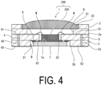
- FIG. 4 is a schematic cross-sectional view of the electronic device illustrated in FIG. 1 .
- FIG. 5 is a schematic perspective view of a wiring substrate according to the first embodiment as viewed from an insulating frame body side.
- FIG. 6 is a schematic perspective view of the wiring substrate illustrated in FIG. 5 as viewed from a second surface side of an insulating substrate.
- FIG. 7 is a schematic perspective view of the wiring substrate illustrated in FIG. 5 as viewed from the second surface side of the insulating substrate, illustrating a state in which a heat dissipation member is removed.
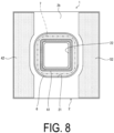
- FIG. 8 is a schematic bottom view of the wiring substrate illustrated in FIG. 5 , illustrating a state in which the heat dissipation member is removed.
- FIG. 9 is a schematic cross-sectional view illustrating a state in which the electronic device illustrated in FIG. 1 is mounted on a mother substrate.
- an electronic device 200 according to the first embodiment includes a wiring substrate 1 according to the first embodiment and an electronic component 300 mounted on the wiring substrate 1.
- the wiring substrate 1 according to the first embodiment includes an insulating substrate 2.
- the insulating substrate 2 is made of, for example, a ceramic such as an aluminum oxide-based sintered body (alumina ceramic), an aluminum nitride-based sintered body, a mullite-based sintered body, or a glass ceramic sintered body.
- the insulating substrate 2 is composed of a plurality of insulating layers.
- the insulating substrate 2 has a first surface 2a, a second surface 2b located on an opposite side to the first surface 2a, a recessed portion 21 opening to the second surface 2b, and a rectangular through hole 22 penetrating from a bottom surface of the recessed portion 21 to the first surface 2a.
- the recessed portion 21 of the insulating substrate 2 has a rectangular shape in a bottom view, and the size of the recessed portion 21 of the insulating substrate 2 is larger than the size of the through hole 22 of the insulating substrate 2.
- the through hole 22 of the insulating substrate 2 has a rectangular shape in a plan view, and is a hole for accommodating the electronic component 300.
- An inner peripheral surface of the recessed portion 21 of the insulating substrate 2 and an inner peripheral surface of the through hole 22 are parallel in a thickness direction of the insulating substrate 2, respectively.
- a shape of the recessed portion 21 of the insulating substrate 2 in a bottom view and a shape of the through hole 22 in a plan view are not limited to the rectangular shape, and may be each a shape other than the rectangular shape, such as a circular shape.
- the electronic device 200A may include the cap-shaped lid 8A.
- the lid 8A has a cap-shaped lid main body 81A bonded to the metalized layer 10, and the lid main body 81A is made of, for example, metal having a small difference in thermal expansion coefficient from a ceramic such as an iron-nickel (Fe-Ni) alloy or an iron-nickel-cobalt (Fe-Ni-Co) alloy.
- the lid main body 81A may also be made of a ceramic other than metal.
- the lid main body 81A can be produced by pressing a metal plate.
- the lid main body 81A is made of a ceramic, a laminate of ceramic green sheets may be fired in the same manner as the insulating substrate 2, or ceramic powder may be press-molded into a cap shape and then fired.
- FIG. 17 is a schematic cross-sectional view taken along a line XVII-XVII in FIG. 19 .
- FIG. 18 is a schematic cross-sectional view taken along a line XVIII-XVIII in FIG. 19.
- FIG. 19 is a schematic bottom view of an electronic device according to a third embodiment.
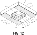
- FIG. 20 is a schematic perspective view of a wiring substrate according to the third embodiment as viewed from a second surface side of an insulating substrate, illustrating a state in which a heat dissipation member is removed.
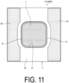
- FIG. 21 is a schematic bottom view of the wiring substrate illustrated in FIG. 20 , illustrating a state in which the heat dissipation member is removed.
- FIG. 21 is a schematic bottom view of the wiring substrate illustrated in FIG. 20 , illustrating a state in which the heat dissipation member is removed.
Landscapes
- Engineering & Computer Science (AREA)
- Microelectronics & Electronic Packaging (AREA)
- Structure Of Printed Boards (AREA)
- Insulated Metal Substrates For Printed Circuits (AREA)
Applications Claiming Priority (2)
| Application Number | Priority Date | Filing Date | Title |
|---|---|---|---|
| JP2021141686 | 2021-08-31 | ||
| PCT/JP2022/031717 WO2023032757A1 (ja) | 2021-08-31 | 2022-08-23 | 配線基板および電子装置 |
Publications (1)
| Publication Number | Publication Date |
|---|---|
| EP4398291A1 true EP4398291A1 (en) | 2024-07-10 |
Family
ID=85412253
Family Applications (1)
| Application Number | Title | Priority Date | Filing Date |
|---|---|---|---|
| EP22864341.7A Pending EP4398291A1 (en) | 2021-08-31 | 2022-08-23 | Wiring substrate and electronic device |
Country Status (5)
| Country | Link |
|---|---|
| EP (1) | EP4398291A1 (https=) |
| JP (1) | JP7679479B2 (https=) |
| CN (1) | CN117836926A (https=) |
| TW (1) | TWI869699B (https=) |
| WO (1) | WO2023032757A1 (https=) |
Family Cites Families (16)
| Publication number | Priority date | Publication date | Assignee | Title |
|---|---|---|---|---|
| JPS63106143U (https=) * | 1986-12-26 | 1988-07-08 | ||
| JP2605865Y2 (ja) * | 1992-05-29 | 2000-08-21 | 京セラ株式会社 | Ccd素子収納用パッケージ |
| JP3391117B2 (ja) * | 1994-11-02 | 2003-03-31 | 富士通株式会社 | 光デバイスの製造方法 |
| TW456004B (en) * | 1998-02-10 | 2001-09-21 | Nissha Printing | Substrate sheet for semiconductor module, method and apparatus for manufacturing the same |
| JP2000188356A (ja) * | 1998-12-24 | 2000-07-04 | Ngk Spark Plug Co Ltd | 配線基板及びその製造方法 |
| JP2006093565A (ja) * | 2004-09-27 | 2006-04-06 | Kyocera Corp | 発光素子用配線基板ならびに発光装置およびその製造方法 |
| US20080043444A1 (en) * | 2004-04-27 | 2008-02-21 | Kyocera Corporation | Wiring Board for Light-Emitting Element |
| JP2006128511A (ja) * | 2004-10-29 | 2006-05-18 | Ngk Spark Plug Co Ltd | 発光素子用セラミック基板 |
| JP2007234846A (ja) * | 2006-03-01 | 2007-09-13 | Ngk Spark Plug Co Ltd | 発光素子用セラミックパッケージ |
| JP4789671B2 (ja) * | 2006-03-28 | 2011-10-12 | 京セラ株式会社 | 発光素子用配線基板ならびに発光装置 |
| JP2007311445A (ja) * | 2006-05-17 | 2007-11-29 | Stanley Electric Co Ltd | 半導体発光装置及びその製造方法 |
| JP5393419B2 (ja) * | 2009-11-27 | 2014-01-22 | 京セラ株式会社 | 発光素子搭載用基板および発光装置 |
| TW201312807A (zh) * | 2011-07-21 | 2013-03-16 | 克里股份有限公司 | 光發射器元件封裝與部件及改良化學抵抗性的方法與相關方法 |
| JP6400985B2 (ja) * | 2014-08-28 | 2018-10-03 | 京セラ株式会社 | 電子素子実装用基板及び電子装置 |
| US11582858B2 (en) * | 2018-08-29 | 2023-02-14 | Kyocera Corporation | Wiring substrate, electronic device and electronic module |
| WO2020175619A1 (ja) * | 2019-02-28 | 2020-09-03 | 京セラ株式会社 | 電子部品搭載用パッケージ、電子装置及び発光装置 |
-
2022
- 2022-08-23 JP JP2023545477A patent/JP7679479B2/ja active Active
- 2022-08-23 CN CN202280057177.8A patent/CN117836926A/zh active Pending
- 2022-08-23 EP EP22864341.7A patent/EP4398291A1/en active Pending
- 2022-08-23 WO PCT/JP2022/031717 patent/WO2023032757A1/ja not_active Ceased
- 2022-08-25 TW TW111132050A patent/TWI869699B/zh active
Also Published As
| Publication number | Publication date |
|---|---|
| JP7679479B2 (ja) | 2025-05-19 |
| CN117836926A (zh) | 2024-04-05 |
| TW202316587A (zh) | 2023-04-16 |
| WO2023032757A1 (ja) | 2023-03-09 |
| JPWO2023032757A1 (https=) | 2023-03-09 |
| TWI869699B (zh) | 2025-01-11 |
Similar Documents
| Publication | Publication Date | Title |
|---|---|---|
| JP6483800B2 (ja) | 発光素子搭載用パッケージ、発光装置および発光モジュール | |
| CN103180941B (zh) | 布线基板 | |
| US11315844B2 (en) | Electronic device mounting board, electronic package, and electronic module | |
| CN107534268A (zh) | 光元件搭载用封装件、电子装置以及电子模块 | |
| US10334740B2 (en) | Electronic-component mount substrate, electronic device, and electronic module | |
| CN111727513B (zh) | 电子部件搭载用封装件、电子装置以及电子模块 | |
| EP3136430B1 (en) | Wiring board, electronic device, and electronic module | |
| CN104412722B (zh) | 布线基板、电子装置以及发光装置 | |
| US20060125076A1 (en) | Circuit boards, electronic devices, and methods of manufacturing thereof | |
| CN119133136A (zh) | 布线基板、电子部件用封装体以及电子装置 | |
| US10879184B2 (en) | Electronic device mounting board, electronic package, and electronic module | |
| EP4398291A1 (en) | Wiring substrate and electronic device | |
| JP6626735B2 (ja) | 電子部品搭載用基板、電子装置および電子モジュール | |
| JP7587025B2 (ja) | 基板、パッケージ、電子部品および発光装置。 | |
| JP6698435B2 (ja) | 電子部品収納用パッケージおよび電子装置 | |
| KR100455881B1 (ko) | 광 반도체 소자 패키지 구조체와 그 제조방법 | |
| EP3905314A1 (en) | Wiring substrate, electronic device, and electronic module | |
| JP7252343B2 (ja) | 電子部品搭載用パッケージ、電子装置および電子モジュール | |
| JP2002228891A (ja) | 光通信用パッケージ及びその製造方法 | |
| CN114175233B (zh) | 电子元件安装用基板、电子装置、电子模块以及电子元件安装用基板的制造方法 | |
| JP2020102584A (ja) | 回路基板および電子部品 | |
| EP4131365A1 (en) | Electronic component mounting substrate and electronic device | |
| JP2017079258A (ja) | 電子部品搭載用基板および電子装置 | |
| JP2015008276A (ja) | 配線基板および電子装置 | |
| JP2015076584A (ja) | 電子部品収納用パッケージ |
Legal Events
| Date | Code | Title | Description |
|---|---|---|---|
| STAA | Information on the status of an ep patent application or granted ep patent |
Free format text: STATUS: THE INTERNATIONAL PUBLICATION HAS BEEN MADE |
|
| PUAI | Public reference made under article 153(3) epc to a published international application that has entered the european phase |
Free format text: ORIGINAL CODE: 0009012 |
|
| STAA | Information on the status of an ep patent application or granted ep patent |
Free format text: STATUS: REQUEST FOR EXAMINATION WAS MADE |
|
| 17P | Request for examination filed |
Effective date: 20240219 |
|
| AK | Designated contracting states |
Kind code of ref document: A1 Designated state(s): AL AT BE BG CH CY CZ DE DK EE ES FI FR GB GR HR HU IE IS IT LI LT LU LV MC MK MT NL NO PL PT RO RS SE SI SK SM TR |
|
| DAV | Request for validation of the european patent (deleted) | ||
| DAX | Request for extension of the european patent (deleted) |