EP4394882A2 - Halbleiteranordnung - Google Patents
Halbleiteranordnung Download PDFInfo
- Publication number
- EP4394882A2 EP4394882A2 EP23212494.1A EP23212494A EP4394882A2 EP 4394882 A2 EP4394882 A2 EP 4394882A2 EP 23212494 A EP23212494 A EP 23212494A EP 4394882 A2 EP4394882 A2 EP 4394882A2
- Authority
- EP
- European Patent Office
- Prior art keywords
- region
- dopant
- dopant region
- peripheral
- base body
- Prior art date
- Legal status (The legal status is an assumption and is not a legal conclusion. Google has not performed a legal analysis and makes no representation as to the accuracy of the status listed.)
- Pending
Links
Images



Classifications
-
- H—ELECTRICITY
- H10—SEMICONDUCTOR DEVICES; ELECTRIC SOLID-STATE DEVICES NOT OTHERWISE PROVIDED FOR
- H10D—INORGANIC ELECTRIC SEMICONDUCTOR DEVICES
- H10D8/00—Diodes
- H10D8/422—PN diodes having the PN junctions in mesas
-
- H—ELECTRICITY
- H10—SEMICONDUCTOR DEVICES; ELECTRIC SOLID-STATE DEVICES NOT OTHERWISE PROVIDED FOR
- H10D—INORGANIC ELECTRIC SEMICONDUCTOR DEVICES
- H10D8/00—Diodes
- H10D8/411—PN diodes having planar bodies
-
- H—ELECTRICITY
- H10—SEMICONDUCTOR DEVICES; ELECTRIC SOLID-STATE DEVICES NOT OTHERWISE PROVIDED FOR
- H10D—INORGANIC ELECTRIC SEMICONDUCTOR DEVICES
- H10D62/00—Semiconductor bodies, or regions thereof, of devices having potential barriers
- H10D62/10—Shapes, relative sizes or dispositions of the regions of the semiconductor bodies; Shapes of the semiconductor bodies
- H10D62/102—Constructional design considerations for preventing surface leakage or controlling electric field concentration
-
- H—ELECTRICITY
- H10—SEMICONDUCTOR DEVICES; ELECTRIC SOLID-STATE DEVICES NOT OTHERWISE PROVIDED FOR
- H10D—INORGANIC ELECTRIC SEMICONDUCTOR DEVICES
- H10D30/00—Field-effect transistors [FET]
- H10D30/60—Insulated-gate field-effect transistors [IGFET]
- H10D30/64—Double-diffused metal-oxide semiconductor [DMOS] FETs
-
- H—ELECTRICITY
- H10—SEMICONDUCTOR DEVICES; ELECTRIC SOLID-STATE DEVICES NOT OTHERWISE PROVIDED FOR
- H10D—INORGANIC ELECTRIC SEMICONDUCTOR DEVICES
- H10D62/00—Semiconductor bodies, or regions thereof, of devices having potential barriers
- H10D62/10—Shapes, relative sizes or dispositions of the regions of the semiconductor bodies; Shapes of the semiconductor bodies
- H10D62/102—Constructional design considerations for preventing surface leakage or controlling electric field concentration
- H10D62/103—Constructional design considerations for preventing surface leakage or controlling electric field concentration for increasing or controlling the breakdown voltage of reverse-biased devices
- H10D62/105—Constructional design considerations for preventing surface leakage or controlling electric field concentration for increasing or controlling the breakdown voltage of reverse-biased devices by having particular doping profiles, shapes or arrangements of PN junctions; by having supplementary regions, e.g. junction termination extension [JTE]
-
- H—ELECTRICITY
- H10—SEMICONDUCTOR DEVICES; ELECTRIC SOLID-STATE DEVICES NOT OTHERWISE PROVIDED FOR
- H10D—INORGANIC ELECTRIC SEMICONDUCTOR DEVICES
- H10D62/00—Semiconductor bodies, or regions thereof, of devices having potential barriers
- H10D62/10—Shapes, relative sizes or dispositions of the regions of the semiconductor bodies; Shapes of the semiconductor bodies
- H10D62/102—Constructional design considerations for preventing surface leakage or controlling electric field concentration
- H10D62/103—Constructional design considerations for preventing surface leakage or controlling electric field concentration for increasing or controlling the breakdown voltage of reverse-biased devices
- H10D62/105—Constructional design considerations for preventing surface leakage or controlling electric field concentration for increasing or controlling the breakdown voltage of reverse-biased devices by having particular doping profiles, shapes or arrangements of PN junctions; by having supplementary regions, e.g. junction termination extension [JTE]
- H10D62/106—Constructional design considerations for preventing surface leakage or controlling electric field concentration for increasing or controlling the breakdown voltage of reverse-biased devices by having particular doping profiles, shapes or arrangements of PN junctions; by having supplementary regions, e.g. junction termination extension [JTE] having supplementary regions doped oppositely to or in rectifying contact with regions of the semiconductor bodies, e.g. guard rings with PN or Schottky junctions
-
- H—ELECTRICITY
- H10—SEMICONDUCTOR DEVICES; ELECTRIC SOLID-STATE DEVICES NOT OTHERWISE PROVIDED FOR
- H10D—INORGANIC ELECTRIC SEMICONDUCTOR DEVICES
- H10D62/00—Semiconductor bodies, or regions thereof, of devices having potential barriers
- H10D62/10—Shapes, relative sizes or dispositions of the regions of the semiconductor bodies; Shapes of the semiconductor bodies
- H10D62/124—Shapes, relative sizes or dispositions of the regions of semiconductor bodies or of junctions between the regions
-
- H—ELECTRICITY
- H10—SEMICONDUCTOR DEVICES; ELECTRIC SOLID-STATE DEVICES NOT OTHERWISE PROVIDED FOR
- H10D—INORGANIC ELECTRIC SEMICONDUCTOR DEVICES
- H10D62/00—Semiconductor bodies, or regions thereof, of devices having potential barriers
- H10D62/10—Shapes, relative sizes or dispositions of the regions of the semiconductor bodies; Shapes of the semiconductor bodies
- H10D62/128—Anode regions of diodes
-
- H—ELECTRICITY
- H10—SEMICONDUCTOR DEVICES; ELECTRIC SOLID-STATE DEVICES NOT OTHERWISE PROVIDED FOR
- H10D—INORGANIC ELECTRIC SEMICONDUCTOR DEVICES
- H10D62/00—Semiconductor bodies, or regions thereof, of devices having potential barriers
- H10D62/50—Physical imperfections
- H10D62/53—Physical imperfections the imperfections being within the semiconductor body
-
- H—ELECTRICITY
- H10—SEMICONDUCTOR DEVICES; ELECTRIC SOLID-STATE DEVICES NOT OTHERWISE PROVIDED FOR
- H10D—INORGANIC ELECTRIC SEMICONDUCTOR DEVICES
- H10D62/00—Semiconductor bodies, or regions thereof, of devices having potential barriers
- H10D62/10—Shapes, relative sizes or dispositions of the regions of the semiconductor bodies; Shapes of the semiconductor bodies
- H10D62/102—Constructional design considerations for preventing surface leakage or controlling electric field concentration
- H10D62/112—Constructional design considerations for preventing surface leakage or controlling electric field concentration for preventing surface leakage due to surface inversion layers, e.g. by using channel stoppers
Definitions
- the dopant region of the second conductive type is formed on the portion where the dopant region of the second conductive type overlaps with at least the peripheral dopant region, and has the high concentration region where the dopant concentration is higher than the dopant concentration in other regions of the region of the second conductive type. Accordingly, it is possible to prevent the occurrence of a phenomenon that the hole in the outer peripheral region flows into the surface of the element forming region due to difference in dopant concentration between the dopant region of a second conductive type and the peripheral dopant region. As a result, the increase of current density on the surface of the element forming region can be prevented and hence, it is possible to provide the semiconductor device that further enhances a breakdown strength.
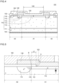
- Fig. 1 is a cross-sectional view illustrating the semiconductor device 100 according to the embodiment 1.
- " ⁇ " indicates recombination centers.
- Fig. 2 is an enlarged cross-sectional view of a main part of the semiconductor device 100 according to the embodiment 1. As illustrated in Fig.
- the semiconductor device 100 includes: a semiconductor base body 110; an insulation layer 120 that is formed on a surface of the semiconductor base body 110, has an opening 122 through which a surface of the semiconductor base body 110 is exposed; a surface electrode 130 that is connected to the semiconductor base body 110 at the opening 122; a back surface electrode 140 that is formed on a back surface side of the semiconductor base body 110; an equi-potential ring electrode (EQR electrode) 132 that is formed in the vicinity of an outermost periphery of a surface of the semiconductor base body 110; a protective insulation film 150 having an opening at a center portion thereof.
- EQR electrode equi-potential ring electrode
- the semiconductor device 100 according to the embodiment 1 is formed of an element forming region A1 and an outer peripheral region A2.
- a region on an inner peripheral side of an inner peripheral end B of a peripheral dopant region 114 described later is referred to as an element forming region A1
- a region disposed on an outer peripheral side of the inner peripheral end B of the peripheral dopant region 114 is referred to as an outer peripheral region A2.
- the recombination centers are formed in the semiconductor base body 110.
- the recombination centers may be formed by irradiating electron beams to the semiconductor base body 110 (performing annealing thereafter), or may be formed by applying heavy metal (for example, platinum or gold) to the semiconductor base body and, thereafter by diffusing heavy metal by heating.
- heavy metal for example, platinum or gold
- the dopant concentration of the drift region 112 falls within a range of from 1.0 ⁇ 10 13 cm -3 to 1.0 ⁇ 10 15 cm -3 .
- the channel stop region 116 is connected to the EQR electrode 132 positioned on the outer most periphery of the semiconductor base body 110.
- the dopant concentration in the channel stop region 116 is higher than the dopant concentration in the drift region 112.
- the p-type dopant region 113 includes a region that overlaps with the peripheral dopant region 114.
- a high concentration region 115 is formed in the region that overlaps with the peripheral dopant region 114.
- the high concentration region 115 is formed only in the region where the p-type dopant region 113 and the peripheral dopant region 114 overlap with each other.
- the high concentration region 115 may be formed on an inner peripheral side of the overlapping region besides the overlapping region.
- the dopant concentration of the high concentration region 115 is higher than the dopant concentration of other regions of the p-type dopant region 113, and is higher than the dopant concentration of the peripheral dopant region 114.
- the mode of carriers at the time of turning on or off switching in the semiconductor device 100 Before describing the mode of carriers at the time of turning on or off switching in the semiconductor device 100 according to the embodiment 1, the mode of carriers at the time of turning on or off switching in the conventional semiconductor device 900 is described.
- the holes that are carriers move in the semiconductor base body 910 from the surface electrode 930 toward the back surface electrode 940. Then, when a voltage is not applied between the surface electrode 930 and the back surface electrode 940 so that the switching is turned off, the holes in the semiconductor base body 910 move toward the surface electrode 930 and are recovered in the surface electrode 930.
- the present invention structure is a semiconductor device having substantially the same configuration as the semiconductor device 100 according to the embodiment 1.
- a peak of the recovery voltage after being raised is smaller than a waveform peak of the waveform of the "conventional structure", and an amplitude of ringing of the recovery voltage immediately behind the peak is small.
- the waveform of a recovery current of "the present invention structure” has a large reverse recovery current thus having a short reverse recovery time compared to the waveform of "the conventional structure”.
- the position of the inner peripheral end of the peripheral dopant region on the surface of the semiconductor base body differs from the corresponding position in the semiconductor device 100 according to the embodiment 1.
- the recombination centers are formed in the semiconductor base body 110, the inner peripheral end of the peripheral dopant region 114 is positioned on an outer peripheral side of an end portion of the opening 122, and the dopant concentration of the high concentration region 115 falls within a range of 1.0 ⁇ 10 16 cm -3 to 1.0 ⁇ 10 20 cm -3 .
- the holes or the like that are generated in the semiconductor base body 110 including the outer peripheral region A2 are recovered around the recombination centers and hence, a current amount per se that reaches the surface electrode 130 can be reduced. Accordingly, it is possible to reduce current density in the vicinity of a region where current density of a current that flows to the surface electrode 130 from an element forming region A1 via the p-type dopant region 113 and current density of a current that flows into the p-type dopant region 113 from the peripheral dopant region 114 and flows into the surface electrode 130 overlap with each other and hence, the increase of a temperature can be suppressed. As a result, a breakdown strength can be enhanced.
- the present invention has been described based on the embodiments described above.
- the present invention is not limited to the above-mentioned embodiments.
- the present invention can be carried out in various modes without departing from the gist of the present invention.
- the following modifications are also conceivable.
Landscapes
- Electrodes Of Semiconductors (AREA)
Applications Claiming Priority (1)
| Application Number | Priority Date | Filing Date | Title |
|---|---|---|---|
| JP2022210085A JP7821721B2 (ja) | 2022-12-27 | 2022-12-27 | 半導体装置 |
Publications (2)
| Publication Number | Publication Date |
|---|---|
| EP4394882A2 true EP4394882A2 (de) | 2024-07-03 |
| EP4394882A3 EP4394882A3 (de) | 2024-10-09 |
Family
ID=89473380
Family Applications (1)
| Application Number | Title | Priority Date | Filing Date |
|---|---|---|---|
| EP23212494.1A Pending EP4394882A3 (de) | 2022-12-27 | 2023-11-28 | Halbleiteranordnung |
Country Status (5)
| Country | Link |
|---|---|
| US (1) | US20240213308A1 (de) |
| EP (1) | EP4394882A3 (de) |
| JP (1) | JP7821721B2 (de) |
| CN (1) | CN118263334A (de) |
| TW (1) | TWI871110B (de) |
Citations (1)
| Publication number | Priority date | Publication date | Assignee | Title |
|---|---|---|---|---|
| JPH10335679A (ja) | 1997-06-02 | 1998-12-18 | Fuji Electric Co Ltd | ダイオードとその製造方法 |
Family Cites Families (16)
| Publication number | Priority date | Publication date | Assignee | Title |
|---|---|---|---|---|
| JP4843253B2 (ja) * | 2005-05-23 | 2011-12-21 | 株式会社東芝 | 電力用半導体装置 |
| JP2008147362A (ja) * | 2006-12-08 | 2008-06-26 | Toyota Central R&D Labs Inc | 半導体装置 |
| JP5716865B2 (ja) * | 2012-04-13 | 2015-05-13 | 三菱電機株式会社 | ダイオード |
| JP2014056976A (ja) * | 2012-09-13 | 2014-03-27 | Fuji Electric Co Ltd | 半導体装置およびその製造方法 |
| JP5971414B2 (ja) * | 2013-06-12 | 2016-08-17 | 三菱電機株式会社 | 半導体装置 |
| KR20150073607A (ko) * | 2013-12-23 | 2015-07-01 | 삼성전기주식회사 | 다이오드 소자 및 그의 제조 방법 |
| US11088031B2 (en) * | 2014-11-19 | 2021-08-10 | Key Foundry Co., Ltd. | Semiconductor and method of fabricating the same |
| JP6637012B2 (ja) * | 2016-11-10 | 2020-01-29 | ローム株式会社 | 半導体装置 |
| US10347714B2 (en) * | 2016-11-10 | 2019-07-09 | Rohm Co., Ltd. | Semiconductor device |
| JP6820738B2 (ja) * | 2016-12-27 | 2021-01-27 | 三菱電機株式会社 | 半導体装置、電力変換装置および半導体装置の製造方法 |
| JP2018157040A (ja) * | 2017-03-16 | 2018-10-04 | ローム株式会社 | 半導体装置 |
| US20200176600A1 (en) * | 2018-12-03 | 2020-06-04 | Vanguard International Semiconductor Corporation | High-voltage semiconductor devices and methods for manufacturing the same |
| JP7296907B2 (ja) * | 2020-03-10 | 2023-06-23 | 株式会社東芝 | 半導体装置 |
| JP7034214B2 (ja) * | 2020-06-29 | 2022-03-11 | ローム株式会社 | 半導体装置 |
| JP2022108157A (ja) * | 2021-01-12 | 2022-07-25 | キオクシア株式会社 | 半導体装置 |
| TWI818371B (zh) * | 2021-01-12 | 2023-10-11 | 立錡科技股份有限公司 | 高壓元件及其製造方法 |
-
2022
- 2022-12-27 JP JP2022210085A patent/JP7821721B2/ja active Active
-
2023
- 2023-11-28 TW TW112145964A patent/TWI871110B/zh active
- 2023-11-28 EP EP23212494.1A patent/EP4394882A3/de active Pending
- 2023-12-15 CN CN202311737416.7A patent/CN118263334A/zh active Pending
- 2023-12-25 US US18/395,627 patent/US20240213308A1/en active Pending
Patent Citations (1)
| Publication number | Priority date | Publication date | Assignee | Title |
|---|---|---|---|---|
| JPH10335679A (ja) | 1997-06-02 | 1998-12-18 | Fuji Electric Co Ltd | ダイオードとその製造方法 |
Also Published As
| Publication number | Publication date |
|---|---|
| US20240213308A1 (en) | 2024-06-27 |
| EP4394882A3 (de) | 2024-10-09 |
| TW202441786A (zh) | 2024-10-16 |
| TWI871110B (zh) | 2025-01-21 |
| JP2024093593A (ja) | 2024-07-09 |
| CN118263334A (zh) | 2024-06-28 |
| JP7821721B2 (ja) | 2026-02-27 |
Similar Documents
| Publication | Publication Date | Title |
|---|---|---|
| US11081598B2 (en) | Trench MOS Schottky diode | |
| JP6065154B2 (ja) | 炭化珪素半導体装置 | |
| US11569225B2 (en) | Semiconductor device | |
| EP2219224A1 (de) | Halbleiterbauelement | |
| JP6496992B2 (ja) | 半導体装置 | |
| US7915705B2 (en) | SiC semiconductor device having outer periphery structure | |
| CN105210187A (zh) | 半导体装置 | |
| US9793343B2 (en) | Semiconductor device | |
| US20130221477A1 (en) | Semiconductor device | |
| KR20120121344A (ko) | 반도체장치 | |
| JP7337739B2 (ja) | 半導体装置 | |
| US9666579B2 (en) | Semiconductor device | |
| EP3483940A1 (de) | Halbleiterbauelement und verfahren zur herstellung davon | |
| JP2024501237A (ja) | 絶縁トレンチゲート電極を有するパワー半導体デバイスおよびパワー半導体デバイスを製造する方法 | |
| JP7458257B2 (ja) | 半導体装置、インバータ回路、駆動装置、車両、及び、昇降機 | |
| EP3154091A1 (de) | Rückwärtsleitendes halbleiterbauelement | |
| US8476732B2 (en) | Semiconductor device | |
| JP2023043340A (ja) | 半導体装置 | |
| JP7321820B2 (ja) | 半導体装置、インバータ回路、駆動装置、車両、及び、昇降機 | |
| EP4394882A2 (de) | Halbleiteranordnung | |
| JP2016174031A (ja) | 半導体装置 | |
| US11621321B2 (en) | Semiconductor device | |
| JP7278913B2 (ja) | 半導体装置、半導体装置の製造方法、インバータ回路、駆動装置、車両、及び、昇降機 | |
| JP2010093080A (ja) | 半導体装置 | |
| JP2005175161A (ja) | 半導体装置及び製造方法 |
Legal Events
| Date | Code | Title | Description |
|---|---|---|---|
| PUAI | Public reference made under article 153(3) epc to a published international application that has entered the european phase |
Free format text: ORIGINAL CODE: 0009012 |
|
| STAA | Information on the status of an ep patent application or granted ep patent |
Free format text: STATUS: REQUEST FOR EXAMINATION WAS MADE |
|
| 17P | Request for examination filed |
Effective date: 20231128 |
|
| AK | Designated contracting states |
Kind code of ref document: A2 Designated state(s): AL AT BE BG CH CY CZ DE DK EE ES FI FR GB GR HR HU IE IS IT LI LT LU LV MC ME MK MT NL NO PL PT RO RS SE SI SK SM TR |
|
| PUAL | Search report despatched |
Free format text: ORIGINAL CODE: 0009013 |
|
| AK | Designated contracting states |
Kind code of ref document: A3 Designated state(s): AL AT BE BG CH CY CZ DE DK EE ES FI FR GB GR HR HU IE IS IT LI LT LU LV MC ME MK MT NL NO PL PT RO RS SE SI SK SM TR |
|
| RIC1 | Information provided on ipc code assigned before grant |
Ipc: H01L 29/861 20060101ALI20240904BHEP Ipc: H01L 29/32 20060101ALI20240904BHEP Ipc: H01L 29/06 20060101AFI20240904BHEP |