EP4289994A1 - Nitridhalbleitersubstrat und verfahren zur herstellung davon - Google Patents
Nitridhalbleitersubstrat und verfahren zur herstellung davon Download PDFInfo
- Publication number
- EP4289994A1 EP4289994A1 EP22749449.9A EP22749449A EP4289994A1 EP 4289994 A1 EP4289994 A1 EP 4289994A1 EP 22749449 A EP22749449 A EP 22749449A EP 4289994 A1 EP4289994 A1 EP 4289994A1
- Authority
- EP
- European Patent Office
- Prior art keywords
- nitride semiconductor
- layer
- substrate
- single crystal
- film
- Prior art date
- Legal status (The legal status is an assumption and is not a legal conclusion. Google has not performed a legal analysis and makes no representation as to the accuracy of the status listed.)
- Pending
Links
- 239000000758 substrate Substances 0.000 title claims abstract description 142
- 239000004065 semiconductor Substances 0.000 title claims abstract description 73
- 150000004767 nitrides Chemical class 0.000 title claims abstract description 68
- 238000004519 manufacturing process Methods 0.000 title claims abstract description 15
- 229910021421 monocrystalline silicon Inorganic materials 0.000 claims abstract description 65
- 239000002131 composite material Substances 0.000 claims abstract description 52
- 239000010409 thin film Substances 0.000 claims abstract description 25
- 239000010410 layer Substances 0.000 claims description 119
- 239000010408 film Substances 0.000 claims description 48
- 239000012790 adhesive layer Substances 0.000 claims description 39
- 238000000034 method Methods 0.000 claims description 29
- VYPSYNLAJGMNEJ-UHFFFAOYSA-N Silicium dioxide Chemical compound O=[Si]=O VYPSYNLAJGMNEJ-UHFFFAOYSA-N 0.000 claims description 24
- 229910052814 silicon oxide Inorganic materials 0.000 claims description 24
- 239000000919 ceramic Substances 0.000 claims description 20
- 229910002704 AlGaN Inorganic materials 0.000 claims description 11
- 230000004888 barrier function Effects 0.000 claims description 10
- BOTDANWDWHJENH-UHFFFAOYSA-N Tetraethyl orthosilicate Chemical compound CCO[Si](OCC)(OCC)OCC BOTDANWDWHJENH-UHFFFAOYSA-N 0.000 claims description 6
- 229910052581 Si3N4 Inorganic materials 0.000 claims description 4
- 229910021420 polycrystalline silicon Inorganic materials 0.000 claims description 4
- PMHQVHHXPFUNSP-UHFFFAOYSA-M copper(1+);methylsulfanylmethane;bromide Chemical compound Br[Cu].CSC PMHQVHHXPFUNSP-UHFFFAOYSA-M 0.000 claims description 3
- 229920005591 polysilicon Polymers 0.000 claims description 3
- HQVNEWCFYHHQES-UHFFFAOYSA-N silicon nitride Chemical compound N12[Si]34N5[Si]62N3[Si]51N64 HQVNEWCFYHHQES-UHFFFAOYSA-N 0.000 claims description 3
- 230000008569 process Effects 0.000 description 12
- 230000000694 effects Effects 0.000 description 6
- 230000015572 biosynthetic process Effects 0.000 description 5
- 238000002488 metal-organic chemical vapour deposition Methods 0.000 description 5
- XCZXGTMEAKBVPV-UHFFFAOYSA-N trimethylgallium Chemical compound C[Ga](C)C XCZXGTMEAKBVPV-UHFFFAOYSA-N 0.000 description 5
- 230000000052 comparative effect Effects 0.000 description 4
- 230000005496 eutectics Effects 0.000 description 4
- 238000004518 low pressure chemical vapour deposition Methods 0.000 description 4
- 239000000463 material Substances 0.000 description 4
- 230000003287 optical effect Effects 0.000 description 4
- 230000009467 reduction Effects 0.000 description 4
- 239000002344 surface layer Substances 0.000 description 4
- JMASRVWKEDWRBT-UHFFFAOYSA-N Gallium nitride Chemical compound [Ga]#N JMASRVWKEDWRBT-UHFFFAOYSA-N 0.000 description 2
- 230000008859 change Effects 0.000 description 2
- 238000001816 cooling Methods 0.000 description 2
- 238000005336 cracking Methods 0.000 description 2
- 230000007423 decrease Effects 0.000 description 2
- 230000007547 defect Effects 0.000 description 2
- 239000000428 dust Substances 0.000 description 2
- 238000005530 etching Methods 0.000 description 2
- JLTRXTDYQLMHGR-UHFFFAOYSA-N trimethylaluminium Chemical compound C[Al](C)C JLTRXTDYQLMHGR-UHFFFAOYSA-N 0.000 description 2
- ZOXJGFHDIHLPTG-UHFFFAOYSA-N Boron Chemical compound [B] ZOXJGFHDIHLPTG-UHFFFAOYSA-N 0.000 description 1
- OAICVXFJPJFONN-UHFFFAOYSA-N Phosphorus Chemical compound [P] OAICVXFJPJFONN-UHFFFAOYSA-N 0.000 description 1
- QVGXLLKOCUKJST-UHFFFAOYSA-N atomic oxygen Chemical compound [O] QVGXLLKOCUKJST-UHFFFAOYSA-N 0.000 description 1
- 229910052796 boron Inorganic materials 0.000 description 1
- 239000012159 carrier gas Substances 0.000 description 1
- 239000007795 chemical reaction product Substances 0.000 description 1
- 230000001276 controlling effect Effects 0.000 description 1
- 238000007796 conventional method Methods 0.000 description 1
- 239000013078 crystal Substances 0.000 description 1
- 238000009792 diffusion process Methods 0.000 description 1
- 229910052733 gallium Inorganic materials 0.000 description 1
- 239000007789 gas Substances 0.000 description 1
- 238000000227 grinding Methods 0.000 description 1
- 230000006872 improvement Effects 0.000 description 1
- 239000012535 impurity Substances 0.000 description 1
- 238000010030 laminating Methods 0.000 description 1
- 229910052751 metal Inorganic materials 0.000 description 1
- 239000002184 metal Substances 0.000 description 1
- SIWVEOZUMHYXCS-UHFFFAOYSA-N oxo(oxoyttriooxy)yttrium Chemical compound O=[Y]O[Y]=O SIWVEOZUMHYXCS-UHFFFAOYSA-N 0.000 description 1
- 229910052760 oxygen Inorganic materials 0.000 description 1
- 239000001301 oxygen Substances 0.000 description 1
- 229910052698 phosphorus Inorganic materials 0.000 description 1
- 239000011574 phosphorus Substances 0.000 description 1
- 238000005498 polishing Methods 0.000 description 1
- 230000001105 regulatory effect Effects 0.000 description 1
- 229910052594 sapphire Inorganic materials 0.000 description 1
- 239000010980 sapphire Substances 0.000 description 1
- 229910052710 silicon Inorganic materials 0.000 description 1
- 238000005245 sintering Methods 0.000 description 1
- 235000013619 trace mineral Nutrition 0.000 description 1
- 239000011573 trace mineral Substances 0.000 description 1
- 229910052727 yttrium Inorganic materials 0.000 description 1
- VWQVUPCCIRVNHF-UHFFFAOYSA-N yttrium atom Chemical compound [Y] VWQVUPCCIRVNHF-UHFFFAOYSA-N 0.000 description 1
Images


Classifications
-
- C—CHEMISTRY; METALLURGY
- C30—CRYSTAL GROWTH
- C30B—SINGLE-CRYSTAL GROWTH; UNIDIRECTIONAL SOLIDIFICATION OF EUTECTIC MATERIAL OR UNIDIRECTIONAL DEMIXING OF EUTECTOID MATERIAL; REFINING BY ZONE-MELTING OF MATERIAL; PRODUCTION OF A HOMOGENEOUS POLYCRYSTALLINE MATERIAL WITH DEFINED STRUCTURE; SINGLE CRYSTALS OR HOMOGENEOUS POLYCRYSTALLINE MATERIAL WITH DEFINED STRUCTURE; AFTER-TREATMENT OF SINGLE CRYSTALS OR A HOMOGENEOUS POLYCRYSTALLINE MATERIAL WITH DEFINED STRUCTURE; APPARATUS THEREFOR
- C30B29/00—Single crystals or homogeneous polycrystalline material with defined structure characterised by the material or by their shape
- C30B29/02—Elements
- C30B29/06—Silicon
-
- H—ELECTRICITY
- H01—ELECTRIC ELEMENTS
- H01L—SEMICONDUCTOR DEVICES NOT COVERED BY CLASS H10
- H01L21/00—Processes or apparatus adapted for the manufacture or treatment of semiconductor or solid state devices or of parts thereof
- H01L21/02—Manufacture or treatment of semiconductor devices or of parts thereof
- H01L21/02104—Forming layers
- H01L21/02365—Forming inorganic semiconducting materials on a substrate
- H01L21/02367—Substrates
- H01L21/02428—Structure
-
- C—CHEMISTRY; METALLURGY
- C23—COATING METALLIC MATERIAL; COATING MATERIAL WITH METALLIC MATERIAL; CHEMICAL SURFACE TREATMENT; DIFFUSION TREATMENT OF METALLIC MATERIAL; COATING BY VACUUM EVAPORATION, BY SPUTTERING, BY ION IMPLANTATION OR BY CHEMICAL VAPOUR DEPOSITION, IN GENERAL; INHIBITING CORROSION OF METALLIC MATERIAL OR INCRUSTATION IN GENERAL
- C23C—COATING METALLIC MATERIAL; COATING MATERIAL WITH METALLIC MATERIAL; SURFACE TREATMENT OF METALLIC MATERIAL BY DIFFUSION INTO THE SURFACE, BY CHEMICAL CONVERSION OR SUBSTITUTION; COATING BY VACUUM EVAPORATION, BY SPUTTERING, BY ION IMPLANTATION OR BY CHEMICAL VAPOUR DEPOSITION, IN GENERAL
- C23C16/00—Chemical coating by decomposition of gaseous compounds, without leaving reaction products of surface material in the coating, i.e. chemical vapour deposition [CVD] processes
- C23C16/22—Chemical coating by decomposition of gaseous compounds, without leaving reaction products of surface material in the coating, i.e. chemical vapour deposition [CVD] processes characterised by the deposition of inorganic material, other than metallic material
- C23C16/30—Deposition of compounds, mixtures or solid solutions, e.g. borides, carbides, nitrides
- C23C16/34—Nitrides
-
- C—CHEMISTRY; METALLURGY
- C30—CRYSTAL GROWTH
- C30B—SINGLE-CRYSTAL GROWTH; UNIDIRECTIONAL SOLIDIFICATION OF EUTECTIC MATERIAL OR UNIDIRECTIONAL DEMIXING OF EUTECTOID MATERIAL; REFINING BY ZONE-MELTING OF MATERIAL; PRODUCTION OF A HOMOGENEOUS POLYCRYSTALLINE MATERIAL WITH DEFINED STRUCTURE; SINGLE CRYSTALS OR HOMOGENEOUS POLYCRYSTALLINE MATERIAL WITH DEFINED STRUCTURE; AFTER-TREATMENT OF SINGLE CRYSTALS OR A HOMOGENEOUS POLYCRYSTALLINE MATERIAL WITH DEFINED STRUCTURE; APPARATUS THEREFOR
- C30B25/00—Single-crystal growth by chemical reaction of reactive gases, e.g. chemical vapour-deposition growth
- C30B25/02—Epitaxial-layer growth
- C30B25/18—Epitaxial-layer growth characterised by the substrate
- C30B25/186—Epitaxial-layer growth characterised by the substrate being specially pre-treated by, e.g. chemical or physical means
-
- C—CHEMISTRY; METALLURGY
- C30—CRYSTAL GROWTH
- C30B—SINGLE-CRYSTAL GROWTH; UNIDIRECTIONAL SOLIDIFICATION OF EUTECTIC MATERIAL OR UNIDIRECTIONAL DEMIXING OF EUTECTOID MATERIAL; REFINING BY ZONE-MELTING OF MATERIAL; PRODUCTION OF A HOMOGENEOUS POLYCRYSTALLINE MATERIAL WITH DEFINED STRUCTURE; SINGLE CRYSTALS OR HOMOGENEOUS POLYCRYSTALLINE MATERIAL WITH DEFINED STRUCTURE; AFTER-TREATMENT OF SINGLE CRYSTALS OR A HOMOGENEOUS POLYCRYSTALLINE MATERIAL WITH DEFINED STRUCTURE; APPARATUS THEREFOR
- C30B29/00—Single crystals or homogeneous polycrystalline material with defined structure characterised by the material or by their shape
- C30B29/10—Inorganic compounds or compositions
- C30B29/38—Nitrides
-
- C—CHEMISTRY; METALLURGY
- C30—CRYSTAL GROWTH
- C30B—SINGLE-CRYSTAL GROWTH; UNIDIRECTIONAL SOLIDIFICATION OF EUTECTIC MATERIAL OR UNIDIRECTIONAL DEMIXING OF EUTECTOID MATERIAL; REFINING BY ZONE-MELTING OF MATERIAL; PRODUCTION OF A HOMOGENEOUS POLYCRYSTALLINE MATERIAL WITH DEFINED STRUCTURE; SINGLE CRYSTALS OR HOMOGENEOUS POLYCRYSTALLINE MATERIAL WITH DEFINED STRUCTURE; AFTER-TREATMENT OF SINGLE CRYSTALS OR A HOMOGENEOUS POLYCRYSTALLINE MATERIAL WITH DEFINED STRUCTURE; APPARATUS THEREFOR
- C30B29/00—Single crystals or homogeneous polycrystalline material with defined structure characterised by the material or by their shape
- C30B29/10—Inorganic compounds or compositions
- C30B29/40—AIIIBV compounds wherein A is B, Al, Ga, In or Tl and B is N, P, As, Sb or Bi
- C30B29/403—AIII-nitrides
- C30B29/406—Gallium nitride
-
- H—ELECTRICITY
- H01—ELECTRIC ELEMENTS
- H01L—SEMICONDUCTOR DEVICES NOT COVERED BY CLASS H10
- H01L21/00—Processes or apparatus adapted for the manufacture or treatment of semiconductor or solid state devices or of parts thereof
- H01L21/02—Manufacture or treatment of semiconductor devices or of parts thereof
- H01L21/02104—Forming layers
- H01L21/02365—Forming inorganic semiconducting materials on a substrate
- H01L21/02367—Substrates
- H01L21/0237—Materials
- H01L21/02373—Group 14 semiconducting materials
- H01L21/02381—Silicon, silicon germanium, germanium
-
- H—ELECTRICITY
- H01—ELECTRIC ELEMENTS
- H01L—SEMICONDUCTOR DEVICES NOT COVERED BY CLASS H10
- H01L21/00—Processes or apparatus adapted for the manufacture or treatment of semiconductor or solid state devices or of parts thereof
- H01L21/02—Manufacture or treatment of semiconductor devices or of parts thereof
- H01L21/02104—Forming layers
- H01L21/02365—Forming inorganic semiconducting materials on a substrate
- H01L21/02367—Substrates
- H01L21/0237—Materials
- H01L21/02387—Group 13/15 materials
- H01L21/02389—Nitrides
-
- H—ELECTRICITY
- H01—ELECTRIC ELEMENTS
- H01L—SEMICONDUCTOR DEVICES NOT COVERED BY CLASS H10
- H01L21/00—Processes or apparatus adapted for the manufacture or treatment of semiconductor or solid state devices or of parts thereof
- H01L21/02—Manufacture or treatment of semiconductor devices or of parts thereof
- H01L21/02104—Forming layers
- H01L21/02365—Forming inorganic semiconducting materials on a substrate
- H01L21/02436—Intermediate layers between substrates and deposited layers
- H01L21/02439—Materials
- H01L21/02441—Group 14 semiconducting materials
- H01L21/0245—Silicon, silicon germanium, germanium
-
- H—ELECTRICITY
- H01—ELECTRIC ELEMENTS
- H01L—SEMICONDUCTOR DEVICES NOT COVERED BY CLASS H10
- H01L21/00—Processes or apparatus adapted for the manufacture or treatment of semiconductor or solid state devices or of parts thereof
- H01L21/02—Manufacture or treatment of semiconductor devices or of parts thereof
- H01L21/02104—Forming layers
- H01L21/02365—Forming inorganic semiconducting materials on a substrate
- H01L21/02436—Intermediate layers between substrates and deposited layers
- H01L21/02439—Materials
- H01L21/02488—Insulating materials
-
- H—ELECTRICITY
- H01—ELECTRIC ELEMENTS
- H01L—SEMICONDUCTOR DEVICES NOT COVERED BY CLASS H10
- H01L21/00—Processes or apparatus adapted for the manufacture or treatment of semiconductor or solid state devices or of parts thereof
- H01L21/02—Manufacture or treatment of semiconductor devices or of parts thereof
- H01L21/02104—Forming layers
- H01L21/02365—Forming inorganic semiconducting materials on a substrate
- H01L21/02436—Intermediate layers between substrates and deposited layers
- H01L21/02494—Structure
- H01L21/02496—Layer structure
- H01L21/02505—Layer structure consisting of more than two layers
-
- H—ELECTRICITY
- H01—ELECTRIC ELEMENTS
- H01L—SEMICONDUCTOR DEVICES NOT COVERED BY CLASS H10
- H01L21/00—Processes or apparatus adapted for the manufacture or treatment of semiconductor or solid state devices or of parts thereof
- H01L21/02—Manufacture or treatment of semiconductor devices or of parts thereof
- H01L21/02104—Forming layers
- H01L21/02365—Forming inorganic semiconducting materials on a substrate
- H01L21/02518—Deposited layers
- H01L21/02521—Materials
- H01L21/02538—Group 13/15 materials
- H01L21/0254—Nitrides
-
- H—ELECTRICITY
- H01—ELECTRIC ELEMENTS
- H01L—SEMICONDUCTOR DEVICES NOT COVERED BY CLASS H10
- H01L21/00—Processes or apparatus adapted for the manufacture or treatment of semiconductor or solid state devices or of parts thereof
- H01L21/02—Manufacture or treatment of semiconductor devices or of parts thereof
- H01L21/02104—Forming layers
- H01L21/02365—Forming inorganic semiconducting materials on a substrate
- H01L21/02612—Formation types
- H01L21/02617—Deposition types
- H01L21/0262—Reduction or decomposition of gaseous compounds, e.g. CVD
-
- H—ELECTRICITY
- H01—ELECTRIC ELEMENTS
- H01L—SEMICONDUCTOR DEVICES NOT COVERED BY CLASS H10
- H01L21/00—Processes or apparatus adapted for the manufacture or treatment of semiconductor or solid state devices or of parts thereof
- H01L21/02—Manufacture or treatment of semiconductor devices or of parts thereof
- H01L21/02104—Forming layers
- H01L21/02365—Forming inorganic semiconducting materials on a substrate
- H01L21/02436—Intermediate layers between substrates and deposited layers
- H01L21/02439—Materials
- H01L21/02491—Conductive materials
-
- H—ELECTRICITY
- H01—ELECTRIC ELEMENTS
- H01L—SEMICONDUCTOR DEVICES NOT COVERED BY CLASS H10
- H01L21/00—Processes or apparatus adapted for the manufacture or treatment of semiconductor or solid state devices or of parts thereof
- H01L21/02—Manufacture or treatment of semiconductor devices or of parts thereof
- H01L21/02104—Forming layers
- H01L21/02365—Forming inorganic semiconducting materials on a substrate
- H01L21/02518—Deposited layers
- H01L21/02521—Materials
- H01L21/02524—Group 14 semiconducting materials
- H01L21/02532—Silicon, silicon germanium, germanium
Definitions
- a MOCVD method which is one of methods for manufacturing a semiconductor thin film is commonly used because the method has excellent large-diameter formability and mass productivity and can form a uniform thin film crystal.
- Nitride semiconductors represented by GaN are promising as a next-generation semiconductor material beyond the limit of a Si material.
- GaN, SiC, sapphire, Si, etc. are used for a substrate for epitaxially growing GaN in the MOCVD method.
- Si is most inexpensive and a substrate useful for large-diameter formability.
- GaN and Si have difference in a thermal expansion coefficient, tensile stress is applied to GaN in a cooling step after the epitaxial film-formation.
- problems such as difficulty in forming a thick epitaxial layer, occurrence of cracking, and necessity of a complex stress-relaxing layer.
- This composite substrate for growing GaN is constituted with: a composite substrate having a polycrystalline ceramic core, a first adhesive layer bonded to an entirety of the polycrystalline ceramic core, a conductive layer bonded to an entirety of the first adhesive layer as necessary, a second adhesive layer bonded to an entirety of the conductive layer or to the entirety of the first adhesive layer, and a barrier layer bonded to an entirety of the second adhesive layer; a silicon oxide layer bonded to only one surface of the composite substrate; and a single crystal silicon layer bonded to the silicon oxide layer.
- this composite substrate for growing GaN enables to produce a GaN epitaxial growth substrate that has a large diameter and a thick epitaxial layer and that causes no cracking.
- the substrate since the difference from GaN in the thermal expansion coefficient is small, the substrate is hardly warped in growing GaN or cooling, and a warp of the substrate after the film formation can be regulated to be small.
- the substrate since a large part of the composite substrate for growing GaN is made of ceramics, the substrate itself is extremely hard and hardly plastically deformed, and wafer breakage, which has not been solved with GaN/Si, does not occur.
- reaction mark a eutectic reaction product between Si and Ga due to melt-back etching is likely to be generated.
- This reaction mark not only decreases a device yield but also probably becomes a dust source in a device process, which may contaminate a process line. Thus, it is extremely important to control generation of the reaction mark.
- Patent Document 1 discloses art for removing the reaction mark after the epitaxial growth of GaN, but does not disclose a method for controlling the reaction mark by making contrivance in the epitaxial growth.
- Patent Documents 2 and 3 disclose art about forming a III-V group semiconductor thin film on the composite substrate for growing GaN, but do not describe a reduction in defects in the film formation. There has been no literature disclosing art about a reduction in defects in forming a semiconductor thin film on the composite substrate for growing GaN.
- the single crystal silicon in a surface layer of the composite substrate for growing GaN and Ga in trimethylgallium (TMGa) used as a Ga source may be reacted to generate the reaction mark.
- TMGa trimethylgallium
- GaN growth on the composite substrate for growing GaN tends to generate the reaction mark. This is because an edge of the surface layer of the single crystal silicon layer on the composite substrate for growing GaN, which has a complex shape ( FIG.
- An object of the present invention is to provide: a nitride semiconductor substrate with inhibited generation of the reaction mark; and a manufacturing method therefor.
- the present invention provides a nitride semiconductor substrate comprising a Ga-containing nitride semiconductor thin film formed on a substrate for film-forming in which a single crystal silicon layer is formed on a composite substrate in which a plurality of layers is bonded, wherein the nitride semiconductor substrate has a region where the Ga-containing nitride semiconductor thin film is not formed inward from an edge of the single crystal silicon layer being a growth surface of the nitride semiconductor thin film.
- Such a nitride semiconductor substrate can inhibit the generation of the reaction mark due to the eutectic reaction between the single crystal silicon and Ga.
- the region where the film is not formed is preferably a region with 0.3 mm or longer and shorter than 3 mm inward from the edge of the single crystal silicon layer.
- Such a nitride semiconductor substrate can more improve the effect of the present invention.
- the single crystal silicon layer preferably has a thickness of 300 to 500 nm.
- Such a nitride semiconductor substrate can further improve the effect of the present invention.
- Such a nitride semiconductor substrate is useful as a nitride semiconductor substrate required in recent years, and can still further improve the effect of the present invention.
- the nitride semiconductor substrate using such a substrate for film-forming can regulate a warp of the substrate after the film formation to be small.
- the polycrystalline ceramic core preferably contains aluminum nitride.
- the first adhesive layer and the second adhesive layer preferably contain tetraethyl orthosilicate (TEOS) or silicon oxide (SiO 2 ), the conductive layer preferably has a polysilicon layer, and the barrier layer preferably contains silicon nitride.
- TEOS tetraethyl orthosilicate
- SiO 2 silicon oxide
- the conductive layer preferably has a polysilicon layer
- the barrier layer preferably contains silicon nitride.
- Such a nitride semiconductor substrate can regulate the warp of the substrate after the film formation to be further smaller, and can form a thick nitride semiconductor thin film.
- the present invention also provides a method for manufacturing a nitride semiconductor substrate, the method comprising steps of:
- the composite substrate in which the plurality of the layers is bonded is preferably a composite substrate having: a polycrystalline ceramic core; a first adhesive layer bonded to an entirety of the polycrystalline ceramic core; a conductive layer bonded to an entirety of the first adhesive layer as necessary; a second adhesive layer bonded to an entirety of the conductive layer or to the entirety of the first adhesive layer; and a barrier layer bonded to an entirety of the second adhesive layer.
- Such a method for manufacturing a nitride semiconductor substrate can more improve the effect of the present invention.
- the inventive nitride semiconductor substrate can inhibit the generation of the reaction mark due to the eutectic reaction between the single crystal silicon and Ga. Therefore, a high-quality nitride semiconductor substrate can be obtained, and in manufacturing a device using this substrate, improvement of a device yield and higher precision can be attempted.
- the present invention is a method for manufacturing a nitride semiconductor substrate, the method comprising steps of:
- the composite substrate for growing GaN can be constituted with: the composite substrate having a polycrystalline ceramic core 1, a first adhesive layer 2 bonded to an entirety of the polycrystalline ceramic core, a conductive layer 3 bonded to an entirety of the first adhesive layer, a second adhesive layer 4 bonded to an entirety of the conductive layer, and a barrier layer 5 bonded to an entirety of the second adhesive layer; a silicon oxide layer 6 bonded only on one surface of the composite substrate; and a single crystal silicon layer 7 bonded to the silicon oxide layer, as illustrated in FIG. 3 for example.
- the polycrystalline ceramic core 1 can contain aluminum nitride, and sintered with a sintering auxiliary at a high temperature of, for example, 1800°C to preferably have a thickness of approximately 600 to 1150 um.
- the polycrystalline ceramic core 1 is formed with a thickness of the SEMI standard of the single crystal silicon substrate in many cases.
- the first adhesive layer 2 and the second adhesive layer 4 can be layers containing tetraethyl orthosilicate (TEOS) or silicon oxide (SiO 2 ), and deposited by, for example, an LPCVD process, a CVD process, etc. to preferably have a thickness of 100 nm.
- TEOS tetraethyl orthosilicate
- SiO 2 silicon oxide
- the composite substrate for growing GaN can be placed in, for example, a wafer pocket called as a satellite, as FIG. 2 .
- a wafer pocket called as a satellite, as FIG. 2 .
- TMGa trimethylaluminum
- NH 3 a N source
- the carrier gas can be N 2 and H 2 , or any one thereof, and the process temperature is preferably, for example, approximately 900 to 1200°C.
- a composite substrate for growing GaN with 150 mm in diameter constituted with: a composite substrate having a polycrystalline ceramic core, a first adhesive layer (SiO 2 ) bonded to an entirety of the polycrystalline ceramic core, a conductive layer (poly-Si) bonded to an entirety of the first adhesive layer, a second adhesive layer (SiO 2 ) bonded to an entirety of the conductive layer, and a barrier layer (Si 3 N 4 ) bonded to an entirety of the second adhesive layer; a silicon oxide layer bonded to only one surface of the composite substrate; and a single crystal silicon layer bonded to the silicon oxide layer.
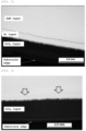
- a ring-shaped member composed of SiC was placed on the composite substrate for growing GaN so that the single crystal silicon layer of the composite substrate for growing GaN covered a region with 0.3 mm inward from the edge.
- Example 6 An epitaxial growth was performed under the same condition as in Example except that the ring-shaped member was not placed. The generation state of a reaction mark on the periphery was checked in the same manner as in Example. FIG. 6 shows the result. As shown in FIG. 6 , the generation of the reaction mark can be observed.
- the inventive nitride semiconductor substrate can be a nitride semiconductor substrate with inhibited generation of the reaction mark.
Landscapes
- Engineering & Computer Science (AREA)
- Chemical & Material Sciences (AREA)
- Materials Engineering (AREA)
- Condensed Matter Physics & Semiconductors (AREA)
- General Physics & Mathematics (AREA)
- Manufacturing & Machinery (AREA)
- Computer Hardware Design (AREA)
- Microelectronics & Electronic Packaging (AREA)
- Power Engineering (AREA)
- Physics & Mathematics (AREA)
- Organic Chemistry (AREA)
- Metallurgy (AREA)
- Crystallography & Structural Chemistry (AREA)
- Chemical Kinetics & Catalysis (AREA)
- General Chemical & Material Sciences (AREA)
- Inorganic Chemistry (AREA)
- Mechanical Engineering (AREA)
- Recrystallisation Techniques (AREA)
- Crystals, And After-Treatments Of Crystals (AREA)
- Chemical Vapour Deposition (AREA)
Applications Claiming Priority (2)
| Application Number | Priority Date | Filing Date | Title |
|---|---|---|---|
| JP2021017688 | 2021-02-05 | ||
| PCT/JP2022/001273 WO2022168572A1 (ja) | 2021-02-05 | 2022-01-17 | 窒化物半導体基板及びその製造方法 |
Publications (1)
| Publication Number | Publication Date |
|---|---|
| EP4289994A1 true EP4289994A1 (de) | 2023-12-13 |
Family
ID=82740621
Family Applications (1)
| Application Number | Title | Priority Date | Filing Date |
|---|---|---|---|
| EP22749449.9A Pending EP4289994A1 (de) | 2021-02-05 | 2022-01-17 | Nitridhalbleitersubstrat und verfahren zur herstellung davon |
Country Status (6)
| Country | Link |
|---|---|
| EP (1) | EP4289994A1 (de) |
| JP (1) | JP7290182B2 (de) |
| KR (1) | KR20230137921A (de) |
| CN (1) | CN116848296A (de) |
| TW (1) | TW202246597A (de) |
| WO (1) | WO2022168572A1 (de) |
Family Cites Families (8)
| Publication number | Priority date | Publication date | Assignee | Title |
|---|---|---|---|---|
| JP2006216815A (ja) * | 2005-02-04 | 2006-08-17 | Yamaha Corp | フィールド酸化膜形成法 |
| JP5244364B2 (ja) * | 2007-10-16 | 2013-07-24 | 株式会社半導体エネルギー研究所 | 半導体装置及びその作製方法 |
| JP6261388B2 (ja) | 2014-03-05 | 2018-01-17 | 信越半導体株式会社 | 半導体エピタキシャルウェーハの製造方法 |
| CN109844184B (zh) | 2016-06-14 | 2021-11-30 | 克罗米斯有限公司 | 用于功率应用和射频应用的工程化衬底结构 |
| US10355120B2 (en) | 2017-01-18 | 2019-07-16 | QROMIS, Inc. | Gallium nitride epitaxial structures for power devices |
| US10734303B2 (en) * | 2017-11-06 | 2020-08-04 | QROMIS, Inc. | Power and RF devices implemented using an engineered substrate structure |
| GB2574879B (en) * | 2018-06-22 | 2022-12-28 | X Fab Semiconductor Foundries Gmbh | Substrates for III-nitride epitaxy |
| JP2021195299A (ja) * | 2020-06-09 | 2021-12-27 | 信越化学工業株式会社 | Iii族窒化物系エピタキシャル成長用基板とその製造方法 |
-
2022
- 2022-01-17 CN CN202280012925.0A patent/CN116848296A/zh active Pending
- 2022-01-17 KR KR1020237026247A patent/KR20230137921A/ko unknown
- 2022-01-17 EP EP22749449.9A patent/EP4289994A1/de active Pending
- 2022-01-17 WO PCT/JP2022/001273 patent/WO2022168572A1/ja active Application Filing
- 2022-01-24 TW TW111102798A patent/TW202246597A/zh unknown
- 2022-02-01 JP JP2022014170A patent/JP7290182B2/ja active Active
Also Published As
| Publication number | Publication date |
|---|---|
| CN116848296A (zh) | 2023-10-03 |
| TW202246597A (zh) | 2022-12-01 |
| WO2022168572A1 (ja) | 2022-08-11 |
| JP7290182B2 (ja) | 2023-06-13 |
| KR20230137921A (ko) | 2023-10-05 |
| JP2022120821A (ja) | 2022-08-18 |
Similar Documents
| Publication | Publication Date | Title |
|---|---|---|
| JP5371430B2 (ja) | 半導体基板並びにハイドライド気相成長法により自立半導体基板を製造するための方法及びそれに使用されるマスク層 | |
| US6176925B1 (en) | Detached and inverted epitaxial regrowth & methods | |
| TWI531081B (zh) | 半導體裝置的製造方法 | |
| EP2519982B1 (de) | Epitaxialwafer, verfahren zu dessen herstellung und verfahren zur herstellung eines led-chips | |
| CN107978659B (zh) | 制造氮化镓衬底的方法 | |
| EP4289994A1 (de) | Nitridhalbleitersubstrat und verfahren zur herstellung davon | |
| US8853064B2 (en) | Method of manufacturing substrate | |
| US7112243B2 (en) | Method for producing Group III nitride compound semiconductor | |
| US9947530B2 (en) | Method of manufacturing nitride semiconductor substrate | |
| EP4289995A1 (de) | Nitridhalbleitersubstrat und verfahren zur herstellung davon | |
| WO2023017712A1 (ja) | 窒化物半導体基板及びその製造方法 | |
| JP7207588B1 (ja) | Iii族窒化物半導体ウエーハ及びその製造方法 | |
| KR101474373B1 (ko) | 반도체 기판 및 그 제조 방법 | |
| KR101480949B1 (ko) | 화합물 반도체 기판 및 이의 제조 방법 | |
| WO2020066544A1 (ja) | エピタキシャルウェーハの製造方法、エピタキシャル成長用シリコン系基板及びエピタキシャルウェーハ | |
| JP5631952B2 (ja) | 基板の製造方法 | |
| CN115386959A (zh) | 一种氮化镓生长方法及氮化镓 | |
| KR20150020498A (ko) | 반도체 기판 및 그 제조 방법 |
Legal Events
| Date | Code | Title | Description |
|---|---|---|---|
| STAA | Information on the status of an ep patent application or granted ep patent |
Free format text: STATUS: THE INTERNATIONAL PUBLICATION HAS BEEN MADE |
|
| PUAI | Public reference made under article 153(3) epc to a published international application that has entered the european phase |
Free format text: ORIGINAL CODE: 0009012 |
|
| STAA | Information on the status of an ep patent application or granted ep patent |
Free format text: STATUS: REQUEST FOR EXAMINATION WAS MADE |
|
| 17P | Request for examination filed |
Effective date: 20230717 |
|
| AK | Designated contracting states |
Kind code of ref document: A1 Designated state(s): AL AT BE BG CH CY CZ DE DK EE ES FI FR GB GR HR HU IE IS IT LI LT LU LV MC MK MT NL NO PL PT RO RS SE SI SK SM TR |
|
| DAV | Request for validation of the european patent (deleted) | ||
| DAX | Request for extension of the european patent (deleted) |