EP4258337A1 - Insulated board and power converter - Google Patents
Insulated board and power converter Download PDFInfo
- Publication number
- EP4258337A1 EP4258337A1 EP21900266.4A EP21900266A EP4258337A1 EP 4258337 A1 EP4258337 A1 EP 4258337A1 EP 21900266 A EP21900266 A EP 21900266A EP 4258337 A1 EP4258337 A1 EP 4258337A1
- Authority
- EP
- European Patent Office
- Prior art keywords
- conductor
- conductors
- insulating plate
- insulating
- insulating substrate
- Prior art date
- Legal status (The legal status is an assumption and is not a legal conclusion. Google has not performed a legal analysis and makes no representation as to the accuracy of the status listed.)
- Pending
Links
- 239000004020 conductor Substances 0.000 claims abstract description 290
- 239000000758 substrate Substances 0.000 claims abstract description 123
- 230000017525 heat dissipation Effects 0.000 claims abstract description 68
- 238000006243 chemical reaction Methods 0.000 claims abstract description 59
- 239000004065 semiconductor Substances 0.000 claims description 64
- 150000001875 compounds Chemical class 0.000 claims description 8
- 230000003071 parasitic effect Effects 0.000 abstract description 17
- 230000000694 effects Effects 0.000 description 9
- 230000001681 protective effect Effects 0.000 description 9
- 239000010949 copper Substances 0.000 description 8
- 239000010410 layer Substances 0.000 description 8
- HBMJWWWQQXIZIP-UHFFFAOYSA-N silicon carbide Chemical compound [Si+]#[C-] HBMJWWWQQXIZIP-UHFFFAOYSA-N 0.000 description 6
- 238000012986 modification Methods 0.000 description 5
- 230000004048 modification Effects 0.000 description 5
- 229910010271 silicon carbide Inorganic materials 0.000 description 5
- RYGMFSIKBFXOCR-UHFFFAOYSA-N Copper Chemical compound [Cu] RYGMFSIKBFXOCR-UHFFFAOYSA-N 0.000 description 4
- JMASRVWKEDWRBT-UHFFFAOYSA-N Gallium nitride Chemical compound [Ga]#N JMASRVWKEDWRBT-UHFFFAOYSA-N 0.000 description 4
- 239000003990 capacitor Substances 0.000 description 4
- 229910052802 copper Inorganic materials 0.000 description 4
- 239000000463 material Substances 0.000 description 4
- 229910002601 GaN Inorganic materials 0.000 description 3
- 229910052782 aluminium Inorganic materials 0.000 description 3
- XAGFODPZIPBFFR-UHFFFAOYSA-N aluminium Chemical compound [Al] XAGFODPZIPBFFR-UHFFFAOYSA-N 0.000 description 3
- 239000000919 ceramic Substances 0.000 description 3
- 239000007769 metal material Substances 0.000 description 3
- 239000002356 single layer Substances 0.000 description 3
- 239000002131 composite material Substances 0.000 description 2
- 238000001816 cooling Methods 0.000 description 2
- 239000010931 gold Substances 0.000 description 2
- 238000000034 method Methods 0.000 description 2
- 239000002245 particle Substances 0.000 description 2
- 239000011347 resin Substances 0.000 description 2
- 229920005989 resin Polymers 0.000 description 2
- 229910000838 Al alloy Inorganic materials 0.000 description 1
- 229910000962 AlSiC Inorganic materials 0.000 description 1
- XEEYBQQBJWHFJM-UHFFFAOYSA-N Iron Chemical compound [Fe] XEEYBQQBJWHFJM-UHFFFAOYSA-N 0.000 description 1
- FYYHWMGAXLPEAU-UHFFFAOYSA-N Magnesium Chemical compound [Mg] FYYHWMGAXLPEAU-UHFFFAOYSA-N 0.000 description 1
- 230000015572 biosynthetic process Effects 0.000 description 1
- 230000006866 deterioration Effects 0.000 description 1
- AJNVQOSZGJRYEI-UHFFFAOYSA-N digallium;oxygen(2-) Chemical compound [O-2].[O-2].[O-2].[Ga+3].[Ga+3] AJNVQOSZGJRYEI-UHFFFAOYSA-N 0.000 description 1
- 238000007599 discharging Methods 0.000 description 1
- PCHJSUWPFVWCPO-UHFFFAOYSA-N gold Chemical compound [Au] PCHJSUWPFVWCPO-UHFFFAOYSA-N 0.000 description 1
- 229910052737 gold Inorganic materials 0.000 description 1
- 239000011810 insulating material Substances 0.000 description 1
- 229910052749 magnesium Inorganic materials 0.000 description 1
- 239000011777 magnesium Substances 0.000 description 1
- 238000000465 moulding Methods 0.000 description 1
- 238000004088 simulation Methods 0.000 description 1
- 229910000679 solder Inorganic materials 0.000 description 1
Images


Classifications
-
- H—ELECTRICITY
- H01—ELECTRIC ELEMENTS
- H01L—SEMICONDUCTOR DEVICES NOT COVERED BY CLASS H10
- H01L23/00—Details of semiconductor or other solid state devices
- H01L23/34—Arrangements for cooling, heating, ventilating or temperature compensation ; Temperature sensing arrangements
- H01L23/36—Selection of materials, or shaping, to facilitate cooling or heating, e.g. heatsinks
- H01L23/373—Cooling facilitated by selection of materials for the device or materials for thermal expansion adaptation, e.g. carbon
- H01L23/3735—Laminates or multilayers, e.g. direct bond copper ceramic substrates
-
- H—ELECTRICITY
- H01—ELECTRIC ELEMENTS
- H01L—SEMICONDUCTOR DEVICES NOT COVERED BY CLASS H10
- H01L23/00—Details of semiconductor or other solid state devices
- H01L23/34—Arrangements for cooling, heating, ventilating or temperature compensation ; Temperature sensing arrangements
- H01L23/36—Selection of materials, or shaping, to facilitate cooling or heating, e.g. heatsinks
- H01L23/367—Cooling facilitated by shape of device
- H01L23/3677—Wire-like or pin-like cooling fins or heat sinks
-
- H—ELECTRICITY
- H01—ELECTRIC ELEMENTS
- H01L—SEMICONDUCTOR DEVICES NOT COVERED BY CLASS H10
- H01L25/00—Assemblies consisting of a plurality of individual semiconductor or other solid state devices ; Multistep manufacturing processes thereof
- H01L25/03—Assemblies consisting of a plurality of individual semiconductor or other solid state devices ; Multistep manufacturing processes thereof all the devices being of a type provided for in the same subgroup of groups H01L27/00 - H01L33/00, or in a single subclass of H10K, H10N, e.g. assemblies of rectifier diodes
- H01L25/04—Assemblies consisting of a plurality of individual semiconductor or other solid state devices ; Multistep manufacturing processes thereof all the devices being of a type provided for in the same subgroup of groups H01L27/00 - H01L33/00, or in a single subclass of H10K, H10N, e.g. assemblies of rectifier diodes the devices not having separate containers
- H01L25/07—Assemblies consisting of a plurality of individual semiconductor or other solid state devices ; Multistep manufacturing processes thereof all the devices being of a type provided for in the same subgroup of groups H01L27/00 - H01L33/00, or in a single subclass of H10K, H10N, e.g. assemblies of rectifier diodes the devices not having separate containers the devices being of a type provided for in group H01L29/00
- H01L25/072—Assemblies consisting of a plurality of individual semiconductor or other solid state devices ; Multistep manufacturing processes thereof all the devices being of a type provided for in the same subgroup of groups H01L27/00 - H01L33/00, or in a single subclass of H10K, H10N, e.g. assemblies of rectifier diodes the devices not having separate containers the devices being of a type provided for in group H01L29/00 the devices being arranged next to each other
-
- H—ELECTRICITY
- H01—ELECTRIC ELEMENTS
- H01L—SEMICONDUCTOR DEVICES NOT COVERED BY CLASS H10
- H01L25/00—Assemblies consisting of a plurality of individual semiconductor or other solid state devices ; Multistep manufacturing processes thereof
- H01L25/18—Assemblies consisting of a plurality of individual semiconductor or other solid state devices ; Multistep manufacturing processes thereof the devices being of types provided for in two or more different subgroups of the same main group of groups H01L27/00 - H01L33/00, or in a single subclass of H10K, H10N
-
- H—ELECTRICITY
- H01—ELECTRIC ELEMENTS
- H01L—SEMICONDUCTOR DEVICES NOT COVERED BY CLASS H10
- H01L2224/00—Indexing scheme for arrangements for connecting or disconnecting semiconductor or solid-state bodies and methods related thereto as covered by H01L24/00
- H01L2224/01—Means for bonding being attached to, or being formed on, the surface to be connected, e.g. chip-to-package, die-attach, "first-level" interconnects; Manufacturing methods related thereto
- H01L2224/42—Wire connectors; Manufacturing methods related thereto
- H01L2224/47—Structure, shape, material or disposition of the wire connectors after the connecting process
- H01L2224/48—Structure, shape, material or disposition of the wire connectors after the connecting process of an individual wire connector
- H01L2224/4805—Shape
- H01L2224/4809—Loop shape
- H01L2224/48091—Arched
-
- H—ELECTRICITY
- H01—ELECTRIC ELEMENTS
- H01L—SEMICONDUCTOR DEVICES NOT COVERED BY CLASS H10
- H01L2224/00—Indexing scheme for arrangements for connecting or disconnecting semiconductor or solid-state bodies and methods related thereto as covered by H01L24/00
- H01L2224/01—Means for bonding being attached to, or being formed on, the surface to be connected, e.g. chip-to-package, die-attach, "first-level" interconnects; Manufacturing methods related thereto
- H01L2224/42—Wire connectors; Manufacturing methods related thereto
- H01L2224/47—Structure, shape, material or disposition of the wire connectors after the connecting process
- H01L2224/48—Structure, shape, material or disposition of the wire connectors after the connecting process of an individual wire connector
- H01L2224/481—Disposition
- H01L2224/48151—Connecting between a semiconductor or solid-state body and an item not being a semiconductor or solid-state body, e.g. chip-to-substrate, chip-to-passive
- H01L2224/48221—Connecting between a semiconductor or solid-state body and an item not being a semiconductor or solid-state body, e.g. chip-to-substrate, chip-to-passive the body and the item being stacked
- H01L2224/48225—Connecting between a semiconductor or solid-state body and an item not being a semiconductor or solid-state body, e.g. chip-to-substrate, chip-to-passive the body and the item being stacked the item being non-metallic, e.g. insulating substrate with or without metallisation
- H01L2224/48227—Connecting between a semiconductor or solid-state body and an item not being a semiconductor or solid-state body, e.g. chip-to-substrate, chip-to-passive the body and the item being stacked the item being non-metallic, e.g. insulating substrate with or without metallisation connecting the wire to a bond pad of the item
-
- H—ELECTRICITY
- H01—ELECTRIC ELEMENTS
- H01L—SEMICONDUCTOR DEVICES NOT COVERED BY CLASS H10
- H01L2224/00—Indexing scheme for arrangements for connecting or disconnecting semiconductor or solid-state bodies and methods related thereto as covered by H01L24/00
- H01L2224/01—Means for bonding being attached to, or being formed on, the surface to be connected, e.g. chip-to-package, die-attach, "first-level" interconnects; Manufacturing methods related thereto
- H01L2224/42—Wire connectors; Manufacturing methods related thereto
- H01L2224/47—Structure, shape, material or disposition of the wire connectors after the connecting process
- H01L2224/48—Structure, shape, material or disposition of the wire connectors after the connecting process of an individual wire connector
- H01L2224/484—Connecting portions
- H01L2224/4847—Connecting portions the connecting portion on the bonding area of the semiconductor or solid-state body being a wedge bond
- H01L2224/48472—Connecting portions the connecting portion on the bonding area of the semiconductor or solid-state body being a wedge bond the other connecting portion not on the bonding area also being a wedge bond, i.e. wedge-to-wedge
-
- H—ELECTRICITY
- H01—ELECTRIC ELEMENTS
- H01L—SEMICONDUCTOR DEVICES NOT COVERED BY CLASS H10
- H01L23/00—Details of semiconductor or other solid state devices
- H01L23/02—Containers; Seals
- H01L23/04—Containers; Seals characterised by the shape of the container or parts, e.g. caps, walls
- H01L23/043—Containers; Seals characterised by the shape of the container or parts, e.g. caps, walls the container being a hollow construction and having a conductive base as a mounting as well as a lead for the semiconductor body
- H01L23/051—Containers; Seals characterised by the shape of the container or parts, e.g. caps, walls the container being a hollow construction and having a conductive base as a mounting as well as a lead for the semiconductor body another lead being formed by a cover plate parallel to the base plate, e.g. sandwich type
-
- H—ELECTRICITY
- H01—ELECTRIC ELEMENTS
- H01L—SEMICONDUCTOR DEVICES NOT COVERED BY CLASS H10
- H01L23/00—Details of semiconductor or other solid state devices
- H01L23/28—Encapsulations, e.g. encapsulating layers, coatings, e.g. for protection
- H01L23/31—Encapsulations, e.g. encapsulating layers, coatings, e.g. for protection characterised by the arrangement or shape
- H01L23/3107—Encapsulations, e.g. encapsulating layers, coatings, e.g. for protection characterised by the arrangement or shape the device being completely enclosed
- H01L23/3121—Encapsulations, e.g. encapsulating layers, coatings, e.g. for protection characterised by the arrangement or shape the device being completely enclosed a substrate forming part of the encapsulation
-
- H—ELECTRICITY
- H01—ELECTRIC ELEMENTS
- H01L—SEMICONDUCTOR DEVICES NOT COVERED BY CLASS H10
- H01L23/00—Details of semiconductor or other solid state devices
- H01L23/52—Arrangements for conducting electric current within the device in operation from one component to another, i.e. interconnections, e.g. wires, lead frames
- H01L23/538—Arrangements for conducting electric current within the device in operation from one component to another, i.e. interconnections, e.g. wires, lead frames the interconnection structure between a plurality of semiconductor chips being formed on, or in, insulating substrates
- H01L23/5386—Geometry or layout of the interconnection structure
-
- H—ELECTRICITY
- H01—ELECTRIC ELEMENTS
- H01L—SEMICONDUCTOR DEVICES NOT COVERED BY CLASS H10
- H01L25/00—Assemblies consisting of a plurality of individual semiconductor or other solid state devices ; Multistep manufacturing processes thereof
- H01L25/16—Assemblies consisting of a plurality of individual semiconductor or other solid state devices ; Multistep manufacturing processes thereof the devices being of types provided for in two or more different main groups of groups H01L27/00 - H01L33/00, or in a single subclass of H10K, H10N, e.g. forming hybrid circuits
-
- H—ELECTRICITY
- H01—ELECTRIC ELEMENTS
- H01L—SEMICONDUCTOR DEVICES NOT COVERED BY CLASS H10
- H01L2924/00—Indexing scheme for arrangements or methods for connecting or disconnecting semiconductor or solid-state bodies as covered by H01L24/00
- H01L2924/15—Details of package parts other than the semiconductor or other solid state devices to be connected
- H01L2924/181—Encapsulation
-
- H—ELECTRICITY
- H02—GENERATION; CONVERSION OR DISTRIBUTION OF ELECTRIC POWER
- H02M—APPARATUS FOR CONVERSION BETWEEN AC AND AC, BETWEEN AC AND DC, OR BETWEEN DC AND DC, AND FOR USE WITH MAINS OR SIMILAR POWER SUPPLY SYSTEMS; CONVERSION OF DC OR AC INPUT POWER INTO SURGE OUTPUT POWER; CONTROL OR REGULATION THEREOF
- H02M1/00—Details of apparatus for conversion
- H02M1/32—Means for protecting converters other than automatic disconnection
- H02M1/327—Means for protecting converters other than automatic disconnection against abnormal temperatures
-
- H—ELECTRICITY
- H02—GENERATION; CONVERSION OR DISTRIBUTION OF ELECTRIC POWER
- H02M—APPARATUS FOR CONVERSION BETWEEN AC AND AC, BETWEEN AC AND DC, OR BETWEEN DC AND DC, AND FOR USE WITH MAINS OR SIMILAR POWER SUPPLY SYSTEMS; CONVERSION OF DC OR AC INPUT POWER INTO SURGE OUTPUT POWER; CONTROL OR REGULATION THEREOF
- H02M7/00—Conversion of ac power input into dc power output; Conversion of dc power input into ac power output
- H02M7/003—Constructional details, e.g. physical layout, assembly, wiring or busbar connections
Definitions
- the present invention relates to an insulating substrate and a power conversion apparatus, and more particularly to an insulating substrate for mounting a semiconductor chip and a power conversion apparatus using the insulating substrate.
- the power semiconductor chip of SiC, GaN, or the like can be driven at a high frequency, passive components such as inductors or capacitors provided in the power conversion apparatus can be downsized. With these effects, it is possible to reduce an overall size of the power conversion apparatus.
- a parasitic inductance Ls of the power conversion apparatus becomes a problem during high-frequency driving.
- a surge voltage ⁇ V is represented by a product of the parasitic inductance Ls and an amount of current per time unit (di/dt).
- the large parasitic inductance Ls causes the large surge voltage ⁇ V to be applied when the semiconductor chip is turned off, and also becomes a source of noise.
- the surge voltage ⁇ V and the noise greatly affect the off-speed.
- PTL 1 discloses an insulating substrate including an insulating plate, a top surface wiring conductor formed on a top surface of the insulating plate, and a back surface wiring conductor formed on a back surface of the insulating plate.
- a semiconductor chip is disposed on the top surface wiring conductor.
- PTL 1 discloses a technique for reducing a parasitic inductance using a bridge terminal provided on the top surface wiring conductor due to an effect of proximity reverse conduction.
- the inventors of the present application have studied structures according to Study Example 1 shown in FIG. 2 and Study Example 2 shown in FIG. 3 as power conversion apparatus 100 for compound semiconductor substrates.
- the power conversion apparatus 100 uses an insulating substrate 1 including an insulating plate 2a, a plurality of conductors 3a formed on a top surface of the insulating plate 2a, and a heat dissipation conductor 5 formed on a back surface of the insulating plate 2a.
- a plurality of semiconductor chips CHP are disposed on the plurality of conductors 3a, and the plurality of conductors 3a and the plurality of semiconductor chips CHP are electrically connected by bonding wires BW as appropriate.
- the heat dissipation conductor 5 is connected to a heat sink 300 via a base plate 200.
- the power conversion apparatus 100 according to Study Example 2 further includes a conductor 3b and an insulating plate 2b between the insulating plate 2a and the heat dissipation conductor 5, thereby forming a multilayer insulating substrate structure.
- the parasitic inductance Ls can be reduced by mutual inductance as compared with Study Example 1.
- an insulating substrate including: a first insulating plate including a top surface and a back surface; a second insulating plate formed on a back surface side of the first insulating plate and including a top surface and a back surface; a plurality of first conductors formed on the top surface of the first insulating plate; a second conductor formed between the back surface of the first insulating plate and the top surface of the second insulating plate; a heat dissipation conductor formed on the back surface of the second insulating plate and electrically insulated from the second conductor; and a plurality of first connection conductors formed inside the first insulating plate in a manner of electrically connecting some of the plurality of first conductors and the second conductor.
- the plurality of first conductors include a first non-connected conductor that is not electrically connected to the second conductor via the plurality of first connection conductors, a protruding conductor is formed in the first insulating plate in a manner of being embedded in the first insulating plate and protruding from the back surface of the first insulating plate, and the protruding conductor is electrically connected to the first non-connected conductor, and is electrically insulated from the second conductor and the heat dissipation conductor.
- an insulating substrate including: a first insulating plate including a top surface and a back surface; a plurality of first conductors formed on the top surface of the first insulating plate; a plurality of second conductors formed on the back surface of the first insulating plate; and a plurality of first connection conductors formed inside the first insulating plate in a manner of electrically connecting some of the plurality of first conductors and some of the plurality of second conductors.
- the plurality of second conductors include a second non-connected conductor electrically insulated from another second conductor, and a heat dissipation conductor is connected to the second non-connected conductor in a manner of protruding from the other second conductor on a back surface side of the first insulating plate.
- an insulating substrate capable of keeping a parasitic inductance low and improving heat dissipation. Reliability of a power conversion apparatus can be improved using such an insulating substrate.
- An X direction, a Y direction, and a Z direction described in the present application intersect with one another and are orthogonal to one another.
- the Z direction is referred to as a vertical direction, an upper-lower direction, a height direction, or a thickness direction of a certain structure.
- An expression "plan view" used in the present application means viewing a plane formed by the X direction and the Y direction from the Z direction.
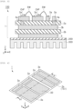
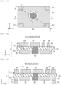
- FIG. 4 is a perspective view showing the insulating substrate 1
- FIG. 5 is a cross-sectional view taken along a line A1-A1 shown in FIG. 4
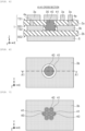
- FIGS. 6 and 7 are plan views showing a layer of the insulating substrate 1, a conductor 3b.
- the insulating substrate 1 includes a multilayer insulating substrate structure in which insulating plates and conductors through which a current flows are stacked for a plurality of layers.
- the insulating substrate 1 includes an insulating plate 2a, an insulating plate 2b, a plurality of conductors 3a, the conductor 3b, a plurality of connection conductors 4a, and a heat dissipation conductor 5.
- the insulating plate 2a includes a top surface TS1 and a back surface BS1. As shown in FIG. 4 , the plurality of conductors 3a are formed on the top surface TS1 of the insulating plate 2a. The plurality of conductors 3a include a non-connected conductor 30.
- the insulating plate 2b is formed on a back surface BS1 side of the insulating plate 2a and has a top surface TS2 and a back surface BS2.
- the conductor 3b is formed between the back surface BS1 of the insulating plate 2a and the top surface TS2 of the insulating plate 2b.
- the plurality of connection conductors 4a are formed in the insulating plate 2a in a manner of electrically connecting some of the plurality of conductors 3a and the conductor 3b.
- the heat dissipation conductor 5 electrically insulated from the conductor 3b is formed on the back surface BS2 of the insulating plate 2b.
- various electronic devices such as a plurality of semiconductor chips, capacitors, and inductors are disposed on the plurality of conductors 3a, and electrical conduction among the electronic devices is formed and a current path is constructed by electrically connecting the plurality of conductors 3a, the plurality of connection conductors 4a, and the conductor 3b.
- a case where one conductor 3b is provided is illustrated here.
- a plurality of conductors 3b may be provided. In this case, a more complicated circuit can be constructed by the plurality of conductors 3b.
- the insulating substrate 1 has a multilayer insulating substrate structure. Therefore, a distance between the plurality of semiconductor chips and the heat dissipation conductor 5 may increase, and heat dissipation may tend to deteriorate.
- the plurality of conductors 3a include the non-connected conductor 30 that is not electrically connected to the conductor 3b via the plurality of connection conductors 4a. Since a heat dissipation path electrically insulated from the current path is provided below the non-connected conductor 30, heat dissipation can be improved.
- a protruding conductor 40 is formed in the insulating plate 2a in a manner of being embedded in the insulating plate 2a and protruding from the back surface BS1 of the insulating plate 2a.
- the protruding conductor 40 is electrically connected to the non-connected conductor 30, and is electrically insulated from the heat dissipation conductor 5 by the insulating plate 2b.
- the protruding conductor 40 is electrically insulated from the conductor 3b by an insulating layer 41 surrounding the protruding conductor 40 in a plan view.
- the parasitic inductance Ls can be kept low, and heat dissipation can be improved.
- a plurality of protruding conductors 40 may be provided as shown in FIG. 7 instead of only one as shown in FIG 6 .
- the plurality of protruding conductors 40 are formed in the insulating plate 2a.
- Each of the plurality of protruding conductors 40 is electrically connected to the non-connected conductor 30, electrically insulated from the conductor 3b by the insulating layer 41, and electrically insulated from the heat dissipation conductor 5 by the insulating plate 2b.
- a planar area of each protruding conductor 40 is smaller than that in FIG. 6 , but heat dissipation can be ensured substantially the same in FIG. 7 as that in FIG. 6 when a total planar area of the plurality of protruding conductors 40 is designed to be substantially the same as that in FIG. 6 .
- the plurality of conductors 3a including the non-connected conductor 30, the conductor 3b, the heat dissipation conductor 5, the plurality of connection conductors 4a, and the protruding conductor 40 are made of, for example, a metal material containing copper (Cu) or aluminum (Al).
- the insulating plate 2a and the insulating plate 2b are made of, for example, a ceramic or resin material.
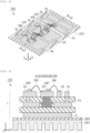
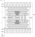
- FIG. 8 is a perspective view showing the power conversion apparatus 100
- FIGS. 9 and 10 are cross-sectional views taken along a line A2-A2 shown in FIG 8 .
- the line A2-A2 is located on the same straight line as the line A1-A1 shown in FIGS. 4 and 6 .
- the power conversion apparatus 100 includes the insulating substrate 1, a plurality of semiconductor chips CHP, bonding wires BW, a base plate 200 and a heat sink 300.
- the heat sink 300 is connected to the heat dissipation conductor 5 via the base plate 200.
- the heat dissipation conductor 5 and the base plate 200 are connected to each other via a thermal interface material (TIM).
- the base plate 200 and the heat sink 300 are also connected via a TIM.
- the TIM is, for example, a material such as solder or a sintered material.
- Each of the plurality of semiconductor chips CHP has a top surface and a back surface, and back surfaces of the plurality of semiconductor chips CHP are disposed on the plurality of conductors 3a by a TIM. At least one of the plurality of semiconductor chips CHP is provided on the non-connected conductor 30.
- the plurality of semiconductor chips CHP and the plurality of conductors 3a are electrically connected to each other by the bonding wires BW as appropriate.
- capacitors and inductors may be disposed on the plurality of conductors 3a.
- the insulating substrate 1, the plurality of semiconductor chips CHP, and the bonding wires BW may be covered with a protective member 400.
- the protective member 400 is made of an insulating material, and is made of, for example, an insulating gel or a molding resin.
- the semiconductor chip CHP includes, for example, a compound semiconductor substrate of silicon carbide (SiC), gallium nitride (GaN), gallium oxide (Ga 2 O 3 ), or the like, and a transistor such as a MOSFET formed on the compound semiconductor substrate.
- SiC silicon carbide
- GaN gallium nitride
- Ga 2 O 3 gallium oxide
- the bonding wire BW is made of, for example, a metal material containing gold (Au), copper (Cu), or aluminum (Al).
- the plurality of semiconductor chips CHP and the plurality of conductors 3a may be electrically connected by ribbons, bus bars, or the like instead of the bonding wires BW.
- the base plate 200 is made of, for example, a composite material (AlSiC) in which SiC ceramic particles are contained in copper (Cu) or an aluminum alloy, or a composite material (MgSiC) in which SiC ceramic particles are contained in magnesium.
- the heat sink 300 is made of, for example, a metal material containing copper (Cu), iron (Fe), or aluminum.
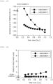
- FIGS. 11 and 12 are graphs showing effects according to Embodiment 1, and are simulation results measured by the inventors of the present application.
- FIGS. 11 and 12 also show effects according to Embodiment 3 described later.
- "Heat area” on a horizontal axis in FIGS. 11 and 12 indicates an area of the protruding conductor 40 in a plan view.
- a temperature rise can be prevented as compared with Study Example 2 ( FIG. 3 ), and the parasitic inductance Ls can be maintained to be substantially the same as that in Study Example 2 ( FIG. 3 ). That is, according to Embodiment 1, it is possible to provide the insulating substrate 1 capable of keeping the parasitic inductance Ls low and improving heat dissipation, and reliability of the power conversion apparatus 100 can be improved using such an insulating substrate 1.
- Embodiment 2 the insulating substrate 1 and the power conversion apparatus 100 according to Embodiment 2 will be described with reference to FIGS. 13 and 14 .
- differences from Embodiment 1 will be mainly described, and the description of points overlapping with Embodiment 1 will be omitted.
- the insulating substrate 1 according to Embodiment 2 has a multilayer insulating substrate structure in which more insulating plates and conductors are stacked between the insulating plate 2b and the heat dissipation conductor 5.
- an insulating plate 2c including a top surface TS3 and a back surface BS3 is formed between the insulating plate 2b and the heat dissipation conductor 5.
- a conductor 3c is formed between the back surface BS2 of the insulating plate 2b and the top surface TS3 of the insulating plate 2c.
- a plurality of connection conductors 4b are formed in the insulating plate 2b in a manner of electrically connecting the conductor 3b and the conductor 3c.
- the protruding conductor 40 penetrates the insulating plate 2b, protrudes from the back surface of the insulating plate 2b, and is electrically insulated from the conductor 3c and the connection conductors 4b.
- a structure including the insulating plate 2c, the conductor 3c, the plurality of connection conductors 4b, and the protruding conductor 40 is repeatedly formed once or more from the insulating plate 2b to the heat dissipation conductor 5.
- a conductor 3d, connection conductors 4c, and the like shown in FIG. 13 are formed.
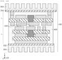
- FIG. 14 shows the power conversion apparatus 100 using the insulating substrate 1 according to Embodiment 2.
- the insulating substrate 1 that is further multi-layered, a plurality of semiconductor chips CHP, and the bonding wires BW may also be covered with the protective member 400.
- Various electronic devices such as the plurality of semiconductor chips CHP, capacitors, and inductors are disposed on a plurality of conductors 3a, but the insulating substrate 1 is further multi-layered. Therefore, it is easier to freely design connection paths of these electronic devices, and a degree of freedom in circuit design can be increased. It is also easier to freely design a current path that reduces the parasitic inductor Ls.
- Embodiment 3 the insulating substrate 1 and the power conversion apparatus 100 according to Embodiment 3 will be described with reference to FIGS. 15 to 18 .
- differences from Embodiment 1 will be mainly described, and the description of points overlapping with Embodiment 1 will be omitted.
- Embodiment 1 when the insulating substrate 1 has the multilayer insulating substrate structure, heat dissipation is improved by connecting the protruding conductor 40 to the non-connected conductor 30. In Embodiment 3, when the insulating substrate 1 has a single-layer insulating substrate structure, heat dissipation is improved by other devices.
- FIG. 15 is a plan view showing a layer of the insulating substrate 1, the conductors 3b, according to Embodiment 3.
- FIG. 16 is a cross-sectional view taken along the line A1-A1 shown in FIG. 15, and
- FIG. 17 is a cross-sectional view taken along a line B-B shown in FIG. 15 .
- a plurality of conductors 3a, the non-connected conductor 30, the insulating plate 2a, and the connection conductors 4a according to Embodiment 3 are the same as in Embodiment 1.
- the insulating plate 2b is not formed, and the protruding conductor 40 for connection to the non-connected conductor 30 is also not formed.
- a plurality of conductors 3b are formed, and the plurality of conductors 3b include non-connected conductors 31 electrically insulated from another conductor 3b.
- the non-connected conductors 31 are electrically insulated from the other conductor 3b and the connection conductors 4a.
- the non-connected conductors 31 are provided at four corners of the insulating substrate 1, but the number and positions of the non-connected conductors 31 can be changed as appropriate.
- the heat dissipation conductor 5 is connected to each of the plurality of non-connected conductors 31 in a manner of protruding from the other conductor 3b on a back surface BS1 side of the insulating plate 2a. That is, the heat dissipation conductor 5 is not connected to the conductor 3b other than the non-connected conductors 31. In other words, a total thickness of the non-connected conductor 31 and the heat dissipation conductor 5 is larger than a thickness of the conductor 3b other than the non-connected conductors 31.
- the conductor 3b other than the non-connected conductors 31 serves as a current path, and the non-connected conductor 31 and the heat dissipation conductor 5 constitute a heat dissipation path insulated from the current path.
- the connection conductors 4a may be provided at lower portions of some of the conductors 3a, and some of the conductors 3a and the non-connected conductors 31 may be connected to each other via the connection conductors 4a. Such a method can also improve heat dissipation.
- FIG. 18 shows the power conversion apparatus 100 using the insulating substrate 1 according to Embodiment 3.
- the heat dissipation conductors 5 are connected to the heat sink 300 via the base plate 200.
- the insulating substrate 1, a plurality of semiconductor chips CHP, and the bonding wires BW are also covered with the protective member 400.
- the protective member 400 is present between the conductor 3b serving as the current path and the non-connected conductors 31 and between the conductor 3b serving as the current path and the base plate 200, these members are electrically insulated.
- FIGS. 11 and 12 show the effects according to Embodiment 3.
- "Heat area” on the horizontal axis in FIGS. 11 and 12 indicates an area of the heat dissipation conductors 5 in a plan view (here, a total area of the four heat dissipation conductors 5).
- the parasitic inductance Ls is higher in Embodiment 3 than in Study Example 2 ( FIG. 3 ), but the parasitic inductance Ls is substantially the same in Embodiment 3 as that in Study Example 1 ( FIG. 1 ), which has a single-layer insulating substrate structure.
- Embodiment 3 can also provide the insulating substrate 1 capable of keeping the parasitic inductance Ls low and improving heat dissipation, and reliability of the power conversion apparatus 100 can be improved using such an insulating substrate 1.
- Embodiment 4 the insulating substrate 1 and the power conversion apparatus 100 according to Embodiment 4 will be described with reference to FIGS. 19 to 22 .
- differences from Embodiment 3 will be mainly described, and the description of points overlapping with Embodiment 3 will be omitted.
- the protruding conductor 40 described in Embodiment 1 is applied based on the insulating substrate 1 according to Embodiment 3.
- FIG. 19 is a plan view showing a layer of the insulating substrate 1, the conductors 3b, according to Embodiment 4.
- FIG. 20 is a cross-sectional view taken along the line A1-A1 shown in FIG. 19, and
- FIG. 21 is a cross-sectional view taken along the line B-B shown in FIG. 19 .
- the protruding conductor 40 is formed in the insulating plate 2a in a manner of being embedded in the insulating plate 2a and protruding from the back surface BS1 of the insulating plate 2a.
- the protruding conductor 40 is electrically connected to the non-connected conductor 30, and is electrically insulated from the conductor 3b, the non-connected conductors 31, and the heat dissipation conductors 5.
- a plurality of protruding conductors 40 as shown in FIG. 7 can be also applied in Embodiment 4.
- FIG. 22 shows the power conversion apparatus 100 using the insulating substrate 1 according to Embodiment 4.
- the heat dissipation conductors 5 are connected to the heat sink 300 via the base plate 200.
- the insulating substrate 1, a plurality of semiconductor chips CHP, and the bonding wires BW are also covered with the protective member 400.
- the protective member 400 is present between the protruding conductor 40 and the conductor 3b serving as a current path and between the protruding conductor 40 and the base plate 200, these members are electrically insulated.
- the protruding conductor 40 according to Embodiment 4 protrudes toward the base plate 200 to the same extent as the conductor 3b, the protruding conductor 40 only needs to protrude to such an extent that the protruding conductor 40 does not contact the base plate 200.
- Embodiment 4 substantially the same effects as those according to Embodiment 3 can be attained, and heat dissipation can be further improved due to presence of the protruding conductor 40. Therefore, reliability of the power conversion apparatus 100 can be further improved.
- the insulating substrate 1 is mounted only on back surfaces of the semiconductor chips CHP in the power conversion apparatus 100 according to Embodiments 1 to 4. Alternatively, the insulating substrate 1 may be mounted on top surfaces of semiconductor chips CHP as well.
- one insulating substrate 1 and the other insulating substrate 1 are arranged such that a plurality of conductors 3a face each other.
- Back surfaces of a plurality of semiconductor chips CHP are disposed on a plurality of conductors 3a of the one insulating substrate 1
- top surfaces of the plurality of semiconductor chips CHP are disposed on a plurality of conductors 3a of the other insulating substrate 1.
- at least one of the plurality of semiconductor chips CHP is provided on the non-connected conductor 30 of the one insulating substrate 1 and on the non-connected conductor 30 of the other insulating substrate 1.
- Each of the heat dissipation conductor 5 of the one insulating substrate 1 and the heat dissipation conductor 5 of the other insulating substrate 1 is connected to a respective one of the heat sinks 300 via the base plate 200.
- Two sets of insulating substrates 1 and the plurality of semiconductor chips CHP are covered with the protective member 400.
- the parasitic inductance Ls can be reduced even in a structure in which both surfaces of each of the semiconductor chips CHP are sandwiched by the two sets of insulating substrates 1. Since heat can be dissipated from both surfaces of each of the semiconductor chips CHP, heat dissipation can be further improved. Therefore, reliability of the power conversion apparatus 100 can be improved.
- the two sets of insulating substrates 1 may not have the same structure.
- a structure according to Embodiment 1 may be applied to the one insulating substrate 1
- a structure according to Embodiment 4 may be applied to the other insulating substrate 1.
- a combination of the two sets of insulating substrates 1 can be selected from structures according to Embodiments 1 to 4 as appropriate.
- the base plates 200 and the heat sinks 300 may not necessarily be provided when an amount of heat dissipation is sufficient.
Landscapes
- Engineering & Computer Science (AREA)
- Microelectronics & Electronic Packaging (AREA)
- Power Engineering (AREA)
- General Physics & Mathematics (AREA)
- Physics & Mathematics (AREA)
- Condensed Matter Physics & Semiconductors (AREA)
- Computer Hardware Design (AREA)
- Chemical & Material Sciences (AREA)
- Materials Engineering (AREA)
- Ceramic Engineering (AREA)
- Structure Of Printed Boards (AREA)
- Inverter Devices (AREA)
- Cooling Or The Like Of Semiconductors Or Solid State Devices (AREA)
Applications Claiming Priority (2)
| Application Number | Priority Date | Filing Date | Title |
|---|---|---|---|
| JP2020200810A JP2022088783A (ja) | 2020-12-03 | 2020-12-03 | 絶縁基板および電力変換装置 |
| PCT/JP2021/032188 WO2022118510A1 (ja) | 2020-12-03 | 2021-09-01 | 絶縁基板および電力変換装置 |
Publications (1)
| Publication Number | Publication Date |
|---|---|
| EP4258337A1 true EP4258337A1 (en) | 2023-10-11 |
Family
ID=81852691
Family Applications (1)
| Application Number | Title | Priority Date | Filing Date |
|---|---|---|---|
| EP21900266.4A Pending EP4258337A1 (en) | 2020-12-03 | 2021-09-01 | Insulated board and power converter |
Country Status (3)
| Country | Link |
|---|---|
| EP (1) | EP4258337A1 (ja) |
| JP (1) | JP2022088783A (ja) |
| WO (1) | WO2022118510A1 (ja) |
Family Cites Families (5)
| Publication number | Priority date | Publication date | Assignee | Title |
|---|---|---|---|---|
| JP5250707B2 (ja) * | 2011-05-26 | 2013-07-31 | 有限会社 ナプラ | 電子機器用基板及び電子機器 |
| JP6004094B2 (ja) * | 2013-04-24 | 2016-10-05 | 富士電機株式会社 | パワー半導体モジュールおよびその製造方法、電力変換器 |
| JP5975180B2 (ja) * | 2013-10-03 | 2016-08-23 | 富士電機株式会社 | 半導体モジュール |
| JP6331543B2 (ja) * | 2014-03-24 | 2018-05-30 | 日産自動車株式会社 | ハーフブリッジパワー半導体モジュール及びその製造方法 |
| JP2019046899A (ja) * | 2017-08-31 | 2019-03-22 | ルネサスエレクトロニクス株式会社 | 電子装置 |
-
2020
- 2020-12-03 JP JP2020200810A patent/JP2022088783A/ja active Pending
-
2021
- 2021-09-01 WO PCT/JP2021/032188 patent/WO2022118510A1/ja unknown
- 2021-09-01 EP EP21900266.4A patent/EP4258337A1/en active Pending
Also Published As
| Publication number | Publication date |
|---|---|
| WO2022118510A1 (ja) | 2022-06-09 |
| JP2022088783A (ja) | 2022-06-15 |
Similar Documents
| Publication | Publication Date | Title |
|---|---|---|
| US10638633B2 (en) | Power module, power converter and manufacturing method of power module | |
| US7786486B2 (en) | Double-sided package for power module | |
| US20220208643A1 (en) | Electronic circuit and method for producing an electronic circuit | |
| Dietrich | Trends in automotive power semiconductor packaging | |
| US9385107B2 (en) | Multichip device including a substrate | |
| JP2007234690A (ja) | パワー半導体モジュール | |
| EP2889902B1 (en) | Electric power semiconductor device | |
| US10079195B2 (en) | Semiconductor chip package comprising laterally extending connectors | |
| JP2010283053A (ja) | 半導体装置及びその製造方法 | |
| EP4128341A1 (en) | Multi-chip package with reinforced isolation | |
| CN113228265A (zh) | 半导体组件的电路构造 | |
| WO2012081434A1 (ja) | 半導体装置 | |
| US11942449B2 (en) | Semiconductor arrangement and method for producing the same | |
| EP3958305A1 (en) | Power semiconductor module arrangement and method for producing the same | |
| CN112530915A (zh) | 半导体装置 | |
| EP4258337A1 (en) | Insulated board and power converter | |
| US11527456B2 (en) | Power module with organic layers | |
| CN117043936A (zh) | 具有一体式散热器的电子封装 | |
| WO2022213013A1 (en) | Double-side cooled power modules with sintered-silver interposers | |
| CN111584422B (zh) | 半导体装置及其制造方法 | |
| Bäumler et al. | Reliability aspects of 3D integrated power devices | |
| JP2009064904A (ja) | 銅回路基板およびこれを用いた半導体モジュール装置 | |
| EP4084062A1 (en) | Power semiconductor module arrangement | |
| US11521921B2 (en) | Semiconductor device package assemblies and methods of manufacture | |
| CN110299340B (zh) | 半导体装置 |
Legal Events
| Date | Code | Title | Description |
|---|---|---|---|
| STAA | Information on the status of an ep patent application or granted ep patent |
Free format text: STATUS: THE INTERNATIONAL PUBLICATION HAS BEEN MADE |
|
| PUAI | Public reference made under article 153(3) epc to a published international application that has entered the european phase |
Free format text: ORIGINAL CODE: 0009012 |
|
| STAA | Information on the status of an ep patent application or granted ep patent |
Free format text: STATUS: REQUEST FOR EXAMINATION WAS MADE |
|
| 17P | Request for examination filed |
Effective date: 20230703 |
|
| AK | Designated contracting states |
Kind code of ref document: A1 Designated state(s): AL AT BE BG CH CY CZ DE DK EE ES FI FR GB GR HR HU IE IS IT LI LT LU LV MC MK MT NL NO PL PT RO RS SE SI SK SM TR |
|
| DAV | Request for validation of the european patent (deleted) | ||
| DAX | Request for extension of the european patent (deleted) |