EP4258337A1 - Isolierte leiterplatte und stromwandler - Google Patents
Isolierte leiterplatte und stromwandler Download PDFInfo
- Publication number
- EP4258337A1 EP4258337A1 EP21900266.4A EP21900266A EP4258337A1 EP 4258337 A1 EP4258337 A1 EP 4258337A1 EP 21900266 A EP21900266 A EP 21900266A EP 4258337 A1 EP4258337 A1 EP 4258337A1
- Authority
- EP
- European Patent Office
- Prior art keywords
- conductor
- conductors
- insulating plate
- insulating
- insulating substrate
- Prior art date
- Legal status (The legal status is an assumption and is not a legal conclusion. Google has not performed a legal analysis and makes no representation as to the accuracy of the status listed.)
- Granted
Links
Images


Classifications
-
- H—ELECTRICITY
- H10—SEMICONDUCTOR DEVICES; ELECTRIC SOLID-STATE DEVICES NOT OTHERWISE PROVIDED FOR
- H10W—GENERIC PACKAGES, INTERCONNECTIONS, CONNECTORS OR OTHER CONSTRUCTIONAL DETAILS OF DEVICES COVERED BY CLASS H10
- H10W40/00—Arrangements for thermal protection or thermal control
- H10W40/20—Arrangements for cooling
- H10W40/25—Arrangements for cooling characterised by their materials
- H10W40/255—Arrangements for cooling characterised by their materials having a laminate or multilayered structure, e.g. direct bond copper [DBC] ceramic substrates
-
- H—ELECTRICITY
- H10—SEMICONDUCTOR DEVICES; ELECTRIC SOLID-STATE DEVICES NOT OTHERWISE PROVIDED FOR
- H10W—GENERIC PACKAGES, INTERCONNECTIONS, CONNECTORS OR OTHER CONSTRUCTIONAL DETAILS OF DEVICES COVERED BY CLASS H10
- H10W40/00—Arrangements for thermal protection or thermal control
- H10W40/20—Arrangements for cooling
- H10W40/22—Arrangements for cooling characterised by their shape, e.g. having conical or cylindrical projections
- H10W40/226—Arrangements for cooling characterised by their shape, e.g. having conical or cylindrical projections characterised by projecting parts, e.g. fins to increase surface area
- H10W40/228—Arrangements for cooling characterised by their shape, e.g. having conical or cylindrical projections characterised by projecting parts, e.g. fins to increase surface area the projecting parts being wire-shaped or pin-shaped
-
- H—ELECTRICITY
- H10—SEMICONDUCTOR DEVICES; ELECTRIC SOLID-STATE DEVICES NOT OTHERWISE PROVIDED FOR
- H10W—GENERIC PACKAGES, INTERCONNECTIONS, CONNECTORS OR OTHER CONSTRUCTIONAL DETAILS OF DEVICES COVERED BY CLASS H10
- H10W44/00—Electrical arrangements for controlling or matching impedance
- H10W44/501—Inductive arrangements
-
- H—ELECTRICITY
- H10—SEMICONDUCTOR DEVICES; ELECTRIC SOLID-STATE DEVICES NOT OTHERWISE PROVIDED FOR
- H10W—GENERIC PACKAGES, INTERCONNECTIONS, CONNECTORS OR OTHER CONSTRUCTIONAL DETAILS OF DEVICES COVERED BY CLASS H10
- H10W90/00—Package configurations
-
- H—ELECTRICITY
- H02—GENERATION; CONVERSION OR DISTRIBUTION OF ELECTRIC POWER
- H02M—APPARATUS FOR CONVERSION BETWEEN AC AND AC, BETWEEN AC AND DC, OR BETWEEN DC AND DC, AND FOR USE WITH MAINS OR SIMILAR POWER SUPPLY SYSTEMS; CONVERSION OF DC OR AC INPUT POWER INTO SURGE OUTPUT POWER; CONTROL OR REGULATION THEREOF
- H02M1/00—Details of apparatus for conversion
- H02M1/32—Means for protecting converters other than automatic disconnection
- H02M1/327—Means for protecting converters other than automatic disconnection against abnormal temperatures
-
- H—ELECTRICITY
- H02—GENERATION; CONVERSION OR DISTRIBUTION OF ELECTRIC POWER
- H02M—APPARATUS FOR CONVERSION BETWEEN AC AND AC, BETWEEN AC AND DC, OR BETWEEN DC AND DC, AND FOR USE WITH MAINS OR SIMILAR POWER SUPPLY SYSTEMS; CONVERSION OF DC OR AC INPUT POWER INTO SURGE OUTPUT POWER; CONTROL OR REGULATION THEREOF
- H02M7/00—Conversion of AC power input into DC power output; Conversion of DC power input into AC power output
- H02M7/003—Constructional details, e.g. physical layout, assembly, wiring or busbar connections
-
- H—ELECTRICITY
- H10—SEMICONDUCTOR DEVICES; ELECTRIC SOLID-STATE DEVICES NOT OTHERWISE PROVIDED FOR
- H10W—GENERIC PACKAGES, INTERCONNECTIONS, CONNECTORS OR OTHER CONSTRUCTIONAL DETAILS OF DEVICES COVERED BY CLASS H10
- H10W70/00—Package substrates; Interposers; Redistribution layers [RDL]
- H10W70/60—Insulating or insulated package substrates; Interposers; Redistribution layers
- H10W70/611—Insulating or insulated package substrates; Interposers; Redistribution layers for connecting multiple chips together
-
- H—ELECTRICITY
- H10—SEMICONDUCTOR DEVICES; ELECTRIC SOLID-STATE DEVICES NOT OTHERWISE PROVIDED FOR
- H10W—GENERIC PACKAGES, INTERCONNECTIONS, CONNECTORS OR OTHER CONSTRUCTIONAL DETAILS OF DEVICES COVERED BY CLASS H10
- H10W70/00—Package substrates; Interposers; Redistribution layers [RDL]
- H10W70/60—Insulating or insulated package substrates; Interposers; Redistribution layers
- H10W70/62—Insulating or insulated package substrates; Interposers; Redistribution layers characterised by their interconnections
- H10W70/65—Shapes or dispositions of interconnections
-
- H—ELECTRICITY
- H10—SEMICONDUCTOR DEVICES; ELECTRIC SOLID-STATE DEVICES NOT OTHERWISE PROVIDED FOR
- H10W—GENERIC PACKAGES, INTERCONNECTIONS, CONNECTORS OR OTHER CONSTRUCTIONAL DETAILS OF DEVICES COVERED BY CLASS H10
- H10W72/00—Interconnections or connectors in packages
- H10W72/50—Bond wires
- H10W72/531—Shapes of wire connectors
- H10W72/5363—Shapes of wire connectors the connected ends being wedge-shaped
-
- H—ELECTRICITY
- H10—SEMICONDUCTOR DEVICES; ELECTRIC SOLID-STATE DEVICES NOT OTHERWISE PROVIDED FOR
- H10W—GENERIC PACKAGES, INTERCONNECTIONS, CONNECTORS OR OTHER CONSTRUCTIONAL DETAILS OF DEVICES COVERED BY CLASS H10
- H10W74/00—Encapsulations, e.g. protective coatings
-
- H—ELECTRICITY
- H10—SEMICONDUCTOR DEVICES; ELECTRIC SOLID-STATE DEVICES NOT OTHERWISE PROVIDED FOR
- H10W—GENERIC PACKAGES, INTERCONNECTIONS, CONNECTORS OR OTHER CONSTRUCTIONAL DETAILS OF DEVICES COVERED BY CLASS H10
- H10W74/00—Encapsulations, e.g. protective coatings
- H10W74/10—Encapsulations, e.g. protective coatings characterised by their shape or disposition
- H10W74/111—Encapsulations, e.g. protective coatings characterised by their shape or disposition the semiconductor body being completely enclosed
- H10W74/114—Encapsulations, e.g. protective coatings characterised by their shape or disposition the semiconductor body being completely enclosed by a substrate and the encapsulations
-
- H—ELECTRICITY
- H10—SEMICONDUCTOR DEVICES; ELECTRIC SOLID-STATE DEVICES NOT OTHERWISE PROVIDED FOR
- H10W—GENERIC PACKAGES, INTERCONNECTIONS, CONNECTORS OR OTHER CONSTRUCTIONAL DETAILS OF DEVICES COVERED BY CLASS H10
- H10W76/00—Containers; Fillings or auxiliary members therefor; Seals
- H10W76/10—Containers or parts thereof
- H10W76/12—Containers or parts thereof characterised by their shape
- H10W76/13—Containers comprising a conductive base serving as an interconnection
- H10W76/138—Containers comprising a conductive base serving as an interconnection having another interconnection being formed by a cover plate parallel to the conductive base, e.g. sandwich type
-
- H—ELECTRICITY
- H10—SEMICONDUCTOR DEVICES; ELECTRIC SOLID-STATE DEVICES NOT OTHERWISE PROVIDED FOR
- H10W—GENERIC PACKAGES, INTERCONNECTIONS, CONNECTORS OR OTHER CONSTRUCTIONAL DETAILS OF DEVICES COVERED BY CLASS H10
- H10W90/00—Package configurations
- H10W90/701—Package configurations characterised by the relative positions of pads or connectors relative to package parts
- H10W90/751—Package configurations characterised by the relative positions of pads or connectors relative to package parts of bond wires
- H10W90/754—Package configurations characterised by the relative positions of pads or connectors relative to package parts of bond wires between a chip and a stacked insulating package substrate, interposer or RDL
Definitions
- the present invention relates to an insulating substrate and a power conversion apparatus, and more particularly to an insulating substrate for mounting a semiconductor chip and a power conversion apparatus using the insulating substrate.
- the power semiconductor chip of SiC, GaN, or the like can be driven at a high frequency, passive components such as inductors or capacitors provided in the power conversion apparatus can be downsized. With these effects, it is possible to reduce an overall size of the power conversion apparatus.
- a parasitic inductance Ls of the power conversion apparatus becomes a problem during high-frequency driving.
- a surge voltage ⁇ V is represented by a product of the parasitic inductance Ls and an amount of current per time unit (di/dt).
- the large parasitic inductance Ls causes the large surge voltage ⁇ V to be applied when the semiconductor chip is turned off, and also becomes a source of noise.
- the surge voltage ⁇ V and the noise greatly affect the off-speed.
- PTL 1 discloses an insulating substrate including an insulating plate, a top surface wiring conductor formed on a top surface of the insulating plate, and a back surface wiring conductor formed on a back surface of the insulating plate.
- a semiconductor chip is disposed on the top surface wiring conductor.
- PTL 1 discloses a technique for reducing a parasitic inductance using a bridge terminal provided on the top surface wiring conductor due to an effect of proximity reverse conduction.
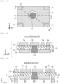
- the inventors of the present application have studied structures according to Study Example 1 shown in FIG. 2 and Study Example 2 shown in FIG. 3 as power conversion apparatus 100 for compound semiconductor substrates.
- the power conversion apparatus 100 uses an insulating substrate 1 including an insulating plate 2a, a plurality of conductors 3a formed on a top surface of the insulating plate 2a, and a heat dissipation conductor 5 formed on a back surface of the insulating plate 2a.
- a plurality of semiconductor chips CHP are disposed on the plurality of conductors 3a, and the plurality of conductors 3a and the plurality of semiconductor chips CHP are electrically connected by bonding wires BW as appropriate.
- the heat dissipation conductor 5 is connected to a heat sink 300 via a base plate 200.
- the power conversion apparatus 100 according to Study Example 2 further includes a conductor 3b and an insulating plate 2b between the insulating plate 2a and the heat dissipation conductor 5, thereby forming a multilayer insulating substrate structure.
- the parasitic inductance Ls can be reduced by mutual inductance as compared with Study Example 1.
- an insulating substrate including: a first insulating plate including a top surface and a back surface; a second insulating plate formed on a back surface side of the first insulating plate and including a top surface and a back surface; a plurality of first conductors formed on the top surface of the first insulating plate; a second conductor formed between the back surface of the first insulating plate and the top surface of the second insulating plate; a heat dissipation conductor formed on the back surface of the second insulating plate and electrically insulated from the second conductor; and a plurality of first connection conductors formed inside the first insulating plate in a manner of electrically connecting some of the plurality of first conductors and the second conductor.
- the plurality of first conductors include a first non-connected conductor that is not electrically connected to the second conductor via the plurality of first connection conductors, a protruding conductor is formed in the first insulating plate in a manner of being embedded in the first insulating plate and protruding from the back surface of the first insulating plate, and the protruding conductor is electrically connected to the first non-connected conductor, and is electrically insulated from the second conductor and the heat dissipation conductor.
- an insulating substrate including: a first insulating plate including a top surface and a back surface; a plurality of first conductors formed on the top surface of the first insulating plate; a plurality of second conductors formed on the back surface of the first insulating plate; and a plurality of first connection conductors formed inside the first insulating plate in a manner of electrically connecting some of the plurality of first conductors and some of the plurality of second conductors.
- the plurality of second conductors include a second non-connected conductor electrically insulated from another second conductor, and a heat dissipation conductor is connected to the second non-connected conductor in a manner of protruding from the other second conductor on a back surface side of the first insulating plate.
- an insulating substrate capable of keeping a parasitic inductance low and improving heat dissipation. Reliability of a power conversion apparatus can be improved using such an insulating substrate.
- An X direction, a Y direction, and a Z direction described in the present application intersect with one another and are orthogonal to one another.
- the Z direction is referred to as a vertical direction, an upper-lower direction, a height direction, or a thickness direction of a certain structure.
- An expression "plan view" used in the present application means viewing a plane formed by the X direction and the Y direction from the Z direction.
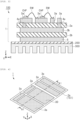
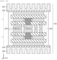
- FIG. 4 is a perspective view showing the insulating substrate 1
- FIG. 5 is a cross-sectional view taken along a line A1-A1 shown in FIG. 4
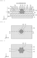
- FIGS. 6 and 7 are plan views showing a layer of the insulating substrate 1, a conductor 3b.
- the insulating substrate 1 includes a multilayer insulating substrate structure in which insulating plates and conductors through which a current flows are stacked for a plurality of layers.
- the insulating substrate 1 includes an insulating plate 2a, an insulating plate 2b, a plurality of conductors 3a, the conductor 3b, a plurality of connection conductors 4a, and a heat dissipation conductor 5.
- the insulating plate 2a includes a top surface TS1 and a back surface BS1. As shown in FIG. 4 , the plurality of conductors 3a are formed on the top surface TS1 of the insulating plate 2a. The plurality of conductors 3a include a non-connected conductor 30.
- the insulating plate 2b is formed on a back surface BS1 side of the insulating plate 2a and has a top surface TS2 and a back surface BS2.
- the conductor 3b is formed between the back surface BS1 of the insulating plate 2a and the top surface TS2 of the insulating plate 2b.
- the plurality of connection conductors 4a are formed in the insulating plate 2a in a manner of electrically connecting some of the plurality of conductors 3a and the conductor 3b.
- the heat dissipation conductor 5 electrically insulated from the conductor 3b is formed on the back surface BS2 of the insulating plate 2b.
- various electronic devices such as a plurality of semiconductor chips, capacitors, and inductors are disposed on the plurality of conductors 3a, and electrical conduction among the electronic devices is formed and a current path is constructed by electrically connecting the plurality of conductors 3a, the plurality of connection conductors 4a, and the conductor 3b.
- a case where one conductor 3b is provided is illustrated here.
- a plurality of conductors 3b may be provided. In this case, a more complicated circuit can be constructed by the plurality of conductors 3b.
- the insulating substrate 1 has a multilayer insulating substrate structure. Therefore, a distance between the plurality of semiconductor chips and the heat dissipation conductor 5 may increase, and heat dissipation may tend to deteriorate.
- the plurality of conductors 3a include the non-connected conductor 30 that is not electrically connected to the conductor 3b via the plurality of connection conductors 4a. Since a heat dissipation path electrically insulated from the current path is provided below the non-connected conductor 30, heat dissipation can be improved.
- a protruding conductor 40 is formed in the insulating plate 2a in a manner of being embedded in the insulating plate 2a and protruding from the back surface BS1 of the insulating plate 2a.
- the protruding conductor 40 is electrically connected to the non-connected conductor 30, and is electrically insulated from the heat dissipation conductor 5 by the insulating plate 2b.
- the protruding conductor 40 is electrically insulated from the conductor 3b by an insulating layer 41 surrounding the protruding conductor 40 in a plan view.
- the parasitic inductance Ls can be kept low, and heat dissipation can be improved.
- a plurality of protruding conductors 40 may be provided as shown in FIG. 7 instead of only one as shown in FIG 6 .
- the plurality of protruding conductors 40 are formed in the insulating plate 2a.
- Each of the plurality of protruding conductors 40 is electrically connected to the non-connected conductor 30, electrically insulated from the conductor 3b by the insulating layer 41, and electrically insulated from the heat dissipation conductor 5 by the insulating plate 2b.
- a planar area of each protruding conductor 40 is smaller than that in FIG. 6 , but heat dissipation can be ensured substantially the same in FIG. 7 as that in FIG. 6 when a total planar area of the plurality of protruding conductors 40 is designed to be substantially the same as that in FIG. 6 .
- the plurality of conductors 3a including the non-connected conductor 30, the conductor 3b, the heat dissipation conductor 5, the plurality of connection conductors 4a, and the protruding conductor 40 are made of, for example, a metal material containing copper (Cu) or aluminum (Al).
- the insulating plate 2a and the insulating plate 2b are made of, for example, a ceramic or resin material.
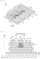
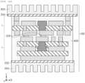
- FIG. 8 is a perspective view showing the power conversion apparatus 100
- FIGS. 9 and 10 are cross-sectional views taken along a line A2-A2 shown in FIG 8 .
- the line A2-A2 is located on the same straight line as the line A1-A1 shown in FIGS. 4 and 6 .
- the power conversion apparatus 100 includes the insulating substrate 1, a plurality of semiconductor chips CHP, bonding wires BW, a base plate 200 and a heat sink 300.
- the heat sink 300 is connected to the heat dissipation conductor 5 via the base plate 200.
- the heat dissipation conductor 5 and the base plate 200 are connected to each other via a thermal interface material (TIM).
- the base plate 200 and the heat sink 300 are also connected via a TIM.
- the TIM is, for example, a material such as solder or a sintered material.
- Each of the plurality of semiconductor chips CHP has a top surface and a back surface, and back surfaces of the plurality of semiconductor chips CHP are disposed on the plurality of conductors 3a by a TIM. At least one of the plurality of semiconductor chips CHP is provided on the non-connected conductor 30.
- the plurality of semiconductor chips CHP and the plurality of conductors 3a are electrically connected to each other by the bonding wires BW as appropriate.
- capacitors and inductors may be disposed on the plurality of conductors 3a.
- the insulating substrate 1, the plurality of semiconductor chips CHP, and the bonding wires BW may be covered with a protective member 400.
- the protective member 400 is made of an insulating material, and is made of, for example, an insulating gel or a molding resin.
- the semiconductor chip CHP includes, for example, a compound semiconductor substrate of silicon carbide (SiC), gallium nitride (GaN), gallium oxide (Ga 2 O 3 ), or the like, and a transistor such as a MOSFET formed on the compound semiconductor substrate.
- SiC silicon carbide
- GaN gallium nitride
- Ga 2 O 3 gallium oxide
- the bonding wire BW is made of, for example, a metal material containing gold (Au), copper (Cu), or aluminum (Al).
- the plurality of semiconductor chips CHP and the plurality of conductors 3a may be electrically connected by ribbons, bus bars, or the like instead of the bonding wires BW.
- the base plate 200 is made of, for example, a composite material (AlSiC) in which SiC ceramic particles are contained in copper (Cu) or an aluminum alloy, or a composite material (MgSiC) in which SiC ceramic particles are contained in magnesium.
- the heat sink 300 is made of, for example, a metal material containing copper (Cu), iron (Fe), or aluminum.
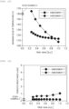
- FIGS. 11 and 12 are graphs showing effects according to Embodiment 1, and are simulation results measured by the inventors of the present application.
- FIGS. 11 and 12 also show effects according to Embodiment 3 described later.
- "Heat area” on a horizontal axis in FIGS. 11 and 12 indicates an area of the protruding conductor 40 in a plan view.
- a temperature rise can be prevented as compared with Study Example 2 ( FIG. 3 ), and the parasitic inductance Ls can be maintained to be substantially the same as that in Study Example 2 ( FIG. 3 ). That is, according to Embodiment 1, it is possible to provide the insulating substrate 1 capable of keeping the parasitic inductance Ls low and improving heat dissipation, and reliability of the power conversion apparatus 100 can be improved using such an insulating substrate 1.
- Embodiment 2 the insulating substrate 1 and the power conversion apparatus 100 according to Embodiment 2 will be described with reference to FIGS. 13 and 14 .
- differences from Embodiment 1 will be mainly described, and the description of points overlapping with Embodiment 1 will be omitted.
- the insulating substrate 1 according to Embodiment 2 has a multilayer insulating substrate structure in which more insulating plates and conductors are stacked between the insulating plate 2b and the heat dissipation conductor 5.
- an insulating plate 2c including a top surface TS3 and a back surface BS3 is formed between the insulating plate 2b and the heat dissipation conductor 5.
- a conductor 3c is formed between the back surface BS2 of the insulating plate 2b and the top surface TS3 of the insulating plate 2c.
- a plurality of connection conductors 4b are formed in the insulating plate 2b in a manner of electrically connecting the conductor 3b and the conductor 3c.
- the protruding conductor 40 penetrates the insulating plate 2b, protrudes from the back surface of the insulating plate 2b, and is electrically insulated from the conductor 3c and the connection conductors 4b.
- a structure including the insulating plate 2c, the conductor 3c, the plurality of connection conductors 4b, and the protruding conductor 40 is repeatedly formed once or more from the insulating plate 2b to the heat dissipation conductor 5.
- a conductor 3d, connection conductors 4c, and the like shown in FIG. 13 are formed.
- FIG. 14 shows the power conversion apparatus 100 using the insulating substrate 1 according to Embodiment 2.
- the insulating substrate 1 that is further multi-layered, a plurality of semiconductor chips CHP, and the bonding wires BW may also be covered with the protective member 400.
- Various electronic devices such as the plurality of semiconductor chips CHP, capacitors, and inductors are disposed on a plurality of conductors 3a, but the insulating substrate 1 is further multi-layered. Therefore, it is easier to freely design connection paths of these electronic devices, and a degree of freedom in circuit design can be increased. It is also easier to freely design a current path that reduces the parasitic inductor Ls.
- Embodiment 3 the insulating substrate 1 and the power conversion apparatus 100 according to Embodiment 3 will be described with reference to FIGS. 15 to 18 .
- differences from Embodiment 1 will be mainly described, and the description of points overlapping with Embodiment 1 will be omitted.
- Embodiment 1 when the insulating substrate 1 has the multilayer insulating substrate structure, heat dissipation is improved by connecting the protruding conductor 40 to the non-connected conductor 30. In Embodiment 3, when the insulating substrate 1 has a single-layer insulating substrate structure, heat dissipation is improved by other devices.
- FIG. 15 is a plan view showing a layer of the insulating substrate 1, the conductors 3b, according to Embodiment 3.
- FIG. 16 is a cross-sectional view taken along the line A1-A1 shown in FIG. 15, and
- FIG. 17 is a cross-sectional view taken along a line B-B shown in FIG. 15 .
- a plurality of conductors 3a, the non-connected conductor 30, the insulating plate 2a, and the connection conductors 4a according to Embodiment 3 are the same as in Embodiment 1.
- the insulating plate 2b is not formed, and the protruding conductor 40 for connection to the non-connected conductor 30 is also not formed.
- a plurality of conductors 3b are formed, and the plurality of conductors 3b include non-connected conductors 31 electrically insulated from another conductor 3b.
- the non-connected conductors 31 are electrically insulated from the other conductor 3b and the connection conductors 4a.
- the non-connected conductors 31 are provided at four corners of the insulating substrate 1, but the number and positions of the non-connected conductors 31 can be changed as appropriate.
- the heat dissipation conductor 5 is connected to each of the plurality of non-connected conductors 31 in a manner of protruding from the other conductor 3b on a back surface BS1 side of the insulating plate 2a. That is, the heat dissipation conductor 5 is not connected to the conductor 3b other than the non-connected conductors 31. In other words, a total thickness of the non-connected conductor 31 and the heat dissipation conductor 5 is larger than a thickness of the conductor 3b other than the non-connected conductors 31.
- the conductor 3b other than the non-connected conductors 31 serves as a current path, and the non-connected conductor 31 and the heat dissipation conductor 5 constitute a heat dissipation path insulated from the current path.
- the connection conductors 4a may be provided at lower portions of some of the conductors 3a, and some of the conductors 3a and the non-connected conductors 31 may be connected to each other via the connection conductors 4a. Such a method can also improve heat dissipation.
- FIG. 18 shows the power conversion apparatus 100 using the insulating substrate 1 according to Embodiment 3.
- the heat dissipation conductors 5 are connected to the heat sink 300 via the base plate 200.
- the insulating substrate 1, a plurality of semiconductor chips CHP, and the bonding wires BW are also covered with the protective member 400.
- the protective member 400 is present between the conductor 3b serving as the current path and the non-connected conductors 31 and between the conductor 3b serving as the current path and the base plate 200, these members are electrically insulated.
- FIGS. 11 and 12 show the effects according to Embodiment 3.
- "Heat area” on the horizontal axis in FIGS. 11 and 12 indicates an area of the heat dissipation conductors 5 in a plan view (here, a total area of the four heat dissipation conductors 5).
- the parasitic inductance Ls is higher in Embodiment 3 than in Study Example 2 ( FIG. 3 ), but the parasitic inductance Ls is substantially the same in Embodiment 3 as that in Study Example 1 ( FIG. 1 ), which has a single-layer insulating substrate structure.
- Embodiment 3 can also provide the insulating substrate 1 capable of keeping the parasitic inductance Ls low and improving heat dissipation, and reliability of the power conversion apparatus 100 can be improved using such an insulating substrate 1.
- Embodiment 4 the insulating substrate 1 and the power conversion apparatus 100 according to Embodiment 4 will be described with reference to FIGS. 19 to 22 .
- differences from Embodiment 3 will be mainly described, and the description of points overlapping with Embodiment 3 will be omitted.
- the protruding conductor 40 described in Embodiment 1 is applied based on the insulating substrate 1 according to Embodiment 3.
- FIG. 19 is a plan view showing a layer of the insulating substrate 1, the conductors 3b, according to Embodiment 4.
- FIG. 20 is a cross-sectional view taken along the line A1-A1 shown in FIG. 19, and
- FIG. 21 is a cross-sectional view taken along the line B-B shown in FIG. 19 .
- the protruding conductor 40 is formed in the insulating plate 2a in a manner of being embedded in the insulating plate 2a and protruding from the back surface BS1 of the insulating plate 2a.
- the protruding conductor 40 is electrically connected to the non-connected conductor 30, and is electrically insulated from the conductor 3b, the non-connected conductors 31, and the heat dissipation conductors 5.
- a plurality of protruding conductors 40 as shown in FIG. 7 can be also applied in Embodiment 4.
- FIG. 22 shows the power conversion apparatus 100 using the insulating substrate 1 according to Embodiment 4.
- the heat dissipation conductors 5 are connected to the heat sink 300 via the base plate 200.
- the insulating substrate 1, a plurality of semiconductor chips CHP, and the bonding wires BW are also covered with the protective member 400.
- the protective member 400 is present between the protruding conductor 40 and the conductor 3b serving as a current path and between the protruding conductor 40 and the base plate 200, these members are electrically insulated.
- the protruding conductor 40 according to Embodiment 4 protrudes toward the base plate 200 to the same extent as the conductor 3b, the protruding conductor 40 only needs to protrude to such an extent that the protruding conductor 40 does not contact the base plate 200.
- Embodiment 4 substantially the same effects as those according to Embodiment 3 can be attained, and heat dissipation can be further improved due to presence of the protruding conductor 40. Therefore, reliability of the power conversion apparatus 100 can be further improved.
- the insulating substrate 1 is mounted only on back surfaces of the semiconductor chips CHP in the power conversion apparatus 100 according to Embodiments 1 to 4. Alternatively, the insulating substrate 1 may be mounted on top surfaces of semiconductor chips CHP as well.
- one insulating substrate 1 and the other insulating substrate 1 are arranged such that a plurality of conductors 3a face each other.
- Back surfaces of a plurality of semiconductor chips CHP are disposed on a plurality of conductors 3a of the one insulating substrate 1
- top surfaces of the plurality of semiconductor chips CHP are disposed on a plurality of conductors 3a of the other insulating substrate 1.
- at least one of the plurality of semiconductor chips CHP is provided on the non-connected conductor 30 of the one insulating substrate 1 and on the non-connected conductor 30 of the other insulating substrate 1.
- Each of the heat dissipation conductor 5 of the one insulating substrate 1 and the heat dissipation conductor 5 of the other insulating substrate 1 is connected to a respective one of the heat sinks 300 via the base plate 200.
- Two sets of insulating substrates 1 and the plurality of semiconductor chips CHP are covered with the protective member 400.
- the parasitic inductance Ls can be reduced even in a structure in which both surfaces of each of the semiconductor chips CHP are sandwiched by the two sets of insulating substrates 1. Since heat can be dissipated from both surfaces of each of the semiconductor chips CHP, heat dissipation can be further improved. Therefore, reliability of the power conversion apparatus 100 can be improved.
- the two sets of insulating substrates 1 may not have the same structure.
- a structure according to Embodiment 1 may be applied to the one insulating substrate 1
- a structure according to Embodiment 4 may be applied to the other insulating substrate 1.
- a combination of the two sets of insulating substrates 1 can be selected from structures according to Embodiments 1 to 4 as appropriate.
- the base plates 200 and the heat sinks 300 may not necessarily be provided when an amount of heat dissipation is sufficient.
Landscapes
- Structure Of Printed Boards (AREA)
- Inverter Devices (AREA)
- Cooling Or The Like Of Semiconductors Or Solid State Devices (AREA)
Applications Claiming Priority (2)
| Application Number | Priority Date | Filing Date | Title |
|---|---|---|---|
| JP2020200810A JP7535444B2 (ja) | 2020-12-03 | 2020-12-03 | 絶縁基板および電力変換装置 |
| PCT/JP2021/032188 WO2022118510A1 (ja) | 2020-12-03 | 2021-09-01 | 絶縁基板および電力変換装置 |
Publications (3)
| Publication Number | Publication Date |
|---|---|
| EP4258337A1 true EP4258337A1 (de) | 2023-10-11 |
| EP4258337A4 EP4258337A4 (de) | 2024-10-09 |
| EP4258337B1 EP4258337B1 (de) | 2025-12-24 |
Family
ID=81852691
Family Applications (1)
| Application Number | Title | Priority Date | Filing Date |
|---|---|---|---|
| EP21900266.4A Active EP4258337B1 (de) | 2020-12-03 | 2021-09-01 | Isolierte leiterplatte und stromwandler |
Country Status (3)
| Country | Link |
|---|---|
| EP (1) | EP4258337B1 (de) |
| JP (1) | JP7535444B2 (de) |
| WO (1) | WO2022118510A1 (de) |
Families Citing this family (1)
| Publication number | Priority date | Publication date | Assignee | Title |
|---|---|---|---|---|
| CN115580225A (zh) * | 2022-11-04 | 2023-01-06 | 大庆华研环保应用技术研发中心有限公司 | 一种聚光光伏电池基板散热结构 |
Family Cites Families (7)
| Publication number | Priority date | Publication date | Assignee | Title |
|---|---|---|---|---|
| JP5250707B2 (ja) * | 2011-05-26 | 2013-07-31 | 有限会社 ナプラ | 電子機器用基板及び電子機器 |
| WO2014175062A1 (ja) | 2013-04-24 | 2014-10-30 | 富士電機株式会社 | パワー半導体モジュールおよびその製造方法、電力変換器 |
| DE112014001487B4 (de) * | 2013-10-03 | 2021-03-04 | Fuji Electric Co., Ltd. | Halbleitermodul |
| JP6331543B2 (ja) | 2014-03-24 | 2018-05-30 | 日産自動車株式会社 | ハーフブリッジパワー半導体モジュール及びその製造方法 |
| US10522517B2 (en) * | 2014-07-03 | 2019-12-31 | Nissan Motor Co., Ltd. | Half-bridge power semiconductor module and manufacturing method therefor |
| JP2019046899A (ja) * | 2017-08-31 | 2019-03-22 | ルネサスエレクトロニクス株式会社 | 電子装置 |
| FR3084960B1 (fr) * | 2018-08-07 | 2020-10-23 | Safran Electrical & Power | Circuit electrique de puissance pour convertisseur de puissance electrique |
-
2020
- 2020-12-03 JP JP2020200810A patent/JP7535444B2/ja active Active
-
2021
- 2021-09-01 EP EP21900266.4A patent/EP4258337B1/de active Active
- 2021-09-01 WO PCT/JP2021/032188 patent/WO2022118510A1/ja not_active Ceased
Also Published As
| Publication number | Publication date |
|---|---|
| JP7535444B2 (ja) | 2024-08-16 |
| JP2022088783A (ja) | 2022-06-15 |
| EP4258337A4 (de) | 2024-10-09 |
| EP4258337B1 (de) | 2025-12-24 |
| WO2022118510A1 (ja) | 2022-06-09 |
Similar Documents
| Publication | Publication Date | Title |
|---|---|---|
| US7786486B2 (en) | Double-sided package for power module | |
| US11527456B2 (en) | Power module with organic layers | |
| CN102593081B (zh) | 包括散热器的半导体器件 | |
| Dietrich | Trends in automotive power semiconductor packaging | |
| US9385107B2 (en) | Multichip device including a substrate | |
| EP4128341B1 (de) | Multichipgehäuse mit verstärkter isolierung | |
| EP2889902B1 (de) | Elektrische leistungshalbleitervorrichtung | |
| KR102905151B1 (ko) | 일체형 열 확산기를 가진 전자 패키지 | |
| JP2007234690A (ja) | パワー半導体モジュール | |
| JP2022095471A (ja) | パワー部品内蔵基板及び部品内蔵基板形成方法 | |
| JPWO2012081434A1 (ja) | 半導体装置 | |
| EP4258337B1 (de) | Isolierte leiterplatte und stromwandler | |
| EP3410481A1 (de) | Leistungshalbleiter-chipmodul | |
| CN112530915A (zh) | 半导体装置 | |
| EP4084062A1 (de) | Leistungshalbleitermodulanordnung | |
| Bäumler et al. | Reliability aspects of 3D integrated power devices | |
| US11521921B2 (en) | Semiconductor device package assemblies and methods of manufacture | |
| US20250380362A1 (en) | Circuit assembly with two circuit carriers and a semiconductor component | |
| KR20230136459A (ko) | 전력 반도체 모듈 및 전력 반도체 모듈의 제조 방법 | |
| JP2023134143A (ja) | 半導体モジュール、半導体装置、及び車両 | |
| JP2009064904A (ja) | 銅回路基板およびこれを用いた半導体モジュール装置 | |
| CN114615857A (zh) | 用于电力开关的散热 | |
| CN111584422A (zh) | 半导体装置及其制造方法 | |
| EP4439649A1 (de) | Substratanordnung | |
| US12255121B2 (en) | Power semiconductor cooling assembly |
Legal Events
| Date | Code | Title | Description |
|---|---|---|---|
| STAA | Information on the status of an ep patent application or granted ep patent |
Free format text: STATUS: THE INTERNATIONAL PUBLICATION HAS BEEN MADE |
|
| PUAI | Public reference made under article 153(3) epc to a published international application that has entered the european phase |
Free format text: ORIGINAL CODE: 0009012 |
|
| STAA | Information on the status of an ep patent application or granted ep patent |
Free format text: STATUS: REQUEST FOR EXAMINATION WAS MADE |
|
| 17P | Request for examination filed |
Effective date: 20230703 |
|
| AK | Designated contracting states |
Kind code of ref document: A1 Designated state(s): AL AT BE BG CH CY CZ DE DK EE ES FI FR GB GR HR HU IE IS IT LI LT LU LV MC MK MT NL NO PL PT RO RS SE SI SK SM TR |
|
| DAV | Request for validation of the european patent (deleted) | ||
| DAX | Request for extension of the european patent (deleted) | ||
| REG | Reference to a national code |
Ref country code: DE Free format text: PREVIOUS MAIN CLASS: H01L0023120000 Ref country code: DE Ref legal event code: R079 Ref document number: 602021045224 Country of ref document: DE Free format text: PREVIOUS MAIN CLASS: H01L0023120000 Ipc: H01L0023373000 |
|
| A4 | Supplementary search report drawn up and despatched |
Effective date: 20240911 |
|
| RIC1 | Information provided on ipc code assigned before grant |
Ipc: H01L 23/48 20060101ALN20240905BHEP Ipc: H01L 25/16 20230101ALN20240905BHEP Ipc: H01L 23/31 20060101ALN20240905BHEP Ipc: H01L 23/051 20060101ALN20240905BHEP Ipc: H01L 23/538 20060101ALN20240905BHEP Ipc: H02M 7/00 20060101ALN20240905BHEP Ipc: H02M 1/32 20070101ALN20240905BHEP Ipc: H01L 25/18 20230101ALI20240905BHEP Ipc: H01L 25/07 20060101ALI20240905BHEP Ipc: H01L 23/367 20060101ALI20240905BHEP Ipc: H01L 23/373 20060101AFI20240905BHEP |
|
| STAA | Information on the status of an ep patent application or granted ep patent |
Free format text: STATUS: EXAMINATION IS IN PROGRESS |
|
| 17Q | First examination report despatched |
Effective date: 20250213 |
|
| RIC1 | Information provided on ipc code assigned before grant |
Ipc: H01L 23/373 20060101AFI20250801BHEP Ipc: H01L 23/367 20060101ALI20250801BHEP Ipc: H01L 25/07 20060101ALI20250801BHEP Ipc: H01L 25/18 20230101ALI20250801BHEP Ipc: H02M 1/32 20070101ALN20250801BHEP Ipc: H02M 7/00 20060101ALN20250801BHEP Ipc: H01L 23/538 20060101ALN20250801BHEP Ipc: H01L 23/051 20060101ALN20250801BHEP Ipc: H01L 23/31 20060101ALN20250801BHEP Ipc: H01L 25/16 20230101ALN20250801BHEP Ipc: H01L 23/48 20060101ALN20250801BHEP |
|
| GRAP | Despatch of communication of intention to grant a patent |
Free format text: ORIGINAL CODE: EPIDOSNIGR1 |
|
| STAA | Information on the status of an ep patent application or granted ep patent |
Free format text: STATUS: GRANT OF PATENT IS INTENDED |
|
| INTG | Intention to grant announced |
Effective date: 20250919 |
|
| GRAS | Grant fee paid |
Free format text: ORIGINAL CODE: EPIDOSNIGR3 |
|
| GRAA | (expected) grant |
Free format text: ORIGINAL CODE: 0009210 |
|
| STAA | Information on the status of an ep patent application or granted ep patent |
Free format text: STATUS: THE PATENT HAS BEEN GRANTED |
|
| REG | Reference to a national code |
Ref country code: DE Ref legal event code: R079 Ref document number: 602021045224 Country of ref document: DE Free format text: PREVIOUS MAIN CLASS: H01L0023373000 Ipc: H10W0040250000 |
|
| AK | Designated contracting states |
Kind code of ref document: B1 Designated state(s): AL AT BE BG CH CY CZ DE DK EE ES FI FR GB GR HR HU IE IS IT LI LT LU LV MC MK MT NL NO PL PT RO RS SE SI SK SM TR |
|
| REG | Reference to a national code |
Ref country code: CH Ref legal event code: F10 Free format text: ST27 STATUS EVENT CODE: U-0-0-F10-F00 (AS PROVIDED BY THE NATIONAL OFFICE) Effective date: 20251224 Ref country code: GB Ref legal event code: FG4D |
|
| REG | Reference to a national code |
Ref country code: DE Ref legal event code: R096 Ref document number: 602021045224 Country of ref document: DE |
|
| REG | Reference to a national code |
Ref country code: LT Ref legal event code: MG9D |
|
| PG25 | Lapsed in a contracting state [announced via postgrant information from national office to epo] |
Ref country code: NO Free format text: LAPSE BECAUSE OF FAILURE TO SUBMIT A TRANSLATION OF THE DESCRIPTION OR TO PAY THE FEE WITHIN THE PRESCRIBED TIME-LIMIT Effective date: 20260324 |
|
| PG25 | Lapsed in a contracting state [announced via postgrant information from national office to epo] |
Ref country code: HR Free format text: LAPSE BECAUSE OF FAILURE TO SUBMIT A TRANSLATION OF THE DESCRIPTION OR TO PAY THE FEE WITHIN THE PRESCRIBED TIME-LIMIT Effective date: 20251224 Ref country code: FI Free format text: LAPSE BECAUSE OF FAILURE TO SUBMIT A TRANSLATION OF THE DESCRIPTION OR TO PAY THE FEE WITHIN THE PRESCRIBED TIME-LIMIT Effective date: 20251224 |
|
| PG25 | Lapsed in a contracting state [announced via postgrant information from national office to epo] |
Ref country code: RS Free format text: LAPSE BECAUSE OF FAILURE TO SUBMIT A TRANSLATION OF THE DESCRIPTION OR TO PAY THE FEE WITHIN THE PRESCRIBED TIME-LIMIT Effective date: 20260324 |