EP4243260B1 - Resonanzleistungsumwandlungsvorrichtung - Google Patents
Resonanzleistungsumwandlungsvorrichtung Download PDFInfo
- Publication number
- EP4243260B1 EP4243260B1 EP20960735.7A EP20960735A EP4243260B1 EP 4243260 B1 EP4243260 B1 EP 4243260B1 EP 20960735 A EP20960735 A EP 20960735A EP 4243260 B1 EP4243260 B1 EP 4243260B1
- Authority
- EP
- European Patent Office
- Prior art keywords
- period
- control
- control signal
- main circuit
- drive circuit
- Prior art date
- Legal status (The legal status is an assumption and is not a legal conclusion. Google has not performed a legal analysis and makes no representation as to the accuracy of the status listed.)
- Active
Links
Images


Classifications
-
- H—ELECTRICITY
- H02—GENERATION; CONVERSION OR DISTRIBUTION OF ELECTRIC POWER
- H02M—APPARATUS FOR CONVERSION BETWEEN AC AND AC, BETWEEN AC AND DC, OR BETWEEN DC AND DC, AND FOR USE WITH MAINS OR SIMILAR POWER SUPPLY SYSTEMS; CONVERSION OF DC OR AC INPUT POWER INTO SURGE OUTPUT POWER; CONTROL OR REGULATION THEREOF
- H02M1/00—Details of apparatus for conversion
- H02M1/0048—Circuits or arrangements for reducing losses
- H02M1/0054—Transistor switching losses
- H02M1/0058—Transistor switching losses by employing soft switching techniques, i.e. commutation of transistors when applied voltage is zero or when current flow is zero
-
- H—ELECTRICITY
- H02—GENERATION; CONVERSION OR DISTRIBUTION OF ELECTRIC POWER
- H02M—APPARATUS FOR CONVERSION BETWEEN AC AND AC, BETWEEN AC AND DC, OR BETWEEN DC AND DC, AND FOR USE WITH MAINS OR SIMILAR POWER SUPPLY SYSTEMS; CONVERSION OF DC OR AC INPUT POWER INTO SURGE OUTPUT POWER; CONTROL OR REGULATION THEREOF
- H02M1/00—Details of apparatus for conversion
- H02M1/08—Circuits specially adapted for the generation of control voltages for semiconductor devices incorporated in static converters
-
- H—ELECTRICITY
- H02—GENERATION; CONVERSION OR DISTRIBUTION OF ELECTRIC POWER
- H02M—APPARATUS FOR CONVERSION BETWEEN AC AND AC, BETWEEN AC AND DC, OR BETWEEN DC AND DC, AND FOR USE WITH MAINS OR SIMILAR POWER SUPPLY SYSTEMS; CONVERSION OF DC OR AC INPUT POWER INTO SURGE OUTPUT POWER; CONTROL OR REGULATION THEREOF
- H02M3/00—Conversion of DC power input into DC power output
- H02M3/01—Resonant DC/DC converters
- H02M3/015—Resonant DC/DC converters with means for adaptation of resonance frequency, e.g. by modification of capacitance or inductance of resonance circuit
-
- H—ELECTRICITY
- H02—GENERATION; CONVERSION OR DISTRIBUTION OF ELECTRIC POWER
- H02M—APPARATUS FOR CONVERSION BETWEEN AC AND AC, BETWEEN AC AND DC, OR BETWEEN DC AND DC, AND FOR USE WITH MAINS OR SIMILAR POWER SUPPLY SYSTEMS; CONVERSION OF DC OR AC INPUT POWER INTO SURGE OUTPUT POWER; CONTROL OR REGULATION THEREOF
- H02M3/00—Conversion of DC power input into DC power output
- H02M3/02—Conversion of DC power input into DC power output without intermediate conversion into AC
- H02M3/04—Conversion of DC power input into DC power output without intermediate conversion into AC by static converters
- H02M3/10—Conversion of DC power input into DC power output without intermediate conversion into AC by static converters using discharge tubes with control electrode or semiconductor devices with control electrode
- H02M3/145—Conversion of DC power input into DC power output without intermediate conversion into AC by static converters using discharge tubes with control electrode or semiconductor devices with control electrode using devices of a triode or transistor type requiring continuous application of a control signal
- H02M3/155—Conversion of DC power input into DC power output without intermediate conversion into AC by static converters using discharge tubes with control electrode or semiconductor devices with control electrode using devices of a triode or transistor type requiring continuous application of a control signal using semiconductor devices only
- H02M3/156—Conversion of DC power input into DC power output without intermediate conversion into AC by static converters using discharge tubes with control electrode or semiconductor devices with control electrode using devices of a triode or transistor type requiring continuous application of a control signal using semiconductor devices only with automatic control of output voltage or current, e.g. switching regulators
-
- H—ELECTRICITY
- H02—GENERATION; CONVERSION OR DISTRIBUTION OF ELECTRIC POWER
- H02M—APPARATUS FOR CONVERSION BETWEEN AC AND AC, BETWEEN AC AND DC, OR BETWEEN DC AND DC, AND FOR USE WITH MAINS OR SIMILAR POWER SUPPLY SYSTEMS; CONVERSION OF DC OR AC INPUT POWER INTO SURGE OUTPUT POWER; CONTROL OR REGULATION THEREOF
- H02M7/00—Conversion of AC power input into DC power output; Conversion of DC power input into AC power output
- H02M7/42—Conversion of DC power input into AC power output without possibility of reversal
- H02M7/44—Conversion of DC power input into AC power output without possibility of reversal by static converters
- H02M7/48—Conversion of DC power input into AC power output without possibility of reversal by static converters using discharge tubes with control electrode or semiconductor devices with control electrode
- H02M7/4815—Resonant converters
- H02M7/4818—Resonant converters with means for adaptation of resonance frequency, e.g. by modification of capacitance or inductance of resonance circuits
-
- Y—GENERAL TAGGING OF NEW TECHNOLOGICAL DEVELOPMENTS; GENERAL TAGGING OF CROSS-SECTIONAL TECHNOLOGIES SPANNING OVER SEVERAL SECTIONS OF THE IPC; TECHNICAL SUBJECTS COVERED BY FORMER USPC CROSS-REFERENCE ART COLLECTIONS [XRACs] AND DIGESTS
- Y02—TECHNOLOGIES OR APPLICATIONS FOR MITIGATION OR ADAPTATION AGAINST CLIMATE CHANGE
- Y02B—CLIMATE CHANGE MITIGATION TECHNOLOGIES RELATED TO BUILDINGS, e.g. HOUSING, HOUSE APPLIANCES OR RELATED END-USER APPLICATIONS
- Y02B70/00—Technologies for an efficient end-user side electric power management and consumption
- Y02B70/10—Technologies improving the efficiency by using switched-mode power supplies [SMPS], i.e. efficient power electronics conversion e.g. power factor correction or reduction of losses in power supplies or efficient standby modes
Definitions
- the present invention relates to a resonant power conversion device.
- Patent Literature 1 discloses a class-E amplifier circuit including a series circuit configured of a resonant coil and a resonant capacitor with a resonant point near the operating frequency.
- a series circuit configured of a capacitor and a switching element is connected to the class E amplifier circuit in parallel with the resonant capacitor.
- Patent Literature 1 has a problem that circuit components such as a capacitor and a switching element need to be added to a main circuit, which complicates the circuit configuration.
- the present invention has been made in view of the above problem, and an object of the present invention is to provide a resonant power conversion device that is capable of reducing switching loss.
- a resonant power conversion device is defined by the appended independent claims. Specific embodiments are defined by the dependent claims.
- Such a resonant power conversion includes: a main circuit provided with a switching element, and a capacitor and an inductor connected in series or parallel to the switching element; and a drive circuit configured to drive the switching element.
- the drive circuit includes two or more types of signal values, as a signal value of a control signal at which the switching element enters an off-state.
- the present invention makes it possible to reduce switching loss with a simple circuit configuration.
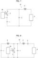
- the configuration of a resonant power conversion device according to a present embodiment will be described with reference to FIG. 1 .
- the resonant power conversion device according to the present embodiment includes: a main circuit 10 that converts and outputs input power; and a drive circuit 20 that drives the main circuit 10.
- a power supply 1 and a load 2 are connected to the main circuit 10.
- the power supply 1 is, for example, a DC power supply.
- the main circuit 10 includes a capacitor 3, an inductor 4, and a semiconductor switch 5.
- the main circuit 10 is a voltage resonant circuit in which the voltage resonates in the period when the semiconductor switch 5 is in the off-state.
- the capacitor 3 and the inductor 4 are connected in series between the power supply 1 and the load 2 in the order from the capacitor 3 to the inductor 4.
- the semiconductor switch 5 is a switching element having a high-potential terminal, a low-potential terminal and a control terminal.
- the semiconductor switch 5 is, for example, a MOSFET, and a drain terminal D, a source terminal S, and a gate terminal G correspond to the high-potential terminal, the low-potential terminal, and the control terminal, respectively.
- the drain terminal D of the semiconductor switch 5 is connected to the connection point between the capacitor 3 and the inductor 4.
- the source terminal S of the semiconductor switch 5 is connected to the power supply 1.
- the drive circuit 20 outputs a control signal to the gate terminal G to drive the semiconductor switch 5.
- the semiconductor switch 5 enters an on-state or an off-state depending on the signal value of a control signal input to the gate terminal G, more specifically, depending on a voltage applied to the gate terminal G (hereinafter referred to as a "control voltage").
- the semiconductor switch 5 When the control voltage exceeds a threshold, the semiconductor switch 5 enters an on-state, that is, the semiconductor switch 5 is switched to ON between the drain terminal D and the source terminal S. When the control voltage is below the threshold, the semiconductor switch 5 enters an off-state, that is, is switched to OFF between the drain terminal D and the source terminal S.
- the control voltage at which the semiconductor switch 5 enters an on-state is called an "on-control voltage”
- the control voltage at which the semiconductor switch 5 enters an off-state is called an "off-control voltage”.
- the drive circuit 20 has two or more types of off-control voltages, that is, two or more types of control voltages at which each voltage is below a threshold.
- the drive circuit 20 can change an off-control voltage using two or more types of off-control voltages. As described later, each of the two or more types of off-control voltages is set in accordance with the resonant frequency to be generated in the main circuit 10.
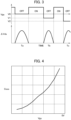
- FIG. 2 and FIG. 3 illustrate the amount of voltage change in the drain-source voltage ⁇ Vds with respect to the control voltage Vgs that is applied to the gate terminal G.
- FIG. 4 illustrates the change of the output capacitance Coss in the semiconductor switch 5 with respect to the control voltage Vgs.
- the drive circuit 20 alternately switches the semiconductor switch 5 between an on-state and an off-state.
- the main circuit 10 which is a voltage resonant circuit
- the drain-source voltage ⁇ Vds vibrates when the semiconductor switch 5 is in the off-state, and a resonant waveform is generated in the amount of voltage change in the drain-source voltage ⁇ Vds.
- the resonant waveform is generated by the capacitor 3, the inductor 4, and the output capacitance Coss in the semiconductor switch 5, and the period thereof relates to the resonant frequency of the main circuit 10 which depends on the capacitor 3, the inductor 4, and the output capacitance Coss in the semiconductor switch 5.
- the resonant frequency is also constant, and thus the amount of voltage change in the drain-source voltage ⁇ Vds is also a resonant waveform with a constant period Ta.
- the drive circuit 20 applies an on-control voltage or an off-control voltage to the gate terminal G at a switching frequency that is based on the resonant frequency of the main circuit 10, which enables soft switching or low-loss switching to be performed.
- FIG. 2 illustrates a half-wave resonance; however, a full-wave resonance is also acceptable.
- the drive circuit 20 is assumed to have three types of off-control voltages, and FIG. 3 illustrates three types of off-control voltages V0, V1, and V2.
- the off-control voltages V0, V1, and V2 are voltage values below the threshold of the semiconductor switch 5, and V1 has a lower voltage than V0, and V2 has a lower voltage than V1.
- the off-control voltage V0 is applied to the first off-period illustrated in FIG. 3
- the off-control voltage V1 is applied to the second off-period coming after the on-period, after the first off-period.
- the off-control voltage V2 is applied to the third off-period coming after the on-period, after the second off-period.
- the output capacitance Coss decreases as the control voltage Vgs decreases. Accordingly, the output capacitance Coss decreases by lowering the off-control voltage that is applied from the drive circuit 20 to the gate terminal G.
- the periods Ta, Tb, and Tc of the resonance waveform become shorter by lowering the off-control voltages V0, V1, and V2. That is, the resonance frequency generated in the main circuit 10 becomes greater.
- the off-control voltages V0, V1, and V2 of the drive circuit 20 are set based on the resonance frequency to be generated in the main circuit 10.
- the drive circuit 20 has two or more types of off-control voltages.
- the output capacitance Coss of the semiconductor switch 5 differs depending on a voltage value of the off-control voltage (type of off-control voltage). Accordingly, the output capacitance Coss of the semiconductor switch 5 behaves like a variable capacitance according to the type of off-control voltage output by the drive circuit 20.
- the resonant frequency generated in the main circuit 10 can be freely controlled. Switching loss can be reduced by harmonizing the resonant frequency generated in the main circuit 10 with the switching frequency.
- it is not necessary to add a circuit component to the main circuit 10 because only two or more types of off-control voltages need to be utilized. This makes it possible to reduce switching loss with a simple circuit configuration.
- each of two or more types of off-control voltages in the drive circuit 20 is set in accordance with the resonance frequency to be generated in the main circuit 10.
- This configuration makes it possible to optionally control the resonance frequency generated in the main circuit 10 according to two or more types of off-control voltages.
- the number of situations in which soft switching can be performed increases by harmonizing the resonance frequency generated in the main circuit 10 with the switching frequency, and thus switching loss can be reduced.
- the drive circuit 20 can change the off-control voltage using two or more types of off-control voltages. According to this configuration, when the drive circuit 20 changes the off-control voltage, the output capacitance Coss of the semiconductor switch 5 behaves like a variable capacitance, and thus the resonant frequency generated in the main circuit 10 can be controlled. The number of situations in which soft switching can be performed increases by harmonizing the resonance frequency generated in the main circuit 10 with the switching frequency, and thus switching loss can be reduced.
- the drive circuit 20 can change the off-control voltage in the preceding off-period to the off-control voltage in the next off-period.
- This configuration makes it possible to change the off-control voltage applied to the gate terminal G for each off-period, and thus it is possible to increase the number of times that the resonant frequency is optimized. For this reason, switching loss can be reduced.
- the drive circuit 20 can change the off-control voltage in the next off-period on the basis of the output of the main circuit 10. It is possible to harmonize the resonant frequency generated in the main circuit 10 with the switching frequency corresponding to the output of the main circuit 10. This increases the number of situations in which soft switching can be performed, and thus switching loss can be reduced.
- the drive circuit 20 makes the off-control voltage in the next coming off-period greater than the off-control voltage in the preceding off-period.
- the drive circuit 20 may change the off-control voltage on the basis of the input of the main circuit 10.
- the resonance frequency of the main circuit 10 changes according to changes in the voltage, current, and temperature of the semiconductor switch 5, the capacitor 3, and the inductor 4. Accordingly, the drive circuit 20 may change the off-control voltage on the basis of the voltage, current, and temperature of the semiconductor switch 5, the capacitor 3, and the inductor 4.
- switching loss can be reduced regardless of input-output fluctuations or environmental fluctuations of the main circuit 10.
- a resonant power conversion device according to a second embodiment will be described below.
- the resonant power conversion device according to the second embodiment differs in the control method of an off-control voltage from the resonant power conversion device according to the first embodiment. Descriptions that are the same as those of the first embodiment are omitted, and differences therefrom will be mainly described below.
- the drive circuit 20 of the first embodiment described above controls an off-control voltage to be kept constant regardless of the transition of time as long as the off-control voltage is within one off-period.
- the drive circuit 20 of the first embodiment switches between two types of off-control voltages V0 and V1 within one off-period. Specifically, the drive circuit 20 outputs an off-control voltage V1 in the first period from timing T0 when the off-period begins until timing T1, and outputs an off-control voltage V0 in the second period from timing T1 until timing T2 when the off-period ends.
- the resonant waveform of the drain-source voltage ⁇ Vds illustrates a response corresponding to the off-control voltage V1 in the first period from timing T0 to timing T1, and a response corresponding to the off-control voltage V0 in the second period from timing T1 to timing T2. Since a resonant waveform with a short period occurs in the first period corresponding to the off-control voltage V1, the period of the resonant waveform is shorter than when the off-control voltage V0 is uniformly applied throughout the off-period.
- the period of the resonance waveform differs by changing the ratio between the first period and the second period. Specifically, when a ratio of the first period increases, the period of the resonance waveform becomes relatively shorter. This makes it possible to increase the resonance frequency generated in the main circuit 10.
- the off-control voltage to be applied in the first period is not limited to the off-control voltage V1, and may be a voltage value as long as it is lower than the off-control voltage V0.
- the period of the resonant waveform becomes relatively shorter as the off-control voltage to be applied in the first period is lower than the off-control voltage to be applied in the second period. This makes it possible to increase the resonance frequency generated in the main circuit 10.
- the drive circuit 20 can change an off-control voltage within one off-period, and thus the resonant frequency generated in the main circuit 10 can be optionally controlled.
- the resonant frequency generated in the main circuit 10 can be harmonize with the switching frequency.
- the number of situations in which soft switching can be performed increases, and thus switching loss can be reduced.
- the drive circuit 20 can change the ratio between the first period and the second period, or change the voltage ratio between the off-control voltage applied in the first period and the offcontrol voltage applied in the second period.
- the resonant frequency generated in the main circuit 10 can be flexibly controlled.
- the drive circuit 20 can change the ratio between the first period and second period or the voltage ratio therebetween, based on the input and output of the main circuit 10 and based on one or more values among the voltage, current, and temperature of the semiconductor switch 5, the capacitor 3, and the inductor 4.
- switching loss can be reduced regardless of input and output fluctuations or environmental fluctuations of the main circuit 10.
- the drive circuit 20 performs switching in one off-period using two types of off-control voltages. However, the drive circuit 20 may perform switching using three or more types of off-control voltages.
- the drive circuit 20 switches from a low off-control voltage to a high offcontrol voltage when switching from the first period to the second period.
- the voltage at the end of the off-period becomes a high off-control voltage. For this reason, since the deviation from an on-control voltage is small, the transition to an on-period can be performed smoothly.
- the drive circuit 20 may switch from a high off-control voltage to a low off-control voltage when switching from the first period to the second period.
- the drive circuit 20 changes an off-control voltage in a stepwise manner.
- the drive circuit 20 may continuously change an off-control voltage in accordance with the transition of time within one off-period.
- the offcontrol voltage becomes V1 at the beginning of the off-period, continuously rises in accordance with the transition of time, and becomes V0 at the beginning of the off-period.
- the period of the resonant waveform becomes relatively shorter than when the off-control voltage V0 is uniformly applied throughout the off-period. This makes it possible to appropriately control the resonant frequency generated in the main circuit 10. Note that the example illustrated in FIG. 6 is not covered by the subject-matter of the claims.
- the drive circuit 20 can change the slope of an off-control voltage by changing one or both of an off-control voltage at the beginning of the off-period and an off-control voltage at the end of the off-period. This makes it possible to appropriately control the resonant frequency generated in the main circuit 10.
- the drive circuit 20 changes an off-control voltage linearly from the beginning to the end of the off-period, but the drive circuit 20 is limited thereto.
- the drive circuit 20 may change an off-control voltage non-linearly.
- FIG. 1 illustrates the configuration of the main circuit 10.
- the main circuit 10 is not limited to a voltage resonant circuit, and may be a current resonant circuit in which the current resonates in the period when the semiconductor switch 5 is in the on-state.
- the main circuit 10 may form a resonant circuit by connecting the capacitor 3 in parallel to the power supply 1.
- the main circuit 10 further includes a capacitor 7 and an inductor 8, and functions as a class-E amplifier circuit.
- the inductor 8 has a function of keeping the current constant, and the capacitor 7 is provided such that the current flows to the load 2 in the time domain in which the semiconductor switch 5 enters an off-state.
- a MOSFET is illustrated as an example of the semiconductor switch 5.
- a switching element of the main circuit 10 other than a unipolar type, a bipolar type, or a bandgap of an element material may be used.
- a semiconductor switch may enter an off-state or an on-state depending on the signal value of a control signal input to a control terminal, more specifically, the current supplied to a control terminal (hereinafter referred to as a "control current"). Accordingly, a semiconductor switch enters an on-state when the control current exceeds a threshold. In contrast, a semiconductor switch enters an off-state when the control current is below a threshold.
- the control voltage at which the semiconductor switch 5 enters an on-state is called an "on-control voltage”
- the control voltage at which the semiconductor switch 5 enters an off-state is called an "off-control voltage”.
- the drive circuit 20 has two or more types of off-control currents, that is, two or more types of control currents at which each current is below a threshold.
- the drive circuit 20 can optionally change two or more types of off-control currents, and each of two or more types of off-control voltages is set based on the resonant frequency to be generated in the main circuit 10, as in the above-described embodiment.
Landscapes
- Engineering & Computer Science (AREA)
- Power Engineering (AREA)
- Dc-Dc Converters (AREA)
- Power Conversion In General (AREA)
- Inverter Devices (AREA)
Claims (6)
- Eine resonante Energieumwandlungsvorrichtung, aufweisend:eine Hauptschaltung (10), die mit einem Halbleiterschaltelement (5) mit einem Hochpotentialanschluss (D), einem Niedrigpotentialanschluss (S) und einem Steueranschluss (G) bereitgestellt wird, und mit einem Kondensator (3) und einem Induktor (4) bereitgestellt wird, die in Reihe oder parallel mit dem Hochpotentialanschluss (D) oder dem Niedrigpotentialanschluss (S) geschaltet sind, und wobei die Hauptschaltung (10) konfiguriert ist, um Eingangsleistung umzuwandeln und auszugeben; undeine Treiberschaltung (20), die konfiguriert ist, um ein Steuersignal (Vgs) an den Steueranschluss (G) auszugeben und das Halbleiterschaltelement (5) mit einer erforderlichen Schaltfrequenz anzusteuern,wobei das Halbleiterschaltelement (5) konfiguriert ist, um in Abhängigkeit von einem Signalwert des an den Steueranschluss (G) eingegebenen Steuersignals (Vgs) in einen Aus-Zustand oder einen Ein-Zustand zu wechseln,dadurch gekennzeichnet, dass:sich die Ausgabekapazität des Halbleiterschaltelements (5) in seinem Aus-Zustand entsprechend dem Signalwert des Steuersignals (Vgs) wie eine variable Kapazität verhält,die Treiberschaltung (20) konfiguriert ist, um die Resonanzfrequenz in der Hauptschaltung durch Änderung des Signalwerts des Steuersignals (Vgs), bei dem das Halbleiterschaltelement (5) in den Aus-Zustand wechselt, unter Verwendung von zwei oder mehr Steuersignalwerten (V0, V1, V2) für den Aus-Zustand zu steuern,wobei die Treiberschaltung (20) konfiguriert ist, um beim Wechsel des Halbleiterschaltelements (5) zu einer zweiten Aus-Periode, die nach einer Ein-Periode nach einer ersten Aus-Periode kommt, einen Signalwert des Steuersignals (V gs) in der zweiten Aus-Periode von einem Signalwert des Steuersignals (Vgs) in der ersten Aus-Periode ändert, um die in der Hauptschaltung erzeugte Resonanzfrequenz mit der Schaltfrequenz in Einklang zu bringen, um so den Schaltverlust zu reduzieren.
- Die resonante Energieumwandlungsvorrichtung gemäß Anspruch 1, wobei
die Treiberschaltung (20) konfiguriert ist, um den Signalwert des Steuersignals (Vgs) in der zweiten Aus-Periode von dem Signalwert des Steuersignals in der ersten Aus-Periode zu ändern, basierend auf einem Eingang und einem Ausgang der Hauptschaltung (10) und basierend auf einem oder mehreren Werten von Spannung, Strom und Temperatur des Halbleiterschalters, des Kondensators (3) und des Induktors (4). - Die resonante Energieumwandlungsvorrichtung gemäß Anspruch 2, wobei
die Treiberschaltung (20) konfiguriert ist, um bei einem Anstieg des Ausgangs der Hauptschaltung (10) den Signalwert des Steuersignals (Vgs) in der zweiten Aus-Periode größer als den Signalwert des Steuersignals in der ersten Aus-Periode zu machen. - Eine resonante Energieumwandlungsvorrichtung, aufweisend:eine Hauptschaltung (10), die mit einem Halbleiterschaltelement (5) mit einem Hochpotentialanschluss (D), einem Niedrigpotentialanschluss (S) und einem Steueranschluss (G) bereitgestellt wird, und mit einem Kondensator (3) und einem Induktor (4) bereitgestellt wird, die in Reihe oder parallel mit dem Hochpotentialanschluss (D) oder dem Niedrigpotentialanschluss (S) geschaltet sind, und wobei die Hauptschaltung (10) konfiguriert ist, um Eingangsleistung umzuwandeln und auszugeben; undeine Treiberschaltung (20), die konfiguriert ist, um ein Steuersignal (Vgs) an den Steueranschluss (G) auszugeben und das Halbleiterschaltelement (5) mit einer erforderlichen Schaltfrequenz anzusteuern,wobei das Halbleiterschaltelement (5) konfiguriert ist, um in Abhängigkeit von einem Signalwert des an den Steueranschluss (G) eingegebenen Steuersignals (Vgs) in einen Aus-Zustand oder einen Ein-Zustand zu wechseln,dadurch gekennzeichnet, dass:sich die Ausgabekapazität des Halbleiterschaltelements (5) in seinem Aus-Zustand entsprechend dem Signalwert des Steuersignals (Vgs) wie eine variable Kapazität verhält,die Treiberschaltung (20) konfiguriert ist, um die Resonanzfrequenz in der Hauptschaltung durch Änderung des Signalwerts des Steuersignals (Vgs) in einer Aus-Periode ein- oder mehrmals zu steuern, wobei die Treiberschaltung (20) konfiguriert ist, um in der Aus-Periode eine erste Periode, in der der Signalwert (V1) des Steuersignals niedrig ist, und eine zweiten Periode, in der der Signalwert (V0) des Steuersignals größer ist als der der ersten Periode, einzustellen, wobei die Signalwerte (V1, V0) des Steuersignals in der ersten Periode und in der zweiten Periode so eingestellt werden, dass eine in der Hauptschaltung (10) zu erzeugende Resonanzfrequenz mit der erforderlichen Schaltfrequenz harmoniert, um so den Schaltverlust zu reduzieren.
- Die resonante Energieumwandlungsvorrichtung gemäß Anspruch 4, wobei
die Treiberschaltung (20) konfiguriert ist, um ein oder beide Verhältnisse zwischen der ersten Periode und der zweiten Periode in der Aus-Periode und einem Verhältnis des Signalwerts des Steuersignals (Vgs) in der ersten Periode und des Signalwerts des Steuersignals in der zweiten Periode zu ändern, basierend auf einem Eingang und Ausgang der Hauptschaltung (10) und basierend auf einem oder mehreren Werten von Spannung, Strom und Temperatur des Halbleiterschaltelements (5), des Kondensators (3) und des Induktors (4). - Die resonante Energieumwandlungsvorrichtung gemäß Anspruch 4 oder 5, wobei
die Treiberschaltung (20) konfiguriert ist, um die erste Periode und die zweite Periode in der Aus-Periode, in der Reihenfolge von der ersten Periode zur zweiten Periode, einzustellen.
Applications Claiming Priority (1)
| Application Number | Priority Date | Filing Date | Title |
|---|---|---|---|
| PCT/IB2020/000926 WO2022096907A1 (ja) | 2020-11-06 | 2020-11-06 | 共振型電力変換装置 |
Publications (3)
| Publication Number | Publication Date |
|---|---|
| EP4243260A1 EP4243260A1 (de) | 2023-09-13 |
| EP4243260A4 EP4243260A4 (de) | 2024-01-10 |
| EP4243260B1 true EP4243260B1 (de) | 2024-12-18 |
Family
ID=81457565
Family Applications (1)
| Application Number | Title | Priority Date | Filing Date |
|---|---|---|---|
| EP20960735.7A Active EP4243260B1 (de) | 2020-11-06 | 2020-11-06 | Resonanzleistungsumwandlungsvorrichtung |
Country Status (6)
| Country | Link |
|---|---|
| US (1) | US11916469B2 (de) |
| EP (1) | EP4243260B1 (de) |
| JP (1) | JP7514949B2 (de) |
| CN (1) | CN116491056B (de) |
| MX (1) | MX2023005164A (de) |
| WO (1) | WO2022096907A1 (de) |
Family Cites Families (18)
| Publication number | Priority date | Publication date | Assignee | Title |
|---|---|---|---|---|
| US4720668A (en) * | 1986-06-20 | 1988-01-19 | Lee Fred C | Zero-voltage switching quasi-resonant converters |
| JPH06243985A (ja) | 1993-02-15 | 1994-09-02 | Matsushita Electric Works Ltd | 放電灯点灯装置 |
| JP3237633B2 (ja) * | 1998-12-02 | 2001-12-10 | 株式会社村田製作所 | スイッチング電源装置 |
| JP2001286134A (ja) | 2000-04-03 | 2001-10-12 | Nagano Japan Radio Co | スイッチング電源装置 |
| JP2003111394A (ja) * | 2001-09-28 | 2003-04-11 | Matsushita Electric Ind Co Ltd | Dc−dcコンバータ |
| KR100791717B1 (ko) * | 2004-12-08 | 2008-01-03 | 산켄덴키 가부시키가이샤 | 다출력 전류 공진형 dc-dc 컨버터 |
| JP2007236010A (ja) * | 2006-02-02 | 2007-09-13 | Sony Corp | スイッチング電源回路 |
| JP2009017749A (ja) | 2007-07-09 | 2009-01-22 | Fujitsu Ten Ltd | 電源回路、電源制御装置、及び、電源装置 |
| JP2009254062A (ja) | 2008-04-03 | 2009-10-29 | Tokyo Metropolitan Univ | 共振型dcチョッパ回路 |
| GB2468490A (en) * | 2009-03-09 | 2010-09-15 | Koen Geirnaert | Resonant power converter having variable output power or switching frequency |
| JP5197658B2 (ja) * | 2010-03-10 | 2013-05-15 | 株式会社東芝 | 駆動回路 |
| JP6090007B2 (ja) | 2013-06-26 | 2017-03-08 | 株式会社デンソー | 駆動回路 |
| JP5930560B1 (ja) * | 2015-01-30 | 2016-06-08 | 株式会社京三製作所 | 高周波絶縁ゲートドライバ回路、及びゲート回路駆動方法 |
| JP6565485B2 (ja) | 2015-08-25 | 2019-08-28 | 船井電機株式会社 | 給電装置 |
| JP6610679B2 (ja) * | 2015-12-04 | 2019-11-27 | 株式会社村田製作所 | 電力変換装置 |
| JP2018056737A (ja) | 2016-09-28 | 2018-04-05 | パナソニックIpマネジメント株式会社 | 半導体スイッチング素子の駆動回路 |
| JP2018074676A (ja) * | 2016-10-26 | 2018-05-10 | 株式会社デンソー | ゲート駆動回路 |
| JP6930266B2 (ja) * | 2017-07-24 | 2021-09-01 | 富士電機株式会社 | 電力変換装置の駆動方法 |
-
2020
- 2020-11-06 EP EP20960735.7A patent/EP4243260B1/de active Active
- 2020-11-06 WO PCT/IB2020/000926 patent/WO2022096907A1/ja not_active Ceased
- 2020-11-06 MX MX2023005164A patent/MX2023005164A/es unknown
- 2020-11-06 CN CN202080106791.XA patent/CN116491056B/zh active Active
- 2020-11-06 JP JP2022560419A patent/JP7514949B2/ja active Active
- 2020-11-06 US US18/251,307 patent/US11916469B2/en active Active
Also Published As
| Publication number | Publication date |
|---|---|
| US11916469B2 (en) | 2024-02-27 |
| JP7514949B2 (ja) | 2024-07-11 |
| CN116491056A (zh) | 2023-07-25 |
| MX2023005164A (es) | 2023-11-08 |
| WO2022096907A1 (ja) | 2022-05-12 |
| EP4243260A4 (de) | 2024-01-10 |
| CN116491056B (zh) | 2024-06-21 |
| JPWO2022096907A1 (de) | 2022-05-12 |
| US20230412062A1 (en) | 2023-12-21 |
| EP4243260A1 (de) | 2023-09-13 |
Similar Documents
| Publication | Publication Date | Title |
|---|---|---|
| US6222351B1 (en) | Dual supply device with a single direct-current/direct-current converter and capacitive translator | |
| US6262564B1 (en) | Driver for a controllable switch in a power converter | |
| US11245324B2 (en) | Switching converter and a method thereof | |
| EP0992103B1 (de) | Kombinierter kapazitiver aufwärts/abwärtswandler | |
| TWI424673B (zh) | 用於同步昇壓轉換器之同步整流器控制系統及方法 | |
| KR102802538B1 (ko) | 게이트 드라이버를 위한 부트스트랩 회로 | |
| US8148957B2 (en) | Power switch-mode circuit with devices of different threshold voltages | |
| US11196413B2 (en) | Driving circuit for switching element, and switching circuit | |
| KR101820232B1 (ko) | 전력 변환기 회로를 동작시키기 위한 방법 및 전력 변환기 회로 | |
| US6472852B1 (en) | Resonant buck-type voltage converter using swinging inductance | |
| KR101935452B1 (ko) | Dc-dc 컨버터 및 이를 포함하는 2단 전력단 컨버터 | |
| CN114825918B (zh) | Cot控制电路、方法以及相关集成电路 | |
| US20150249387A1 (en) | Power-supply apparatus | |
| KR102572644B1 (ko) | 동기buck회로의 제어 방법, 장치, 시스템 및 전자장치 | |
| CN119602599A (zh) | 用于降压转换器中相节点的转换速率控制的驱动器 | |
| CN107634649B (zh) | 一种开关器件驱动电路、方法及电压转换电路 | |
| Qu et al. | A fully soft switched point-of-load converter for resource constraint drone applications | |
| US20250266746A1 (en) | Two-Phase Smart Power Stage (SPS) for Multiphase Buck Converters | |
| US20120307536A1 (en) | Synchronous rectifier driver circuit rectifier | |
| EP4436043A1 (de) | Signalerfassung von kaskodenleistungsvorrichtungen | |
| US11916469B2 (en) | Resonant power conversion device | |
| Zhang et al. | Design optimization for a GaN FET-based three-level synchronous buck converter | |
| Górecki et al. | Thermal limits of the maximum operating frequency of SiC MOSFETs | |
| US12355441B2 (en) | Level-shifter and its use with switching converters | |
| Parashar et al. | A gate driver for synchronous buck converter with normally on semiconductor switches |
Legal Events
| Date | Code | Title | Description |
|---|---|---|---|
| STAA | Information on the status of an ep patent application or granted ep patent |
Free format text: STATUS: THE INTERNATIONAL PUBLICATION HAS BEEN MADE |
|
| PUAI | Public reference made under article 153(3) epc to a published international application that has entered the european phase |
Free format text: ORIGINAL CODE: 0009012 |
|
| STAA | Information on the status of an ep patent application or granted ep patent |
Free format text: STATUS: REQUEST FOR EXAMINATION WAS MADE |
|
| 17P | Request for examination filed |
Effective date: 20230606 |
|
| AK | Designated contracting states |
Kind code of ref document: A1 Designated state(s): AL AT BE BG CH CY CZ DE DK EE ES FI FR GB GR HR HU IE IS IT LI LT LU LV MC MK MT NL NO PL PT RO RS SE SI SK SM TR |
|
| REG | Reference to a national code |
Ref country code: DE Ref legal event code: R079 Free format text: PREVIOUS MAIN CLASS: H02M0001080000 Ipc: H02M0007480000 Ref document number: 602020043554 Country of ref document: DE |
|
| A4 | Supplementary search report drawn up and despatched |
Effective date: 20231208 |
|
| RIC1 | Information provided on ipc code assigned before grant |
Ipc: H02M 1/08 20060101ALI20231204BHEP Ipc: H02M 7/48 20070101AFI20231204BHEP |
|
| DAV | Request for validation of the european patent (deleted) | ||
| DAX | Request for extension of the european patent (deleted) | ||
| GRAP | Despatch of communication of intention to grant a patent |
Free format text: ORIGINAL CODE: EPIDOSNIGR1 |
|
| STAA | Information on the status of an ep patent application or granted ep patent |
Free format text: STATUS: GRANT OF PATENT IS INTENDED |
|
| INTG | Intention to grant announced |
Effective date: 20240923 |
|
| GRAS | Grant fee paid |
Free format text: ORIGINAL CODE: EPIDOSNIGR3 |
|
| GRAA | (expected) grant |
Free format text: ORIGINAL CODE: 0009210 |
|
| STAA | Information on the status of an ep patent application or granted ep patent |
Free format text: STATUS: THE PATENT HAS BEEN GRANTED |
|
| AK | Designated contracting states |
Kind code of ref document: B1 Designated state(s): AL AT BE BG CH CY CZ DE DK EE ES FI FR GB GR HR HU IE IS IT LI LT LU LV MC MK MT NL NO PL PT RO RS SE SI SK SM TR |
|
| REG | Reference to a national code |
Ref country code: CH Ref legal event code: EP |
|
| REG | Reference to a national code |
Ref country code: DE Ref legal event code: R096 Ref document number: 602020043554 Country of ref document: DE |
|
| REG | Reference to a national code |
Ref country code: IE Ref legal event code: FG4D |
|
| REG | Reference to a national code |
Ref country code: LT Ref legal event code: MG9D |
|
| PG25 | Lapsed in a contracting state [announced via postgrant information from national office to epo] |
Ref country code: HR Free format text: LAPSE BECAUSE OF FAILURE TO SUBMIT A TRANSLATION OF THE DESCRIPTION OR TO PAY THE FEE WITHIN THE PRESCRIBED TIME-LIMIT Effective date: 20241218 |
|
| PG25 | Lapsed in a contracting state [announced via postgrant information from national office to epo] |
Ref country code: FI Free format text: LAPSE BECAUSE OF FAILURE TO SUBMIT A TRANSLATION OF THE DESCRIPTION OR TO PAY THE FEE WITHIN THE PRESCRIBED TIME-LIMIT Effective date: 20241218 |
|
| PG25 | Lapsed in a contracting state [announced via postgrant information from national office to epo] |
Ref country code: BG Free format text: LAPSE BECAUSE OF FAILURE TO SUBMIT A TRANSLATION OF THE DESCRIPTION OR TO PAY THE FEE WITHIN THE PRESCRIBED TIME-LIMIT Effective date: 20241218 |
|
| PG25 | Lapsed in a contracting state [announced via postgrant information from national office to epo] |
Ref country code: NO Free format text: LAPSE BECAUSE OF FAILURE TO SUBMIT A TRANSLATION OF THE DESCRIPTION OR TO PAY THE FEE WITHIN THE PRESCRIBED TIME-LIMIT Effective date: 20250318 |
|
| REG | Reference to a national code |
Ref country code: NL Ref legal event code: MP Effective date: 20241218 |
|
| PG25 | Lapsed in a contracting state [announced via postgrant information from national office to epo] |
Ref country code: GR Free format text: LAPSE BECAUSE OF FAILURE TO SUBMIT A TRANSLATION OF THE DESCRIPTION OR TO PAY THE FEE WITHIN THE PRESCRIBED TIME-LIMIT Effective date: 20250319 Ref country code: LV Free format text: LAPSE BECAUSE OF FAILURE TO SUBMIT A TRANSLATION OF THE DESCRIPTION OR TO PAY THE FEE WITHIN THE PRESCRIBED TIME-LIMIT Effective date: 20241218 |
|
| PG25 | Lapsed in a contracting state [announced via postgrant information from national office to epo] |
Ref country code: RS Free format text: LAPSE BECAUSE OF FAILURE TO SUBMIT A TRANSLATION OF THE DESCRIPTION OR TO PAY THE FEE WITHIN THE PRESCRIBED TIME-LIMIT Effective date: 20250318 |
|
| PG25 | Lapsed in a contracting state [announced via postgrant information from national office to epo] |
Ref country code: NL Free format text: LAPSE BECAUSE OF FAILURE TO SUBMIT A TRANSLATION OF THE DESCRIPTION OR TO PAY THE FEE WITHIN THE PRESCRIBED TIME-LIMIT Effective date: 20241218 |
|
| REG | Reference to a national code |
Ref country code: AT Ref legal event code: MK05 Ref document number: 1753052 Country of ref document: AT Kind code of ref document: T Effective date: 20241218 |
|
| PG25 | Lapsed in a contracting state [announced via postgrant information from national office to epo] |
Ref country code: SM Free format text: LAPSE BECAUSE OF FAILURE TO SUBMIT A TRANSLATION OF THE DESCRIPTION OR TO PAY THE FEE WITHIN THE PRESCRIBED TIME-LIMIT Effective date: 20241218 |
|
| PG25 | Lapsed in a contracting state [announced via postgrant information from national office to epo] |
Ref country code: PL Free format text: LAPSE BECAUSE OF FAILURE TO SUBMIT A TRANSLATION OF THE DESCRIPTION OR TO PAY THE FEE WITHIN THE PRESCRIBED TIME-LIMIT Effective date: 20241218 |
|
| PG25 | Lapsed in a contracting state [announced via postgrant information from national office to epo] |
Ref country code: ES Free format text: LAPSE BECAUSE OF FAILURE TO SUBMIT A TRANSLATION OF THE DESCRIPTION OR TO PAY THE FEE WITHIN THE PRESCRIBED TIME-LIMIT Effective date: 20241218 |
|
| PG25 | Lapsed in a contracting state [announced via postgrant information from national office to epo] |
Ref country code: IS Free format text: LAPSE BECAUSE OF FAILURE TO SUBMIT A TRANSLATION OF THE DESCRIPTION OR TO PAY THE FEE WITHIN THE PRESCRIBED TIME-LIMIT Effective date: 20250418 |
|
| PG25 | Lapsed in a contracting state [announced via postgrant information from national office to epo] |
Ref country code: PT Free format text: LAPSE BECAUSE OF FAILURE TO SUBMIT A TRANSLATION OF THE DESCRIPTION OR TO PAY THE FEE WITHIN THE PRESCRIBED TIME-LIMIT Effective date: 20250421 |
|
| PG25 | Lapsed in a contracting state [announced via postgrant information from national office to epo] |
Ref country code: EE Free format text: LAPSE BECAUSE OF FAILURE TO SUBMIT A TRANSLATION OF THE DESCRIPTION OR TO PAY THE FEE WITHIN THE PRESCRIBED TIME-LIMIT Effective date: 20241218 |
|
| PG25 | Lapsed in a contracting state [announced via postgrant information from national office to epo] |
Ref country code: AT Free format text: LAPSE BECAUSE OF FAILURE TO SUBMIT A TRANSLATION OF THE DESCRIPTION OR TO PAY THE FEE WITHIN THE PRESCRIBED TIME-LIMIT Effective date: 20241218 Ref country code: RO Free format text: LAPSE BECAUSE OF FAILURE TO SUBMIT A TRANSLATION OF THE DESCRIPTION OR TO PAY THE FEE WITHIN THE PRESCRIBED TIME-LIMIT Effective date: 20241218 |
|
| PG25 | Lapsed in a contracting state [announced via postgrant information from national office to epo] |
Ref country code: SK Free format text: LAPSE BECAUSE OF FAILURE TO SUBMIT A TRANSLATION OF THE DESCRIPTION OR TO PAY THE FEE WITHIN THE PRESCRIBED TIME-LIMIT Effective date: 20241218 |
|
| PG25 | Lapsed in a contracting state [announced via postgrant information from national office to epo] |
Ref country code: CZ Free format text: LAPSE BECAUSE OF FAILURE TO SUBMIT A TRANSLATION OF THE DESCRIPTION OR TO PAY THE FEE WITHIN THE PRESCRIBED TIME-LIMIT Effective date: 20241218 |
|
| PG25 | Lapsed in a contracting state [announced via postgrant information from national office to epo] |
Ref country code: IT Free format text: LAPSE BECAUSE OF FAILURE TO SUBMIT A TRANSLATION OF THE DESCRIPTION OR TO PAY THE FEE WITHIN THE PRESCRIBED TIME-LIMIT Effective date: 20241218 |
|
| PG25 | Lapsed in a contracting state [announced via postgrant information from national office to epo] |
Ref country code: SE Free format text: LAPSE BECAUSE OF FAILURE TO SUBMIT A TRANSLATION OF THE DESCRIPTION OR TO PAY THE FEE WITHIN THE PRESCRIBED TIME-LIMIT Effective date: 20241218 |
|
| REG | Reference to a national code |
Ref country code: DE Ref legal event code: R097 Ref document number: 602020043554 Country of ref document: DE |
|
| PG25 | Lapsed in a contracting state [announced via postgrant information from national office to epo] |
Ref country code: DK Free format text: LAPSE BECAUSE OF FAILURE TO SUBMIT A TRANSLATION OF THE DESCRIPTION OR TO PAY THE FEE WITHIN THE PRESCRIBED TIME-LIMIT Effective date: 20241218 |
|
| PLBE | No opposition filed within time limit |
Free format text: ORIGINAL CODE: 0009261 |
|
| STAA | Information on the status of an ep patent application or granted ep patent |
Free format text: STATUS: NO OPPOSITION FILED WITHIN TIME LIMIT |
|
| REG | Reference to a national code |
Ref country code: CH Ref legal event code: L10 Free format text: ST27 STATUS EVENT CODE: U-0-0-L10-L00 (AS PROVIDED BY THE NATIONAL OFFICE) Effective date: 20251029 |
|
| 26N | No opposition filed |
Effective date: 20250919 |
|
| PGFP | Annual fee paid to national office [announced via postgrant information from national office to epo] |
Ref country code: DE Payment date: 20251022 Year of fee payment: 6 |
|
| PGFP | Annual fee paid to national office [announced via postgrant information from national office to epo] |
Ref country code: GB Payment date: 20251016 Year of fee payment: 6 |
|
| PGFP | Annual fee paid to national office [announced via postgrant information from national office to epo] |
Ref country code: FR Payment date: 20251010 Year of fee payment: 6 |
|
| REG | Reference to a national code |
Ref country code: CH Ref legal event code: H13 Free format text: ST27 STATUS EVENT CODE: U-0-0-H10-H13 (AS PROVIDED BY THE NATIONAL OFFICE) Effective date: 20260623 |
|
| PG25 | Lapsed in a contracting state [announced via postgrant information from national office to epo] |
Ref country code: LT Free format text: LAPSE BECAUSE OF FAILURE TO SUBMIT A TRANSLATION OF THE DESCRIPTION OR TO PAY THE FEE WITHIN THE PRESCRIBED TIME-LIMIT Effective date: 20241218 |
|
| PG25 | Lapsed in a contracting state [announced via postgrant information from national office to epo] |
Ref country code: MC Free format text: LAPSE BECAUSE OF FAILURE TO SUBMIT A TRANSLATION OF THE DESCRIPTION OR TO PAY THE FEE WITHIN THE PRESCRIBED TIME-LIMIT Effective date: 20241218 |
|
| PG25 | Lapsed in a contracting state [announced via postgrant information from national office to epo] |
Ref country code: LU Free format text: LAPSE BECAUSE OF NON-PAYMENT OF DUE FEES Effective date: 20251106 Ref country code: CH Free format text: LAPSE BECAUSE OF NON-PAYMENT OF DUE FEES Effective date: 20251130 |