EP4224512A1 - Substrate bonding method and substrate bonding system - Google Patents
Substrate bonding method and substrate bonding system Download PDFInfo
- Publication number
- EP4224512A1 EP4224512A1 EP21875137.8A EP21875137A EP4224512A1 EP 4224512 A1 EP4224512 A1 EP 4224512A1 EP 21875137 A EP21875137 A EP 21875137A EP 4224512 A1 EP4224512 A1 EP 4224512A1
- Authority
- EP
- European Patent Office
- Prior art keywords
- bonding
- substrates
- substrate
- activation treatment
- gas
- Prior art date
- Legal status (The legal status is an assumption and is not a legal conclusion. Google has not performed a legal analysis and makes no representation as to the accuracy of the status listed.)
- Withdrawn
Links
Images


Classifications
-
- H—ELECTRICITY
- H01—ELECTRIC ELEMENTS
- H01L—SEMICONDUCTOR DEVICES NOT COVERED BY CLASS H10
- H01L21/00—Processes or apparatus adapted for the manufacture or treatment of semiconductor or solid state devices or of parts thereof
- H01L21/02—Manufacture or treatment of semiconductor devices or of parts thereof
-
- B—PERFORMING OPERATIONS; TRANSPORTING
- B32—LAYERED PRODUCTS
- B32B—LAYERED PRODUCTS, i.e. PRODUCTS BUILT-UP OF STRATA OF FLAT OR NON-FLAT, e.g. CELLULAR OR HONEYCOMB, FORM
- B32B37/00—Methods or apparatus for laminating, e.g. by curing or by ultrasonic bonding
- B32B37/12—Methods or apparatus for laminating, e.g. by curing or by ultrasonic bonding characterised by using adhesives
-
- B—PERFORMING OPERATIONS; TRANSPORTING
- B32—LAYERED PRODUCTS
- B32B—LAYERED PRODUCTS, i.e. PRODUCTS BUILT-UP OF STRATA OF FLAT OR NON-FLAT, e.g. CELLULAR OR HONEYCOMB, FORM
- B32B37/00—Methods or apparatus for laminating, e.g. by curing or by ultrasonic bonding
- B32B37/10—Methods or apparatus for laminating, e.g. by curing or by ultrasonic bonding characterised by the pressing technique, e.g. using action of vacuum or fluid pressure
-
- B—PERFORMING OPERATIONS; TRANSPORTING
- B32—LAYERED PRODUCTS
- B32B—LAYERED PRODUCTS, i.e. PRODUCTS BUILT-UP OF STRATA OF FLAT OR NON-FLAT, e.g. CELLULAR OR HONEYCOMB, FORM
- B32B38/00—Ancillary operations in connection with laminating processes
- B32B38/10—Removing layers, or parts of layers, mechanically or chemically
-
- B—PERFORMING OPERATIONS; TRANSPORTING
- B32—LAYERED PRODUCTS
- B32B—LAYERED PRODUCTS, i.e. PRODUCTS BUILT-UP OF STRATA OF FLAT OR NON-FLAT, e.g. CELLULAR OR HONEYCOMB, FORM
- B32B2309/00—Parameters for the laminating or treatment process; Apparatus details
- B32B2309/04—Time
-
- B—PERFORMING OPERATIONS; TRANSPORTING
- B32—LAYERED PRODUCTS
- B32B—LAYERED PRODUCTS, i.e. PRODUCTS BUILT-UP OF STRATA OF FLAT OR NON-FLAT, e.g. CELLULAR OR HONEYCOMB, FORM
- B32B2309/00—Parameters for the laminating or treatment process; Apparatus details
- B32B2309/12—Pressure
-
- B—PERFORMING OPERATIONS; TRANSPORTING
- B32—LAYERED PRODUCTS
- B32B—LAYERED PRODUCTS, i.e. PRODUCTS BUILT-UP OF STRATA OF FLAT OR NON-FLAT, e.g. CELLULAR OR HONEYCOMB, FORM
- B32B2310/00—Treatment by energy or chemical effects
- B32B2310/08—Treatment by energy or chemical effects by wave energy or particle radiation
- B32B2310/0875—Treatment by energy or chemical effects by wave energy or particle radiation using particle radiation
- B32B2310/0881—Treatment by energy or chemical effects by wave energy or particle radiation using particle radiation using ion-radiation, e.g. alpha-rays
-
- B—PERFORMING OPERATIONS; TRANSPORTING
- B32—LAYERED PRODUCTS
- B32B—LAYERED PRODUCTS, i.e. PRODUCTS BUILT-UP OF STRATA OF FLAT OR NON-FLAT, e.g. CELLULAR OR HONEYCOMB, FORM
- B32B2310/00—Treatment by energy or chemical effects
- B32B2310/14—Corona, ionisation, electrical discharge, plasma treatment
Definitions
- the present disclosure relates to a substrate bonding method and a substrate bonding system.
- This substrate bonding method is a method for bonding two substrates to each other by generating hydroxyl groups (OH groups) on the bonding surfaces of the two substrates and causing hydrogen bonds to be formed between the bonding surfaces by bringing the bonding surfaces of the two substrates into contact with each other and applying pressure to the substrates.
- OH groups hydroxyl groups
- the bonding surfaces to be bonded to each other of the two substrates are subjected to reactive ion etching by exposing the bonding surfaces to oxygen plasma, the bonding surfaces of the two substrates are irradiated with nitrogen radicals. Subsequently, by bringing the bonding surfaces of the two substrates into contact with each other and applying pressure to the substrates, the two substrates are bonded to each other.
- Patent Literature 1 Unexamined Japanese Patent Application Publication No. 2005-79353
- the present disclosure has been made in consideration of the above-described conditions, and an objective of the present disclosure is to provide a substrate bonding method and a substrate bonding system that are capable of firmly bonding two substrates to each other.
- a substrate bonding method is a substrate bonding method for bonding two substrates and includes:
- a substrate bonding system is a substrate bonding system for bonding two substrates and includes:
- the bonding surface of the substrate is activated.
- nitrogen plasma or nitrogen radical treatment a state in which nitrogen is adsorbed on the surface or an oxynitride is formed on the surface is formed on the surface of the substrate.
- This state is herein referred to as an N-activated state.
- the N-activated state reacts with water and forms OH groups and thereby contributes to increase in bonding strength.
- the N-activated state formed on the bonding surface of the substrate is unstable and is to be deactivated when left untreated.
- the bonding surfaces are required to be in contact with water molecules within a predetermined standard time after the bonding surfaces of the substrates are activated.
- the bonding surfaces of the substrates are exposed to gas containing water within a predetermined standard time after the bonding surfaces of the substrates are activated. Since, through this processing, it is possible to cause the bonding surfaces of the substrates to come into contact with water molecules while being N-activated, a large number of oxynitrides can be formed on the bonding surfaces of the substrates.
- the substrate bonding system according to present embodiment is a system that, by, after subjecting bonding surfaces of two substrates to activation treatment in a chamber under reduced pressure, bringing the substrates into contact with each other and applying pressure to and heating the substrates, bonds the two substrates to each other.
- the activation treatment by subjecting at least one of the bonding surfaces to be bonded to each other of the respective ones of the two substrates to at least one of reactive ion etching using nitrogen gas and irradiation of nitrogen radicals, the bonding surface of the substrate is activated.
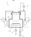
- the substrate bonding system includes feeding ports 811 and 812, a take-out port 813, a first transportation device 82, a cleaning device 3, a turnover device 4, an activation treatment device 2, a substrate bonding device 1, a second transportation device 84, a controller 9, and a load lock chamber 83, as illustrated in FIG. 1 .
- the controller 9 controls the first transportation device 82, the cleaning device 3, the turnover device 4, the activation treatment device 2, the substrate bonding device 1, and the second transportation device 84.
- a high efficiency particulate air (HEPA) filter (not illustrated) is installed. Because of this configuration, the insides of the first transportation device 82, the second transportation device 84, and the cleaning device 3 are maintained at an atmospheric pressure environment that contains an extremely small number of particles.
- HEPA high efficiency particulate air
- the first transportation device 82 includes a transportation robot 821 including an arm at the tip portion of which a holder to hold a substrate is disposed.
- the transportation robot 821 is capable of moving along a direction in which the feeding ports 811 and 812 and the take-out port 813 are arranged and also capable of changing the direction of the tip portion of the arm by turning.
- the second transportation device 84 also includes a transportation robot 841 including an arm at the tip portion of which a holder to hold a substrate is disposed.
- the transportation robot 841 is capable of changing the direction of the tip portion of the arm by turning.
- each of the holders includes a vacuum chuck, an electrostatic chuck, or the like and sucks and holds the opposite side to the bonding surface side of a substrate.
- a cooling device that cools a stage (not illustrated) that supports substrate W1 or W2 is disposed.
- temperature and humidity inside the load lock chamber 83 are set in such a manner that, when the temperature is 25°C, the humidity becomes 50%, the cooling device cooling the stage to 18°C causes the humidity in a vicinity of the substrate W1 or W2 placed on the stage to be controlled to approximately 80%.
- the cleaning device 3 cleans a transported substrate while discharging fluid, such as water and cleaning fluid, to the substrate.
- the cleaning device includes a stage (not illustrated) to support a substrate, an XY-direction driver (not illustrated) to drive the stage in two directions (XY-directions) that are orthogonal to the vertical direction and are orthogonal to each other, and a cleaning head (not illustrated) to discharge water to which ultrasonic waves or megasonic vibration is applied or cleaning fluid.
- the cleaning device 3 also includes a rotation driver (not illustrated) to rotate the stage within a plane that is orthogonal to the vertical direction.
- the cleaning device 3 while spraying water to which ultrasonic waves are applied on the bonding surface of a substrate by use of the cleaning head, causes the stage to scan in XY directions and cleans the entire bonding surface of the substrate.
- the turnover device 4 includes a substrate holder (not illustrated) to receive a substrate from the tip portion of the arm of the transportation robot 841 and hold the received substrate and a driver (not illustrated) to turn over the substrate holder with the substrate holder holding the substrate.
- the substrate holder includes a vacuum chuck, an electrostatic chuck, or the like to hold, for example, the opposite side to the bonding surface side of a substrate.
- the activation treatment device 2 by subjecting the bonding surface of a substrate to at least one of reactive ion etching using nitrogen gas and irradiation of nitrogen radicals, performs activation treatment to activate the bonding surface.
- the activation treatment device 2 performs activation treatment to activate the bonding surface of a substrate.
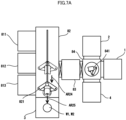
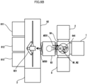
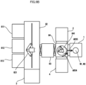
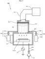
- the activation treatment device 2 is a device that generates inductively coupled plasma (ICP), and, as illustrated in FIG. 2 , includes a stage 210, a chamber 212, a plasma chamber 213, an induction coil 215 wound on the outer side of the plasma chamber 213, and a high-frequency power source 216 to supply high-frequency current to the induction coil 215.
- the plasma chamber 213 is formed of, for example, quartz glass.
- the activation treatment device 2 also includes a nitrogen gas feeder 220A and an oxygen gas feeder 220B.
- the nitrogen gas feeder 220A includes a nitrogen gas storage 221A, a feeding valve 222A, a feeding pipe 223A, and a bias applier 217.
- the oxygen gas feeder 220B includes an oxygen gas storage 221B, a feeding valve 222B, and a feeding pipe 223B.
- On the stage 210 a substrate W1 or W2 is placed.
- the chamber 212 communicates with the inside of the plasma chamber 213.
- the chamber 212 is connected to a vacuum pump 201 via an exhaust pipe 202A and an exhaust valve 203A. When the exhaust valve 203A is put into the open state and the vacuum pump 201 is caused to operate, gas in the chamber 212 is exhausted to the outside of the chamber 212 through the exhaust pipe 202A and gas pressure in the chamber 212 is reduced (decompressed).
- the high-frequency power source 216 a power source that supplies the induction coil 215 with a high-frequency current having a frequency of, for example, 27 MHz can be employed.
- a high-frequency current having a frequency of, for example, 27 MHz
- plasma PLM is formed in the plasma chamber 213. Since, on this occasion, ions contained in the plasma are trapped in the plasma chamber 213 by the induction coil 215, the activation treatment device 2 may have a configuration in which there is no trap plate at a portion between the plasma chamber 213 and the chamber 212.
- the induction coil 215, the high-frequency power source 216, and the nitrogen gas feeder 220A constitute a plasma generation source that generates plasma PLM in the plasma chamber 213 and supplies the bonding surface of the substrate W1 or W2 supported by the stage 210 with N 2 radicals in the plasma.
- the activation treatment device 2 is not limited to the example, and the activation treatment device 2 may instead be a device that includes a flat plate electrode arranged outside the plasma chamber 213, a high-frequency power source electrically connected to the flat plate electrode, and a trap plate arranged at a portion between the plasma chamber 213 and the chamber 212 and configured to trap ions in the plasma and generates capacitively coupled plasma (CCP).
- the high-frequency power source a power source that applies a high-frequency bias having a frequency of, for example, 27 MHz can be employed. Power supplied from the high-frequency power source into the plasma chamber is set to, for example, 250 W.
- the bias applier 217 is a high-frequency power source that applies a high-frequency bias to the substrate W1 or W2 supported by the stage 210.
- a power source that generates a high-frequency bias having a frequency of, for example, 13.56 MHz can be employed.
- Applying a high-frequency bias to the substrate W1 or W2 by the bias applier 217 as described above causes a sheath region in which ions with kinetic energy repeatedly collide with the substrate W1 or W2 to be generated in a vicinity of the bonding surface of the substrate W1 or W2.
- the bonding surface of the substrate W1 or W2 is etched by ions with kinetic energy existing in the sheath region.
- the activation treatment device 2 after performing the afore-described activation treatment, exposes the bonding surface of the substrate W1 or W2 to gas containing water within a preset standard time.
- the gas containing water include atmospheric air and water gas.
- a feeding pipe (not illustrated) to feed air or water gas into the chamber 212 is connected, and a feeding valve (not illustrated) is interposed in the feeding pipe.
- the activation treatment device 2 by feeding atmospheric air or water gas into the chamber 212 by putting the exhaust valve 203A into the closed state and the feeding valve into the open state, exposes the bonding surface of the substrate W1 or W2 to atmospheric air or water gas.
- a water gas feeder (not illustrated) to feed water gas into the feeding pipe is connected.
- the water gas feeder is only required to be a feeder that generates water gas by mixing carrier gas, such as argon (Ar), nitrogen (N 2 ()), helium (He), and oxygen (O 2 ()), and vaporized water and feeds the generated water gas.
- carrier gas such as argon (Ar), nitrogen (N 2 ()), helium (He), and oxygen (O 2 ()
- nitrogen is employed as a carrier gas and a gas generated by mixing 50% vaporized water with the carrier gas is employed as water gas.
- the substrate bonding device 1 bonds the substrates W1 and W2 having been subjected to the activation treatment in the activation treatment device 2 to each other.
- the substrate bonding device 1 includes a chamber 120, a stage 141, a head 142, a stage driver 143, a head driver 144, substrate heaters 1411 and 1421, and a misalignment amount measurer 150, as illustrated in FIG. 3 . Note that the following description is made appropriately assuming that the ⁇ Z-directions and an XY-direction in FIG. 3 are the vertical direction and a horizontal direction, respectively.
- the chamber 120 is connected to a vacuum pump 121 via an exhaust pipe 122B and an exhaust valve 123B.
- the stage 141 and the head 142 are arranged to face each other in the Z-direction in the chamber 120.
- the stage 141 supports the substrate W1 on the upper surface thereof, and the head 142 supports the substrate W2 on the lower surface thereof.
- the upper surface of the stage 141 and the lower surface of the head 142 may be subjected to surface roughening processing in consideration of a case where, when contact surfaces of the substrates W1 and W2 with the stage 141 and the head 142 are mirror surfaces, the substrates W1 and W2 are unlikely to be separated from the stage 141 and the head 142, respectively.
- the stage 141 and the head 142 have holding mechanisms (not illustrated) to hold the substrates W1 and W2, respectively.
- Each of the holding mechanisms includes an electrostatic chuck, a vacuum chuck, or the like.
- the stage driver 143 is capable of moving the stage 141 in an XY direction and rotating the stage 141 about the Z-axis.
- the head driver 144 causes the head 142 to ascend and descend in the vertical direction (see an arrow AR1 in FIG. 3 ).
- the head driver 144 by moving the head 142 downward, brings the head 142 close to the stage 141.
- the head driver 144 by moving the head 142 upward, separates the head 142 away from the stage 141.
- the head driver 144 applies drive force to the head 142 in a direction in which the head 142 comes close to the stage 141 while the substrates W1 and W2 are in contact with each other, the substrate W2 is pressed against the substrate W1.
- a pressure sensor 148 to measure drive force that the head driver 144 applies to the head 142 in a direction in which the head 142 comes close to the stage 141 is disposed.
- the pressure sensor 148 is, for example, a load cell, and pressure exerted on the bonding surfaces of the substrates W1 and W2 when the substrate W2 is pressed against the substrate W1 by the head driver 144 can be detected from a measured value detected by the load cell.
- the substrate heaters 1411 and 1421 respectively include, for example, electrothermal heaters.
- the substrate heaters 1411 and 1421 heat the substrates W1 and W2 by transmitting heat to the substrates W1 and W2 supported by the stage 141 and the head 142, respectively.
- the substrate heaters 1411 and 1421 is capable of adjusting the temperature of the substrates W1 and W2 or the bonding surfaces thereof by adjusting the amounts of heat generation by the substrate heaters 1411 and 1421, respectively.
- the misalignment amount measurer 150 by recognizing positions of marks for position alignment (alignment marks) that are disposed on the respective ones of the substrates W1 and W2, measures a misalignment amount in a horizontal direction of the substrate W1 with respect to the substrate W2.
- the misalignment amount measurer 150 recognizes the alignment marks of the substrates W1 and W2, using, for example, light (for example, infrared light) transmitted through the substrates W1 and W2.
- the stage driver 143 by moving the stage 141 in a horizontal direction or rotating the stage 141, based on a misalignment amount measured by the misalignment amount measurer 150, executes mutual positioning operation (alignment operation) between the substrates W1 and W2. Both the measurement of a misalignment amount by the misalignment amount measurer 150 and the alignment operation by the stage driver 143 are executed under the control of the controller 9.
- the controller 9 is, for example, a programmable logic controller.
- the controller 9 calculates pressure at the time of bringing the substrates W1 and W2 into pressure contact with each other and calculates a relative misalignment amount between the substrates W1 and W2, based on measurement signals input from the pressure sensor, the misalignment amount measurer 150, and the like.
- the controller 9 controls the operation of the stage driver 143 and the head driver 144, by outputting control signals to the stage driver 143 and the head driver 144, based on the calculated pressure or misalignment amount.
- controller 9 by outputting control signals to the substrate heaters 1411 and 1421, the high-frequency power source 216, the bias applier 217, the feeding valves 222A and 222B, and the transportation robots 821 and 841, controls the operation thereof.
- FIGS. 4A to 9 a flow of operation from when the substrates W1 and W2 are input to the substrate bonding system to when the substrates W1 and W2 have been bonded to each other and are taken out from the substrate bonding system is described referring to FIGS. 4A to 9 .
- the substrates W1 and W2 are first arranged on the feeding ports 811 and 812 illustrated in FIG. 4A , respectively.
- the substrates W1 and W2 are formed of one of, for example, a Si substrate, a glass substrate, an oxide substrate (for example, a silicon oxide (SiOz) substrate or an alumina substrate (Al 2 O 3 )), and a nitride substrate (for example, silicon nitride (SiN) or aluminum nitride (AlN)).
- a Si substrate for example, a silicon substrate (SiOz) substrate or an alumina substrate (Al 2 O 3 )
- a nitride substrate for example, silicon nitride (SiN) or aluminum nitride (AlN).
- at least one of the substrates W1 and W2 may be a substrate on the bonding surface of which a metal portion and an insulating film are exposed.
- at least one of the substrates W1 and W2 may be a substrate on the bonding surface of which an insulating film formed by depositing an oxide or a nitride is exposed.
- the description is made assuming that the substrate W1 is a glass substrate or an oxide substrate and the substrate W2 is a Si substrate or a nitride substrate.
- the substrate W2 to be held by the head 142 in the substrate bonding device 1 is arranged, and, on the feeding port 812, for example, the substrate W1 to be placed on the stage 141 in the substrate bonding device 1 is arranged.
- the transportation robot 821 takes the substrate W2 out of the feeding port 811, as illustrated by an arrow AR11 in FIG. 4A .
- the transportation robot 821 while holding the substrate W2, moves to a position in the first transportation device 82 at which the transportation robot 821 carries the substrate W2 into the load lock chamber 83, as illustrated by an arrow AR12 in FIG. 4A .
- the transportation robot 821 when the substrate W1 is arranged on the feeding port 812, after taking out the substrate W1 from the feeding port 812, the transportation robot 821, while holding the substrate W1, moves to a position in the first transportation device 82 at which the transportation robot 821 carries the substrate W1 into the load lock chamber 83.
- a door on the first transportation device 82 side of the load lock chamber 83 is opened and, at the same time, the transportation robot 821 turns in such a way that the tip portion of the arm points to the load lock chamber 83 side, as illustrated by an arrow AR13 in FIG. 4A .
- the transportation robot 821 by stretching the arm, inserts the tip portion of the arm into the load lock chamber 83, as illustrated by an arrow AR14 in FIG. 4B .
- the substrate W1 or W2 is transferred from the tip portion of the arm to the stage in the load lock chamber 83.
- the transportation robot 821 contracts the arm, as illustrated by an arrow AR15 in FIG. 5A . Then, the door on the first transportation device 82 side of the load lock chamber 83 is closed.
- the transportation robot 841 while pointing the tip portion of the arm to the load lock chamber 83 side, stretches the arm.
- the transportation robot 841 by contracting the arm, takes the substrate W1 or W2 out of the load lock chamber 83, as illustrated by an arrow AR16 in FIG. 5A .
- the door on the second transportation device 84 side of the load lock chamber 83 is closed.
- the transportation robot 841 turns in such a way that the tip portion of the arm points to the activation treatment device 2 side, as illustrated by an arrow AR17 in FIG. 5B , and, at the same time, the activation treatment device 2 opens a carrying in/out port for the substrate W1 or W2.
- the transportation robot 841 by stretching the arm, inserts the tip portion of the arm into the activation treatment device 2.
- the substrate W1 or W2 is transferred from the tip portion of the arm of the transportation robot 841 to the stage 210 (see FIG. 2 ) in the activation treatment device 2.
- the activation treatment device 2 closes the carrying in/out port for the substrate W1 or W2.
- the activation treatment device 2 by subjecting at least one of the bonding surfaces to be bonded to each other of the respective ones of the substrates W1 and W2 to at least one of reactive ion etching using nitrogen gas and irradiation of nitrogen radicals, performs an activation treatment step of activating the bonding surface.
- the activation treatment device 2 uses a different processing sequence depending on the type of substrate to be processed in the activation treatment of the bonding surface.
- the activation treatment device 2 When the activation treatment device 2 subjects the bonding surface of the substrate W1, that is, a glass substrate or an oxide substrate, to the activation treatment, the activation treatment device 2 first feeds N 2 gas into the chamber 212 from the nitrogen gas storage 221A through the feeding pipe 223A by opening the feeding valve 222A illustrated in FIG. 2 . Next, the activation treatment device 2, while supply of high-frequency current from the high-frequency power source 216 to the induction coil 215 is stopped, applies high-frequency bias to the substrate W1 or W2 placed on the stage 210 by the bias applier 217. Through this processing, the bonding surface of the substrate W1 is subjected to reactive ion etching (RIE) using N 2 gas.
- RIE reactive ion etching
- the activation treatment device 2 starts supply of the high-frequency current from the high-frequency power source 216 to the induction coil 215 and thereby generates plasma with the N 2 gas.
- the activation treatment device 2 stops application of the high-frequency bias to the substrate W1 by the bias applier 217. In this way, the bonding surface of the substrate W1 is irradiated with N 2 radicals.
- the activation treatment device 2 subjects the bonding surface of the substrate W2, that is, a Si substrate or a nitride substrate, to the activation treatment
- the activation treatment device 2 first feeds Oz gas into the chamber 212 from the oxygen gas storage 221B through the feeding pipe 223B by opening the feeding valve 222B.
- the activation treatment device 2 while supply of high-frequency current from the high-frequency power source 216 to the induction coil 215 is stopped, applies a high-frequency bias to the substrate W2 placed on the stage 210 by the bias applier 217.
- the bonding surface of the substrate W2 is subjected to reactive ion etching (RIE) using Oz gas.
- RIE reactive ion etching
- the activation treatment device 2 by closing the feeding valve 222B and thereby stopping feeding of O 2 gas from the Oz gas storage 221B into the chamber 212, exhausts the Oz gas in the chamber 212. Subsequently, the activation treatment device 2 feeds N 2 gas into the chamber 212 from the nitrogen gas storage 221A through the feeding pipe 223A by opening the feeding valve 222A. Subsequently, the activation treatment device 2 starts supply of the high-frequency current from the high-frequency power source 216 to the induction coil 215 and thereby generates plasma with the N 2 gas. On this occasion, the activation treatment device 2 stops application of the high-frequency bias to the substrate W2 by the bias applier 217.
- the bonding surface of the substrate W2 is irradiated with N 2 radicals.
- the activation treatment device 2 performs a gas exposure step of exposing the bonding surface of the substrate W1 or W2 to atmospheric air or water gas within a preset standard time. Then, the activation treatment device 2 opens the carrying in/out port for the substrate W1 or W2.
- the transportation robot 841 stretches the arm and inserts the tip portion of the arm into the activation treatment device 2, and the substrate W1 or W2 is transferred from the stage 210 to the tip portion of the arm.
- the transportation robot 841 by contracting the arm, takes the substrate W1 or W2 out of the activation treatment device 2, as illustrated by an arrow AR19 in FIG. 6A .
- the transportation robot 841 turns in such a way that the tip portion of the arm points to the load lock chamber 83 side as illustrated by an arrow AR20 in FIG. 6A , the door on the second transportation device 84 side of the load lock chamber 83 is opened.
- the transportation robot 841 stretches the arm and inserts the tip portion of the arm into the load lock chamber 83, and the substrate W1 or W2 is transferred from the tip portion of the arm to the stage in the load lock chamber 83.
- the transportation robot 841 contracts the arm as illustrated by an arrow AR21 in FIG. 6B , and, at the same time, the door on the second transportation device 84 side of the load lock chamber 83 is closed.
- the transportation robot 821 while pointing the tip portion of the arm to the load lock chamber 83 side, stretches the arm and inserts the tip portion of the arm into the load lock chamber 83. Then, the substrate W1 or W2 is transferred from the stage in the load lock chamber 83 to the tip portion of the arm of the transportation robot 821. Subsequently, after the transportation robot 821, by contracting the arm, takes the substrate W1 or W2 out of the load lock chamber 83 as illustrated by an arrow AR22 in FIG. 6B , the door on the first transportation device 82 side of the load lock chamber 83 is closed.
- the transportation robot 821 turns in such a way that the tip portion of the arm points to the cleaning device 3 side, as illustrated by an arrow AR23 in FIG. 6B .
- the transportation robot 821 while holding the substrate W1 or W2, moves to a position in the first transportation device 82 at which the transportation robot 821 carries the substrate W1 or W2 into the cleaning device 3, as illustrated by an arrow AR24 in FIG. 7A .
- the cleaning device 3 opens a carrying in/out port for the substrate W1 or W2
- the transportation robot 821 by stretching the arm, inserts the tip portion of the arm into the cleaning device 3.
- the substrate W1 or W2 is transferred from the tip portion of the arm of the transportation robot 821 to the stage in the cleaning device 3.
- the cleaning device 3 while spraying water to which ultrasonic waves are applied on the bonding surface of the substrate W1 or W2 from the cleaning head, causes the stage on which the substrate W1 or W2 is placed to scan in XY directions and cleans the entire bonding surface of the substrate W1 or W2. Through this processing, foreign objects having adhered to the bonding surface of the substrate W1 or W2 are removed. Succeedingly, the cleaning device 3 stops the discharge of water by the cleaning head and subsequently, by spin-drying the substrate by rotating the stage, finishes the cleaning treatment. Subsequently, when a sequence of cleaning processing described above is finished, the cleaning device 3 opens the carrying in/out port for the substrate W1 or W2.
- the transportation robot 821 stretches the arm and inserts the tip portion of the arm into the cleaning device 3, and the substrate W1 or W2 is transferred from the stage to the tip portion of the arm.
- the transportation robot 821 by contracting the arm, takes the substrate W1 or W2 out of the cleaning device 3, as illustrated by an arrow AR26 in FIG. 7B .
- the transportation robot 821 while holding the substrate W1 or W2, moves to the position in the first transportation device 82 at which the transportation robot 821 carries the substrate W1 or W2 into the load lock chamber 83, as illustrated by an arrow AR27 in FIG. 7B .
- the door on the first transportation device 82 side of the load lock chamber 83 is opened and, at the same time, the transportation robot 821 turns in such a way that the tip portion of the arm points to the load lock chamber 83 side, as illustrated by an arrow AR28 in FIG. 7B .
- the transportation robot 821 by stretching the arm, inserts the tip portion of the arm into the load lock chamber 83, as illustrated by an arrow AR29 in FIG. 8A . Then, the substrate W1 or W2 is transferred from the tip portion of the arm to the stage in the load lock chamber 83. Succeedingly, when the transfer of the substrate W1 or W2 to the stage in the load lock chamber 83 is finished, the transportation robot 821 contracts the arm, as illustrated by an arrow AR30 in FIG. 8B . Then, the door on the first transportation device 82 side of the load lock chamber 83 is closed.
- the transportation robot 841 while pointing the tip portion of the arm to the load lock chamber 83 side, stretches the arm.
- the transportation robot 841 by contracting the arm, takes the substrate W1 or W2 out of the load lock chamber 83, as illustrated by an arrow AR31 in FIG. 8B .
- the door on the second transportation device 84 side of the load lock chamber 83 is closed.
- the transportation robot 841 takes out of the load lock chamber 83 the substrate W2 that is to be supported by the head 142 in the substrate bonding device 1, the transportation robot 841 turns in such a way that the tip portion of the arm points to the turnover device 4 side, as illustrated by an arrow AR32 in FIG. 9A .
- the transportation robot 841 by stretching the arm, inserts the tip portion of the arm into the turnover device 4.
- the substrate W2 is transferred from the tip portion of the arm of the transportation robot 841 to the substrate holder in the turnover device 4. Subsequently, the transportation robot 841 contracts the arm.
- the turnover device 4 by turning over the substrate holder, holds the substrate W2 in such an attitude that the bonding surface of the substrate W2 faces vertically downward.
- the transportation robot 841 by stretching the arm, inserts the tip portion of the arm into the turnover device 4 and, while holding the opposite side to the bonding surface side of the substrate W2, takes the substrate W2 out of the turnover device 4.
- the transportation robot 841 turns in such a way that the tip portion of the arm points to the substrate bonding device 1 side, as illustrated by an arrow AR34 in FIG. 9B .
- the transportation robot 841 takes out of the load lock chamber 83 the substrate W1 that is to be placed on the stage 141 in the substrate bonding device 1, the transportation robot 841 directly turns in such a way that the tip portion of the arm points to the substrate bonding device 1 side.
- the transportation robot 841 when the substrate bonding device 1 opens a carrying in/out port for the substrate W1 or W2, the transportation robot 841, by stretching the arm, inserts the tip portion of the arm into the substrate bonding device 1. Then, as illustrated by an arrow AR35 in FIG. 9B , the substrate W2 is transferred from the tip portion of the arm of the transportation robot 841 to the head 142 (see FIG. 3 ) in the substrate bonding device 1, or the substrate W1 is transferred from the tip portion of the arm of the transportation robot 841 to the stage 141 (see FIG. 3 ) in the substrate bonding device 1. Succeedingly, when the transportation robot 841 contracts the arm, the substrate bonding device 1 closes the carrying in/out port for the substrate W1 or W2.
- the substrate bonding device 1 by putting the exhaust valve 123B into the closed state, reduces air pressure in the chamber 120. Note that, as described afore, a step in which the substrate W1 or W2 is transported through the first transportation device 82, the second transportation device 84, and the load lock chamber 83 is equivalent to a transportation step.
- the substrate bonding device 1 performs a bonding step of bonding two substrates having the bonding surfaces having been subjected to the activation treatment in the activation treatment step to each other.
- the substrate bonding device 1 moves the substrate W2 in a direction in which, from a state in which the substrates W1 and W2 are separated from each other, the substrates W1 and W2 come close to each other and brings the bonding surfaces of the substrates W1 and W2 into contact with each other.
- the substrate bonding device 1 first brings the head 142 supporting the substrate W2 close to the stage 141 supporting the substrate W1 and thereby causes both substrates W1 and W2 to come close to each other.
- the substrate bonding device 1 executes alignment operation of both substrates W1 and W2, based on a misalignment amount measured by the misalignment amount measurer 150.
- the substrate bonding device 1 by bringing the head 142 close to the stage 141 again, causes the two substrates W1 and W2 to come into contact with each other.
- the substrate bonding device 1 while keeping the bonding surfaces of the substrates W1 and W2 in contact with each other, bonds the two substrates W1 and W2 to each other by applying pressure in a direction in which the two substrates W1 and W2 adhere to each other.
- the bonding surfaces of the substrates W1 and W2 are covered by OH groups or water molecules. Because of this condition, bringing the bonding surfaces of the substrates W1 and W2 into contact with each other causes the substrates W1 and W2 to be temporarily bonded to each other by hydrogen bonds between OH groups or water molecules.
- the substrate bonding device 1 maintains the substrates W1 and W2 in a heated state at, for example, 120 to 200°C by the substrate heaters 1411 and 1421, respectively, for 2 to 7 hours. It is considered that, through this heating, many of water molecules and hydrogen generated at the time when hydrogen bonds between OH groups existing on the bonding surfaces of the substrates W1 and W2 are converted to covalent bonds or water molecules and hydrogen remaining on the bonding surfaces of the substrates W1 and W2 even in a vacuum get out of a bonding interface between the substrates W1 and W2 to the outside and strong covalent bonds are formed between the bonding surfaces.
- the bonding surfaces of the substrates W1 and W2 come into contact with each other even in a portion that was not in contact at the time of temporary bonding, that is, the bonding interface extends in effect, and, as a result, bonding area increases.
- the substrate bonding device 1 When the substrate bonding device 1 has bonded the substrates W1 and W2 to each other, the substrate bonding device 1, by putting the exhaust valve 123B into the closed state and the air feeding valve into the open state and thereby feeding air into the chamber 120, brings air pressure in the chamber 120 to an atmospheric pressure. Then, the substrate bonding device 1 opens the carrying in/out port for the substrates W1 and W2.
- the transportation robot 841 illustrated in FIG. 9B by stretching the arm, inserts the tip portion of the arm into the substrate bonding device 1. Then, the substrates W1 and W2 that are bonded to each other are transferred from the stage 141 or the head 142 in the substrate bonding device 1 to the tip portion of the arm of the transportation robot 841.
- the transportation robot 841 by contracting the arm, takes the substrates W1 and W2 bonded to each other out of the substrate bonding device 1. Then, the substrate bonding device 1 closes the carrying in/out port for the substrates W1 and W2 again. Succeedingly, the transportation robot 841 turns in such a way that the tip portion of the arm points to the load lock chamber 83 side.
- the transportation robot 841 while pointing the tip portion of the arm to the load lock chamber 83 side, stretches the arm.
- the transportation robot 841 contracts the arm. Then, the door on the second transportation device 84 side of the load lock chamber 83 is closed.
- the transportation robot 821 After the door on the first transportation device 82 side of the load lock chamber 83 is opened, the transportation robot 821, while pointing the tip portion of the arm to the load lock chamber 83 side, stretches the arm and inserts the tip portion of the arm into the load lock chamber 83. Then, the substrates W1 and W2 bonded to each other are transferred from the stage in the load lock chamber 83 to the tip portion of the arm of the transportation robot 821. Subsequently, after the transportation robot 821, by contracting the arm, takes the substrates W1 and W2 bonded to each other out of the load lock chamber 83, the door on the first transportation device 82 side of the load lock chamber 83 is closed.
- the transportation robot 821 turns in such a way that the tip portion of the arm points to the opposite side to the load lock chamber 83 side. Subsequently, the transportation robot 821, while holding the substrates W1 and W2 bonded to each other, moves to a position in the first transportation device 82 at which the transportation robot 821 carries the substrates W1 and W2 bonded to each other into the take-out port 813. Next, the transportation robot 821, by stretching the arm, inserts the tip portion of the arm into the take-out port 813 and arranges the substrates W1 and W2 bonded to each other in the take-out port 813.
- the flow rate of the Oz gas fed into the chamber 212 was set to 50 sccm
- the bias power of a high-frequency bias applied to the substrate W2 was set to 110 W
- treatment time was set to 30 sec.
- the flow rate of N 2 gas fed into the chamber 212 was set to 200 sccm
- power supplied to the induction coil 215 was set to 2500 W
- treatment time was set to 15 sec.
- Table 1 below shows a list including an exposure medium to which the bonding surfaces of the substrates W1 and W2 were exposed and a location at which the substrates W1 and W2 were first exposed to the exposure medium after the activation treatment was finished for each of Samples 1 to 4 among 20 types of samples.
- a SiO 2 substrate and a Si substrate were used as the substrate W1 and the substrate W2, respectively.
- the SiO 2 substrate a thermal oxide film substrate in which a SiO 2 film is formed on a surface of a Si substrate was employed.
- Activation treatment device indicates that, after the activation treatment in the activation treatment device 2 was finished, the bonding surface of the substrate W1 or W2 was exposed to an exposure medium in the activation treatment device 2 without moving therefrom
- Second transportation device indicates that, after the activation treatment in the activation treatment device 2 was finished, the transportation robot 841 took the substrate W1 or W2 out of the activation treatment device 2 to the second transportation device 84 and the substrate W1 or W2 was exposed to an exposure medium in the second transportation device 84.
- “Load lock chamber” indicates that, after the activation treatment in the activation treatment device 2 was finished, the transportation robot 841 took the substrate W1 or W2 out of the activation treatment device 2 and subsequently carried the substrate W1 or W2 into the load lock chamber 83, and the substrate W1 or W2 was exposed to an exposure medium in the load lock chamber 83.
- the substrate W1 after having been subjected to the RIE treatment using N 2 gas, was subjected to the N 2 radical treatment, and the substrate W2, after having been subjected to the RIE treatment using Oz gas, was subjected to the N 2 radical treatment.
- Table 2 shows a list including a time from when the activation treatment on the substrate W1 or W2 was finished until when the substrate W1 or W2 was exposed to atmospheric air for each of Samples 5 to 7 among the 20 types of samples. Note that, for all Samples 5 to 7, in the activation treatment device 2, the substrate W1, after having been subjected to the RIE treatment using N 2 gas, was subjected to the N 2 radical treatment, and the substrate W2, after having been subjected to the RIE treatment using Oz gas, was subjected to the N 2 radical treatment. [Table 2] Time to atmospheric air exposure after activation treatment [min] Sample 5 1 Sample 6 5 Sample 7 10
- Table 3 shows a list including details of the activation treatment on the substrates W1 and W2 and a time from when the activation treatment was finished until when the substrate W1 or W2 was exposed to atmospheric air for each of Samples 2 and 8 to 9 among the 20 types of samples.
- “Substrate W1” and “Substrate W2” in Table 3 indicate details of the activation treatment on the substrate W1 and details of the activation treatment on the substrate W2, respectively.
- N 2 RIE treatment "N 2 radical treatment”, and “Oz RIE treatment”
- Done indicates that the treatment was performed
- “Not done” indicates that the treatment was omitted.
- N 2 RIE treatment and “Oz RIE treatment” indicate the RIE treatment using N 2 gas and the RIE treatment using Oz gas, respectively.
- Substrate W1 Substrate W2 Time to atmospheric air exposure after activation treatment [min] O 2 RIE treatment N 2 RIE treatment N 2 radical treatment 0 2 RIE treatment N 2 radical treatment Sample 2 Not done Done Done Done Done 0 Sample 8 Not done Done Not done Done Not done 0 Sample 9 Done Not done Not done Done Not done 0 Sample 10 Done Not done Not done Done Not done 10
- Table 4 shows a list including a gas pressure condition in the second transportation device 84, the load lock chamber 83, and the first transportation device 82 at the time when the substrate W1 or W2 was transported from the activation treatment device 2 to the cleaning device 3 for each of Samples 2 and 11 to 14 among the 20 types of samples.
- Gas pressure during transportation [Pa] Sample 11 10000 Sample 2 1000 Sample 12 100 Sample 13 10 Sample 14 1
- Table 5 below shows a list including details of the activation treatment on the substrates W1 and W2 for each of Samples 15 to 18 among the 20 types of samples. Note that, in Samples 15 to 18, both substrates W1 and W2 are glass substrates.
- N 2 RIE treatment "N 2 radical treatment”, and “Oz RIE treatment” in Table 5 are the same as those in Table 3.
- the flow rate of the N 2 gas fed into the chamber 212 was set to 50 sccm
- the bias power of a high-frequency bias applied to the substrate W1 was set to 250 W
- treatment time was set to 60 sec.
- Table 6 below shows a list including details of the activation treatment on the substrates W1 and W2 for each of Samples 19 and 20 among the 20 types of samples.
- the substrates W1 and W2 were exposed to water gas after the activation treatment.
- both substrates W1 and W2 are substrates in each of which, on a Si substrate, an insulating film formed by depositing SiOz is formed.
- the flow rate of the N 2 gas fed into the chamber 212 was set to 50 sccm
- the bias power of a high-frequency bias applied to the substrate W1 was set to 500 W
- treatment time was set to 60 sec.
- Table 7 shows a list including details of the activation treatment on the substrates W1 and W2 for each of Samples 21 and 22 among the 22 types of samples.
- both substrates W1 and W2 are glass substrates the bonding surfaces of which have a surface roughness of 0.49 nm in RMS.
- N 2 RIE treatment "N 2 radical treatment”, and "Oz RIE treatment” in Table 7 are the same as those in Table 3.
- the flow rate of the N 2 gas fed into the chamber 212 was set to 50 sccm
- the bias power of a high-frequency bias applied to the substrate W1 was set to 250 W
- treatment time was set to 120 sec.
- the flow rate of the Oz gas fed into the chamber 212 was set to 50 sccm
- the bias power of a high-frequency bias applied to the substrates W1 and W2 was set to 250 W
- treatment time was set to 120 sec.
- N 2 radical treatment on the substrates W1 and W2 a configuration including flat plate electrodes arranged outside the plasma chamber 213 and a high-frequency power source connected to the flat plate electrodes was used, and the flow rate of N 2 gas fed into the plasma 213 was set to 200 sccm, power supplied between the flat plate electrodes was set to 250 W at 27MHz, and treatment time was set to 15 sec.
- the bonding processing of the substrates W1 and W2 in the substrate bonding device 1 for any samples was performed by, while gas pressure in the chamber 120 is set to 1000 Pa, temporarily bonding the substrates W1 and W2 to each other by applying a pressure of 1000 N and subsequently performing heat treatment under the conditions of a treatment temperature of 200°C and a treatment time of 2 hours.
- gas pressure in the chamber 120 is set to 1000 Pa
- temporarily bonding the substrates W1 and W2 to each other by applying a pressure of 1000 N and subsequently performing heat treatment under the conditions of a treatment temperature of 200°C and a treatment time of 2 hours.
- the evaluation of bonding strength between the substrates W1 and W2 for each of Samples 1 to 22 was performed by measuring bonding strength (in terms of surface energy) using a crack and opening method that is performed by inserting a blade.
- bonding strength in terms of surface energy
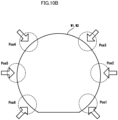
- the crack and opening method first, peel length L of two substrates W1 and W2 bonded to each other at the time when a blade BL like, for example, a blade of a razor is inserted into a bonded portion of the substrates W1 and W2 from the periphery of the substrates W1 and W2 as illustrated by an arrow in FIG. 10A is measured.
- a blade BL for example, a blade with a thickness of 100 ⁇ m is used.
- Y indicates Young's modulus
- Ts indicates thickness of the substrates W1 and W2
- Tb indicates thickness of the blade BL.
- the Young's modulus Y was set to 6.5 ⁇ 10 10 N/m 2
- the thickness Ts of the substrates W1 and W2 was set to 0.0011 m (1.1 mm)
- the thickness Tb of the blade BL was set to 0.0001 m (0.1 mm). According to the computation formula, the shorter the peel length is, the larger the bonding strength becomes.
- a bonding strength of less than 1 J/m 2 means an insufficient strength and the bonding strength is required to be greater than or equal to 1 J/m 2
- a bonding strength of 1.5 J/m 2 or more is a magnitude that enables a bonded product to be generally determined to be a non-defective product
- peel lengths are also included in the table.
- each value in the column “Bonding strength (in terms of surface energy)” indicates an average value of bonding strengths (in terms of surface energy) at the six positions ("Pos1" to "Pos6") on the peripheral portion of the two substrates W1 and W2 illustrated in FIG. 10B , and, for a sample where bulk fractures occurred at all the six positions on the peripheral portion of the two substrates W1 and W2, an estimated bonding strength is included.
- each value in the column “Number of bulk fractured positions” indicates the number of positions at which a bulk fracture occurred among the six positions on the peripheral portion of the two substrates W1 and W2.
- the bonding strengths (in terms of surface energy) were greater than or equal to 2.5 J/m 2 and five positions at which the bonding strength reached the bulk fracture strength existed.
- the substrate W2 which is formed of a Si substrate, does not have a native oxide film formed on the bonding surface, an oxide film is formed on the bonding surface by performing the Oz RIE treatment.
- the substrate W2 since the bonding surface thereof is subjected to the N 2 radical treatment even when the N 2 RIE treatment is omitted, it is considered that the bonding surface is in the afore-described N-activated state.
- time required from when the activation treatment in the activation treatment device 2 is finished to when the substrates W1 and W2 are exposed to atmospheric air on the second transportation device 84 is approximately 5 min and time required from when the activation treatment is finished to when the substrates W1 and W2 are exposed to atmospheric air in the load lock chamber 83 is approximately 10 min, and, based on this result, it is found that the longer the time required from when the activation treatment is finished to when the substrates W1 and W2 are exposed to atmospheric air becomes, the lower the bonding strength between the substrates W1 and W2 becomes.
- the bonding strength improved as the gas pressure at the time of transportation increased in such a manner that: when the gas pressure was 1 Pa, the bonding strength was low at 0.81 J/m 2 ; when the gas pressure was 10 Pa, the bonding strength was 1.55 J/m 2 ; when the gas pressure was 100 Pa, the bonding strength was 2.15 J/m 2 ; when the gas pressure was 1000 Pa, the bonding strength was 2.89 J/m 2 ; and when the gas pressure was 10000 Pa, the bonding strength was 2.98 J/m 2 .
- the bonding strength was 2.98 J/m 2 .
- performing the O 2 RIE treatment before performing the N 2 RIE treatment caused wettability between the substrates W1 and W2 to be improved and the bonding strength between the substrates W1 and W2 to be improved and, at the same time, the number of voids occurring between the substrates W1 and W2 to be reduced. It is considered that this is because adhering substances, such as organic substances, that have adhered to the bonding surfaces of the substrates W1 and W2 being removed by the O 2 RIE treatment caused a larger number of OH groups to be formed on the bonding surfaces of the substrates W1 and W2 that were in the N-activated state in the subsequent N 2 RIE treatment and N 2 radical treatment. It is also considered that organic substances that have adhered to the bonding surfaces of the substrates W1 and W2 being removed by the O 2 RIE treatment caused wettability of the bonding surfaces of the substrates W1 and W2 to be increased.
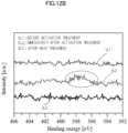
- the activation treatment caused SiON that is an oxynitride to be formed on the bonding surfaces of the substrates W1 and W2.
- the substrates W1 and W2 after activation treatment were subjected to heat treatment under the same conditions as the conditions for heat treatment for Samples 21 and 22, disappearance of the N1s peak was confirmed, as illustrated by curves SL2 and SL3 in FIG. 12B .
- the bonding strength of Sample 22 is substantially improved compared with the bonding strength of Sample 21, it is considered that, in Sample 22, the oxynitride (SiON) is replaced by OH groups that contribute to hydrogen bonds in the bonded portion between the substrates W1 and W2.
- the bonding surfaces to be bonded to each other of the respective ones of the two substrates W1 and W2 are activated by subjecting the bonding surfaces of the substrates W1 and W2 to the reactive ion etching using nitrogen gas and the irradiation of nitrogen radicals.
- the N-activated state of the bonding surfaces of the substrates W1 and W2 that is formed by this activation is unstable, and, when left untreated, the bonding strength is reduced because the activated state is to be deactivated.
- the bonding surfaces of the substrates W1 and W2 are required to be brought into contact with water molecules within a predetermined standard time after having been activated.
- the bonding surfaces of the substrates W1 and W2 are exposed to atmospheric air or water gas within a predetermined standard time after the bonding surfaces of the substrates W1 and W2 are activated. Since this processing enables the bonding surfaces of the substrates W1 and W2 to come into contact with water molecules while being N-activated, a large number of oxynitrides can be formed on the bonding surfaces of the substrates W1 and W2.
- OH groups are generated only after the substrates W 1 and W2 are subjected to heat treatment after having been temporarily bonded to each other and the bonding strength between the substrates W1 and W2 is thereby improved.
- the substrate bonding method according to the present embodiment by bringing the bonding surfaces of the substrates W 1 and W2 into contact with water molecules while a large number of oxynitrides (N groups) have been generated on the bonding surfaces by subjecting the bonding surfaces of the substrates W 1 and W2 to the activation treatment, a large number of oxynitrides (N groups) on the bonding surfaces of the substrates W1 and W2 are respectively replaced by OH groups.
- the present embodiment relates to an invention of a method for generating a large number of OH groups on the bonding surfaces of the substrates W1 and W2 at a stage before subjecting the bonding surfaces of the substrates W1 and W2 to heat treatment after having subjected the bonding surfaces of the substrates W1 and W2 to the activation treatment.
- bonding surfaces are cleaned by spraying water on the bonding surfaces after wettability of the bonding surfaces is increased by subjecting the bonding surfaces of the substrates to RIE treatment, and subsequently the substrates are temporarily bonded to each other by bringing the bonding surfaces of the two substrates into contact with each other with water molecules interposed between the bonding surfaces of the substrates under atmospheric pressure.
- OH groups are formed on the bonding surfaces of the substrates W1 and W2 in the activation treatment, as illustrated in section (C-1) of FIG. 13 .
- section (C-2) of FIG. 13 a state in which a comparatively large number of OH groups are formed on the bonding surfaces of the substrates W1 and W2 is maintained, as illustrated in section (C-2) of FIG. 13 . Therefore, performing heat treatment after the two substrates are temporarily bonded to each other through hydrogen bonding via OH groups causes the two substrates to be bonded to each other via strong covalent bonds, as illustrated in section (C-3) of FIG. 13 .
- the substrate bonding system according to the present embodiment As indicated by the afore-described evaluation result of bonding strength, performing heat treatment after the substrates W1 and W2 are temporarily bonded to each other under the conditions of a treatment temperature of 150°C and a treatment time of 7 hours enables a high bonding strength to be achieved. In other words, even when the treatment temperature of heat treatment is set to 150°C or less, it is possible to secure a high bonding strength.
- the substrates W1 and W2 were transported from the second transportation device 84 to the load lock chamber 83 under reduced pressure and were subsequently exposed to atmospheric air. In this case, approximately 10 min elapsed before the substrates W1 and W2 were exposed to atmospheric air, and sufficient bonding strength was not able to be achieved.
- the substrate bonding system according to the present embodiment by exposing the substrates W1 and W2 to atmospheric air in the activation treatment device 2 or the second transportation device 84 after the activation treatment in the activation treatment device 2 is finished, time required from the finish of activation treatment to atmospheric air exposure is reduced, and the bonding strength between the substrates W1 and W2 can be increased.
- the bonding strength between the substrates W1 and W2 can be further increased.
- the inside of the chamber 212 was once brought into a reduced pressure state and, after having been transported to the load lock chamber 83 under reduced pressure, the substrates W1 and W2 were exposed to atmospheric air in order to input the substrates W1 and W2 to the cleaning device 3, a bulk fracture occurred and there was no large difference in the bonding strength between the substrates W1 and W2.
- the substrates W1 and W2 were transported from the cleaning device 3 to the substrate bonding device 1, the substrates W1 and W2 were transported under a reduced pressure of approximately 1 Pa and bonding of the substrates W1 and W2 to each other was performed under a pressure of approximately 1 Pa in the substrate bonding device 1.
- the substrates W1 and W2 are transported from the cleaning device 3 to the substrate bonding device 1 under a pressure of 10 Pa or more and 1000 Pa or less. Because of this configuration, evaporation of water molecules adhering to the substrates W1 and W2 is prevented and bonding strength between the substrates W1 and W2 can be increased.
- the substrate bonding system may be a substrate bonding system including a water gas feeder (not illustrated) to feed water gas into the load lock chamber 83 or the second transportation device 84.
- the water gas feeder generates water gas by mixing carrier gas, such as argon (Ar), nitrogen (N 2 ), helium (He), and oxygen (Oz), and vaporized water and feeds the generated water gas.
- carrier gas such as argon (Ar), nitrogen (N 2 ), helium (He), and oxygen (Oz)
- the water gas feeder is connected to the load lock chamber 83 via a feeding valve and a feeding pipe.
- the flow rate of water gas and carrier gas to be fed into the load lock chamber 83 is adjusted by controlling an opening degree of the feeding valve.
- the water gas feeder may have a configuration in which molecules or clusters of molecules of water (H 2 O) are accelerated and radiated toward the bonding surfaces of the substrate W1 or W2.
- the water gas feeder may include a particle beam source to emit accelerated water (H 2 O) particles.
- the particle beam source may have a configuration in which water gas is generated using, for example, an ultrasonic wave generation element.
- the water gas feeder is only required to have a configuration to generate a particle beam of water by feeding the afore-described mixed gas of carrier gas and water (H 2 O) generated by bubbling or ultrasonic waves to the afore-described particle beam source and radiate the generated particle beam to the bonding surfaces of the substrates W1 and W2.
- the load lock chamber 83 may be opened to atmospheric air after the bonding surfaces of the substrates W1 and W2 are exposed to water gas in the load lock chamber 83 without opening the load lock chamber 83 to atmospheric air.
- a gas containing H or OH groups may be fed to the bonding surfaces of the substrates W1 and W2.
- the activation treatment device may be an activation treatment device including a particle beam source to, by irradiating the substrates W1 and W2 with a particle beam, activate the bonding surfaces of the substrates W1 and W2.
- An activation treatment device 3002 includes a chamber 3212, a stage 3210 to hold the substrate W1 or W2, a particle beam source 3061, and a beam source transporter 3063, as illustrated in, for example, FIG. 14 . Note that, in FIG. 14 , the same reference signs as those in FIG. 2 are assigned to the same constituent components as those in the embodiment.
- the activation treatment device 3002 also includes a plasma chamber 3213, an induction coil 215, and a high-frequency power source 216.
- the activation treatment device 3002 further includes a stage driver 3623 to rotation-drive the stage 3210 about an axis orthogonal to the thickness direction of the stage 3210 as illustrated by an arrow AR303 in FIG. 14 .
- the stage 3210 includes, for example, a vacuum chuck and, when the substrate W1 or W2 is input, sucks and holds the substrate W1 or W2.
- the particle beam source 3061 is, for example, a fast atom beam (FAB) source and includes a discharge chamber 3612, an electrode 3611 arranged in the discharge chamber 3612, a beam source driver 3613, and a gas feeder 3614 to feed nitrogen gas into the discharge chamber 3612.
- FAB radiation ports 3612a for emitting neutral atoms are formed.
- the discharge chamber 3612 is formed of a carbon material. In this configuration, the discharge chamber 3612 is formed in a long box shape, and a plurality of FAB radiation ports 3612a is arranged side by side in a straight line in the longitudinal direction thereof.
- the beam source driver 3613 includes a plasma generator (not illustrated) to generate plasma of nitrogen gas in the discharge chamber 3612 and a DC power source (not illustrated) to apply DC voltage between the electrode 3611 and the peripheral wall of the discharge chamber 3612.
- the beam source driver 3613 applies DC voltage between the peripheral wall of the discharge chamber 3612 and the electrode 3611 with plasma of nitrogen gas generated in the discharge chamber 3612.
- nitrogen ions in the plasma are attracted to the peripheral wall of the discharge chamber 3612.
- nitrogen ions moving to the FAB radiation ports 3612a receive electrons from the peripheral wall of the discharge chamber 3612, which is formed of a carbon material, in outer peripheral portions of the FAB radiation ports 3612a at the time of passing through the FAB radiation ports 3612a.
- a portion or all of a FAB housing may be formed of Si. Since configuring the FAB housing in such a manner causes Si particles to be discharged at the same time as an Ar beam, Si is implanted into an interface, and, since OH groups are attached to the implanted Si, a larger number of OH groups can be generated, as a result of which it is possible to increase bonding strength.
- the beam source transporter 3063 includes a support rod 3631 having a long length and inserted into a hole 3212a formed in the chamber 3212 and configured to support the particle beam source 3061 at one end portion, a support base 3632 to support the support rod 3631 at the other end portion of the support rod 3631, and a support base driver 3633 to drive the support base 3632.
- the beam source transporter 3063 also includes a bellows 3634 interposed between the outer peripheral portion of the hole 3212a of the chamber 3212 and the support base 3632 to maintain a degree of vacuum inside the chamber 3212.
- the support base driver 3633 by driving the support base 3632 in directions in which the support rod 3631 is inserted and removed into and from the chamber 3212 as illustrated by an arrow AR301 in FIG.
- the beam source transporter 3063 moves the particle beam source 3061 in a direction orthogonal to a direction in which the FAB radiation ports 3612a thereof are arranged side by side.
- the activation treatment device 3002 includes a nitrogen gas feeder 220A to feed nitrogen gas into the chamber 3212 through a feeding pipe 223A.
- a nitrogen gas feeder 220A to feed nitrogen gas into the chamber 3212 through a feeding pipe 223A.
- plasma PLM2 is formed in the plasma chamber 213.
- only radicals contained in the plasma PLM2 generated in the plasma chamber 213 are allowed to flow down to the lower side of the plasma chamber 213 in the chamber 3212.
- pressure in the chamber 64 is evacuated to the order of 10 -3 Pa using, for example, a turbomolecular pump, radical treatment is performed after the pressure in the chamber 64 is increased to approximately several tens of Pa.
- the activation treatment device 3002 moves the particle beam source 3061 in the X-axis direction while causing the particle beam source 3061 to irradiate the bonding surfaces of substrate W1 or W2 with a particle beam, as illustrated by, for example, an arrow AR304 in FIGS. 15A and 15B .
- the activation treatment device 3002 for example, irradiates the bonding surface of the substrate W1 or W2 with a particle beam while moving the particle beam source 3061 in the +X-direction and subsequently irradiates the bonding surface of the substrate W1 or W2 with a particle beam while moving the particle beam source 3061 in the -X-direction.
- movement speed of the particle beam source 3061 is set to, for example, 1.2 to 14.0 mm/sec. Further, supplied power to the particle beam source 3061 is set to, for example, 1 kV and 100 mA. The flow rate of nitrogen gas or oxygen gas fed into the discharge chamber 3612 of the particle beam source 3061 is set to, for example, 100 sccm.
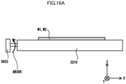
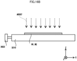
- the activation treatment device 3002 by turning over the stage 3210 as illustrated by an arrow AR306 in FIG. 16A , brings the substrate W1 or W2 into such an attitude that the bonding surface of the substrate W1 or W2 faces vertically upward. Then, the activation treatment device 3002 irradiates the bonding surface of the substrate W1 or W2 with nitrogen radicals, as illustrated by arrows AR307 in FIG. 16B .
- each of the bonding surfaces of the substrates W1 and W2 is a so-called hybrid bonding surface that includes, for example, a region that is formed of Cu and serves as an electrode and a region that is formed of an oxide film and serves as an insulating layer
- performing conventional RIE treatment with plasma causes a sheath region to be formed in a vicinity of the bonding surface of the substrate W1 or W2 and all ionized substances to be drawn in and attack the bonding surface of the substrate W1 or W2.
- Cu ions or Cu particles generated by the region formed of Cu being etched adhere to the region formed of an oxide film on the bonding surface of the substrate W1 or W2, bonding strength in the region formed of an oxide film deteriorates.
- the present configuration is suitable for activation treatment of the substrates W1 and W2 having so-called hybrid bonding surfaces.
- the RIE treatment with plasma causes resin of which the adhesive sheet is made to adhere to the bonding surfaces of the chips.
- the present configuration enables excellent activation treatment to be performed without resin of which an adhesive sheet is made adhering to the bonding surfaces of chips.
- an activation treatment device 4002 includes a stage 210, a chamber 4212, a trap plate 4214, a waveguide 4215, a magnetron 4216, and a bias applier 217. Note that, in FIG. 17 , the same reference signs as those in FIG. 2 are assigned to the same constituent components as those in activation treatment device 2 according to the embodiment.
- the activation treatment device 4002 also includes a nitrogen gas feeder 220A and an oxygen gas feeder 220B.
- the nitrogen gas feeder 220A includes a nitrogen gas storage 221A, a feeding valve 222A, and a feeding pipe 223A.
- the oxygen gas feeder 220B includes an oxygen gas storage 221B, a feeding valve 222B, and a feeding pipe 223B.
- a substrate W1 or W2 is placed on the stage 210.
- the chamber 4212 is connected to the waveguide 4215 via a glass window 4213.
- the chamber 4212 is connected to a vacuum pump 201 via an exhaust pipe 202A and an exhaust valve 203A.
- the trap plate 4214 is formed of, for example, a metal, a graphite, or the like and is maintained at a ground potential.
- a microwave generated by the magnetron 4216 is fed into the chamber 4212 through the waveguide 4215.
- the magnetron 4216 for example, a magnetron that generates a microwave having a frequency of 2.45 GHz can be employed.
- N 2 () gas has been fed into the plasma chamber 4212
- plasma PLM is formed in a vicinity of the glass window 4213 in the chamber 4212 by the microwave.
- the trap plate 4214 traps ions contained in the plasma PLM and allows only radicals to flow down to the stage 210.
- the magnetron 4216, the nitrogen gas feeder 220A, and the trap plate 4214 constitute a plasma generation source that generates the plasma PLM in the chamber 4212 and feeds N 2 () radicals in the plasma to the bonding surface of the substrate W1 or W2 supported by the stage 210.
- RIE treatment physical etching treatment
- the activation treatment device 4002 subjects the substrate W1 or W2 on the stage 210 to chemical treatment by generating ions or radicals in high density in an upper portion of the chamber 4212 by a microwave fed into the upper portion of the chamber 4212 and, when the generated ions and radicals pass through the trap plate 4214 maintained at the ground potential, trapping ions and allowing only radicals including neutral molecules to flow down to the stage 210 side of the chamber 4212.
- the activation treatment device 2 applies bias voltage to the stage 210 by the bias applier 217 while feeding nitrogen gas and oxygen gas from the upper portion of the chamber 212 at the time of the RIE treatment and stops the bias application to the stage at the time of the radical treatment was described.
- the present disclosure is not limited to the configuration, and the activation treatment device 2 may be an activation treatment device in which, for example, a trap plate (not illustrated) is arranged between the stage 210 and a region inside the plasma chamber 213. In this configuration, the trap plate is maintained at the ground potential.
- the activation treatment device 2 since, at the time of the radical treatment, ions are trapped in ICP plasma by an electric field formed in the plasma chamber 213 by the induction coil 215, it is possible to allow only radicals to flow down to the stage 210 side even without the trap plate. However, all ions are not trapped in the ICP plasma, and a certain number of ions fall to the stage 210 side. In contrast, in the activation treatment device according to the present variation, since ions are trapped by the trap plate in the radical treatment, it is possible to prevent ions from being radiated to the stage 210 side.
- the present disclosure is not limited to the example, and it may be configured such that, at the time of the RIE treatment, the trap plate is put into a floating state instead of being maintained at the ground potential and, only at the time of the radical treatment, the trap plate is maintained at the ground potential.
- ions in the plasma PLM generated in the plasma chamber 213 are not trapped by the trap plate and fall to the stage 210 side at the time of the RIE treatment and are trapped by the trap plate only at the time of the radical treatment.
- radicals ride on flows of nitrogen gas and oxygen gas and are radiated to the stage 210 at the time of the radical treatment.
- the radical treatment ions in the plasma PLM generated in the plasma chamber 213 are drawn in to the trap plate and at the same time accelerated, when passing through holes of the trap plate, are supplied with electrons by the trap plate and neutralized, and are subsequently radiated to the substrate W1 or W2 placed on the stage 210.
- it may be configured to, for example, maintain the stage 210 at the ground potential without applying a bias and maintain the trap plate in a floating state.
- ions in the plasma PLM generated in the plasma chamber 213 directly pass through the holes of the trap plate and, while being accelerated to the stage 210 side, are radiated to the substrate W1 or W2 placed on the stage 210.
- treatment similar to the RIE treatment is to be performed.
- the trap plate is maintained at the ground potential, ions are trapped by the trap plate and only radicals pass through the trap plate and are radiated to the substrate W1 or W2 placed on the stage 210.
- the afore-described configuration in which, at the time of the RIE treatment, the trap plate is put into a floating state instead of being maintained at the ground potential and, only at the time of the radical treatment, the trap plate is maintained at the ground potential or the afore-described configuration that maintains the stage 210 at the ground potential without applying a bias and maintains the trap plate in a floating state is not limited to application to the activation treatment device using so-called ICP plasma and may be applied to the activation treatment device using a microwave that was described using FIG. 17 or an activation treatment device of parallel flat plate type. In this case, it is possible to achieve a more inexpensive configuration.
- examples of the activation treatment device of parallel flat plate type include an activation treatment device 6002, as illustrated in, for example, FIG. 18 , that includes an electrode 6215 arranged in a plasma chamber 213, a bias applier 6216 to apply a bias to the electrode 6215, and a trap plate 5214.
- ions in plasma are also trapped in an electric field in a sheath region in a similar manner to ICP plasma.
- the frequency of a bias is 13.56 MHz in the RIE treatment
- use of a bias with a frequency of 27 MHz or use of a 2 GHz microwave as in the activation treatment device of parallel flat plate type or the activation treatment device using ICP plasma enables a larger number of radicals to be generated and is more effective.
- ions in the plasma PLM are trapped in a sheath region formed in the plasma chamber 213 or an electric field formed by the induction coil 215 and do not fall to the stage 210 side.
- ions in the plasma PLM are drawn in to the trap plate and accelerated, when passing through holes of the trap plate, receive electrons from the trap plate, and, while being kept accelerated as neutral molecules, are radiated to the substrate W1 or W2 placed on the stage 210.
- three methods namely a method of first performing the strongest physical treatment (1) and next performing the chemical treatment (4), a method of first performing the weak physical treatment (2) and next performing the chemical treatment (4), and a method of first performing the weak physical treatment (5) that causes a small damage to the substrate W1 or W2 and next performing the chemical treatment (4), are conceivable, and it becomes possible to select one of the three methods and perform the selected one.
- the configuration is not limited to a configuration in which the trap plate or the stage 210 is maintained at the ground potential, and bias voltage may be applied to the trap plate or the stage 210. Because of this configuration, ions passing through the trap plate are further accelerated and energy of the ions can be increased.
- the method of activation treatment is not limited to this method as long as both of bonding surfaces of the two substrates W1 and W2 are subjected to the activation treatment.
- it may be configured such that only one of the two substrates W1 and W2 is subjected to the N 2 RIE treatment and the N 2 radical treatment and the other is not subjected to at least one of the N 2 RIE treatment and the N 2 radical treatment.
- the substrate bonding device 1 applies pressure to the substrates W1 and W2 and also subjects the substrates W1 and W2 to heat treatment with the entire bonding surfaces of the substrates W1 and W2 in contact with each other was described.
- the present disclosure is not limited to the example, and it may be configured such that the substrate bonding device 1 only applies pressure to the substrates W1 and W2 with the entire bonding surfaces of the substrates W1 and W2 in contact with each other and does not perform heat treatment.
- it may be configured such that the substrate bonding device 1 only subjects the substrates W1 and W2 to heat treatment with the entire bonding surfaces of the substrates W1 and W2 in contact with each other and does not apply pressure to the substrates W1 and W2.
- the substrates W1 and W2 may be subjected to application of pressure and heat treatment in a device different from the substrate bonding device 1.
- the substrate bonding device 1 may perform processing until the temporary bonding of the substrates W1 and W2 and the heat treatment may be subsequently performed in another heating device (not illustrated).
- the present disclosure is not limited to the configuration, and it may be configured such that the substrates W1 and W2 are bonded to each other under atmospheric pressure, and, alternatively, it may be configured such that the substrates W1 and W2 are bonded to each other under an atmosphere filled with an arbitrary gas.
- the present disclosure is not limited to the configuration, and it may be configured such that no cooling device is disposed in the load lock chamber 83.
- the activation treatment device 3002 includes the particle beam source 3061
- the present disclosure is not limited to the example, and it may be configured such that the turnover device 4 includes a particle beam source.
- CMOS complementary MOS
- MEMS micro electro mechanical systems
Landscapes
- Engineering & Computer Science (AREA)
- Physics & Mathematics (AREA)
- Fluid Mechanics (AREA)
- Mechanical Engineering (AREA)
- Condensed Matter Physics & Semiconductors (AREA)
- General Physics & Mathematics (AREA)
- Manufacturing & Machinery (AREA)
- Computer Hardware Design (AREA)
- Microelectronics & Electronic Packaging (AREA)
- Power Engineering (AREA)
- Pressure Welding/Diffusion-Bonding (AREA)
- Combinations Of Printed Boards (AREA)
Applications Claiming Priority (2)
| Application Number | Priority Date | Filing Date | Title |
|---|---|---|---|
| JP2020164962 | 2020-09-30 | ||
| PCT/JP2021/033291 WO2022070835A1 (ja) | 2020-09-30 | 2021-09-10 | 基板接合方法および基板接合システム |
Publications (1)
| Publication Number | Publication Date |
|---|---|
| EP4224512A1 true EP4224512A1 (en) | 2023-08-09 |
Family
ID=80950377
Family Applications (1)
| Application Number | Title | Priority Date | Filing Date |
|---|---|---|---|
| EP21875137.8A Withdrawn EP4224512A1 (en) | 2020-09-30 | 2021-09-10 | Substrate bonding method and substrate bonding system |
Country Status (5)
| Country | Link |
|---|---|
| US (1) | US12409644B2 (enExample) |
| EP (1) | EP4224512A1 (enExample) |
| JP (2) | JP7440047B2 (enExample) |
| TW (1) | TW202230457A (enExample) |
| WO (1) | WO2022070835A1 (enExample) |
Families Citing this family (2)
| Publication number | Priority date | Publication date | Assignee | Title |
|---|---|---|---|---|
| CN209933070U (zh) | 2018-01-07 | 2020-01-14 | 苏州杰成医疗科技有限公司 | 心脏瓣膜假体 |
| JP2025144080A (ja) * | 2024-03-19 | 2025-10-02 | 株式会社Screenホールディングス | 基板接合方法および基板接合装置 |
Family Cites Families (16)
| Publication number | Priority date | Publication date | Assignee | Title |
|---|---|---|---|---|
| JP2888258B2 (ja) | 1990-11-30 | 1999-05-10 | 東京エレクトロン株式会社 | 基板処理装置および基板処理方法 |
| JP2701709B2 (ja) * | 1993-02-16 | 1998-01-21 | 株式会社デンソー | 2つの材料の直接接合方法及び材料直接接合装置 |
| US6780759B2 (en) * | 2001-05-09 | 2004-08-24 | Silicon Genesis Corporation | Method for multi-frequency bonding |
| JP3980539B2 (ja) | 2003-08-29 | 2007-09-26 | 唯知 須賀 | 基板接合方法、照射方法、および基板接合装置 |
| JP3790995B2 (ja) | 2004-01-22 | 2006-06-28 | 有限会社ボンドテック | 接合方法及びこの方法により作成されるデバイス並びに接合装置 |
| JP2006080314A (ja) * | 2004-09-09 | 2006-03-23 | Canon Inc | 結合基板の製造方法 |
| JP2006339363A (ja) * | 2005-06-01 | 2006-12-14 | Bondtech Inc | 表面活性化方法および表面活性化装置 |
| JP4671900B2 (ja) * | 2006-04-06 | 2011-04-20 | パナソニック株式会社 | 接合方法および接合装置 |
| JP2008202114A (ja) | 2007-02-21 | 2008-09-04 | Canon Anelva Corp | 薄膜作成装置 |
| JP4967842B2 (ja) | 2007-06-18 | 2012-07-04 | セイコーエプソン株式会社 | シリコン基材の接合方法、液滴吐出ヘッド、液滴吐出装置および電子デバイス |
| JP5282392B2 (ja) | 2007-11-05 | 2013-09-04 | セイコーエプソン株式会社 | 直接接合用ウェハ |
| IN2015DN03311A (enExample) * | 2012-09-28 | 2015-10-09 | Dainippon Printing Co Ltd | |
| JP6395333B2 (ja) | 2014-04-25 | 2018-09-26 | 須賀 唯知 | 基板接合装置および基板接合方法 |
| US11837444B2 (en) | 2016-11-07 | 2023-12-05 | Tadatomo Suga | Substrate joining method, substrate joining system and method for controlling hydrophilic treatment device |
| US20210265300A1 (en) | 2018-08-31 | 2021-08-26 | Bondtech Co., Ltd. | Bonding system and bonding method |
| JP6967032B2 (ja) | 2019-03-29 | 2021-11-17 | Jx金属株式会社 | 電解装置及び電解方法 |
-
2021
- 2021-09-10 JP JP2022553755A patent/JP7440047B2/ja active Active
- 2021-09-10 WO PCT/JP2021/033291 patent/WO2022070835A1/ja not_active Ceased
- 2021-09-10 US US18/245,895 patent/US12409644B2/en active Active
- 2021-09-10 EP EP21875137.8A patent/EP4224512A1/en not_active Withdrawn
- 2021-09-14 TW TW110134185A patent/TW202230457A/zh unknown
-
2023
- 2023-11-15 JP JP2023194100A patent/JP2024009082A/ja active Pending
Also Published As
| Publication number | Publication date |
|---|---|
| JP7440047B2 (ja) | 2024-02-28 |
| WO2022070835A1 (ja) | 2022-04-07 |
| US12409644B2 (en) | 2025-09-09 |
| JP2024009082A (ja) | 2024-01-19 |
| US20240009984A1 (en) | 2024-01-11 |
| TW202230457A (zh) | 2022-08-01 |
| JPWO2022070835A1 (enExample) | 2022-04-07 |
Similar Documents
| Publication | Publication Date | Title |
|---|---|---|
| JP6617227B2 (ja) | 基板接合装置および基板接合方法 | |
| JP4133333B2 (ja) | 被処理体の処理方法及びその処理装置 | |
| JP6388272B1 (ja) | 基板接合方法、基板接合システムおよび親水化処理装置の制御方法 | |
| EP4224512A1 (en) | Substrate bonding method and substrate bonding system | |
| JP6429179B2 (ja) | 基板接合装置および基板接合方法 | |
| JP6994210B2 (ja) | 接合システムおよび接合方法 | |
| US20090258159A1 (en) | Novel treatment for mask surface chemical reduction | |
| JP2019204832A (ja) | 部品実装システム、基板接合システム、部品実装方法および基板接合方法 | |
| KR20190109239A (ko) | 플라스마 처리 방법 및 플라스마 처리 장치 | |
| JP2006339363A (ja) | 表面活性化方法および表面活性化装置 | |
| EP3367425A1 (en) | A method for direct bonding of semiconductor substrates | |
| JP2002509852A (ja) | ガラス表面の水蒸気プラズマ処理 | |
| JP3423186B2 (ja) | 処理方法 | |
| JP2024056041A (ja) | 接合方法 | |
| JP6142305B2 (ja) | 静電吸着方法及び静電吸着装置 | |
| US7261780B2 (en) | Ceramic susceptor and a method of cleaning the same | |
| JP6067210B2 (ja) | プラズマ処理装置 | |
| WO2022158520A1 (ja) | 接合方法、接合装置および接合システム | |
| US7811898B2 (en) | Method and device for bonding wafers | |
| JP6174210B2 (ja) | 載置台およびプラズマ処理装置 | |
| JP2025087176A (ja) | 接合方法、構造体および接合システム | |
| JP6366307B2 (ja) | 洗浄システム、および洗浄方法 | |
| CN117121158A (zh) | 接合方法、接合装置及接合系统 |
Legal Events
| Date | Code | Title | Description |
|---|---|---|---|
| STAA | Information on the status of an ep patent application or granted ep patent |
Free format text: STATUS: THE INTERNATIONAL PUBLICATION HAS BEEN MADE |
|
| PUAI | Public reference made under article 153(3) epc to a published international application that has entered the european phase |
Free format text: ORIGINAL CODE: 0009012 |
|
| STAA | Information on the status of an ep patent application or granted ep patent |
Free format text: STATUS: REQUEST FOR EXAMINATION WAS MADE |
|
| 17P | Request for examination filed |
Effective date: 20230424 |
|
| AK | Designated contracting states |
Kind code of ref document: A1 Designated state(s): AL AT BE BG CH CY CZ DE DK EE ES FI FR GB GR HR HU IE IS IT LI LT LU LV MC MK MT NL NO PL PT RO RS SE SI SK SM TR |
|
| DAV | Request for validation of the european patent (deleted) | ||
| DAX | Request for extension of the european patent (deleted) | ||
| STAA | Information on the status of an ep patent application or granted ep patent |
Free format text: STATUS: THE APPLICATION HAS BEEN WITHDRAWN |
|
| 18W | Application withdrawn |
Effective date: 20240926 |