WO2022070835A1 - 基板接合方法および基板接合システム - Google Patents
基板接合方法および基板接合システム Download PDFInfo
- Publication number
- WO2022070835A1 WO2022070835A1 PCT/JP2021/033291 JP2021033291W WO2022070835A1 WO 2022070835 A1 WO2022070835 A1 WO 2022070835A1 JP 2021033291 W JP2021033291 W JP 2021033291W WO 2022070835 A1 WO2022070835 A1 WO 2022070835A1
- Authority
- WO
- WIPO (PCT)
- Prior art keywords
- substrates
- substrate
- bonding
- chamber
- treatment
- Prior art date
- Legal status (The legal status is an assumption and is not a legal conclusion. Google has not performed a legal analysis and makes no representation as to the accuracy of the status listed.)
- Ceased
Links
Images


Classifications
-
- H—ELECTRICITY
- H01—ELECTRIC ELEMENTS
- H01L—SEMICONDUCTOR DEVICES NOT COVERED BY CLASS H10
- H01L21/00—Processes or apparatus adapted for the manufacture or treatment of semiconductor or solid state devices or of parts thereof
- H01L21/02—Manufacture or treatment of semiconductor devices or of parts thereof
-
- B—PERFORMING OPERATIONS; TRANSPORTING
- B32—LAYERED PRODUCTS
- B32B—LAYERED PRODUCTS, i.e. PRODUCTS BUILT-UP OF STRATA OF FLAT OR NON-FLAT, e.g. CELLULAR OR HONEYCOMB, FORM
- B32B37/00—Methods or apparatus for laminating, e.g. by curing or by ultrasonic bonding
- B32B37/12—Methods or apparatus for laminating, e.g. by curing or by ultrasonic bonding characterised by using adhesives
-
- B—PERFORMING OPERATIONS; TRANSPORTING
- B32—LAYERED PRODUCTS
- B32B—LAYERED PRODUCTS, i.e. PRODUCTS BUILT-UP OF STRATA OF FLAT OR NON-FLAT, e.g. CELLULAR OR HONEYCOMB, FORM
- B32B37/00—Methods or apparatus for laminating, e.g. by curing or by ultrasonic bonding
- B32B37/10—Methods or apparatus for laminating, e.g. by curing or by ultrasonic bonding characterised by the pressing technique, e.g. using action of vacuum or fluid pressure
-
- B—PERFORMING OPERATIONS; TRANSPORTING
- B32—LAYERED PRODUCTS
- B32B—LAYERED PRODUCTS, i.e. PRODUCTS BUILT-UP OF STRATA OF FLAT OR NON-FLAT, e.g. CELLULAR OR HONEYCOMB, FORM
- B32B38/00—Ancillary operations in connection with laminating processes
- B32B38/10—Removing layers, or parts of layers, mechanically or chemically
-
- B—PERFORMING OPERATIONS; TRANSPORTING
- B32—LAYERED PRODUCTS
- B32B—LAYERED PRODUCTS, i.e. PRODUCTS BUILT-UP OF STRATA OF FLAT OR NON-FLAT, e.g. CELLULAR OR HONEYCOMB, FORM
- B32B2309/00—Parameters for the laminating or treatment process; Apparatus details
- B32B2309/04—Time
-
- B—PERFORMING OPERATIONS; TRANSPORTING
- B32—LAYERED PRODUCTS
- B32B—LAYERED PRODUCTS, i.e. PRODUCTS BUILT-UP OF STRATA OF FLAT OR NON-FLAT, e.g. CELLULAR OR HONEYCOMB, FORM
- B32B2309/00—Parameters for the laminating or treatment process; Apparatus details
- B32B2309/12—Pressure
-
- B—PERFORMING OPERATIONS; TRANSPORTING
- B32—LAYERED PRODUCTS
- B32B—LAYERED PRODUCTS, i.e. PRODUCTS BUILT-UP OF STRATA OF FLAT OR NON-FLAT, e.g. CELLULAR OR HONEYCOMB, FORM
- B32B2310/00—Treatment by energy or chemical effects
- B32B2310/08—Treatment by energy or chemical effects by wave energy or particle radiation
- B32B2310/0875—Treatment by energy or chemical effects by wave energy or particle radiation using particle radiation
- B32B2310/0881—Treatment by energy or chemical effects by wave energy or particle radiation using particle radiation using ion-radiation, e.g. alpha-rays
-
- B—PERFORMING OPERATIONS; TRANSPORTING
- B32—LAYERED PRODUCTS
- B32B—LAYERED PRODUCTS, i.e. PRODUCTS BUILT-UP OF STRATA OF FLAT OR NON-FLAT, e.g. CELLULAR OR HONEYCOMB, FORM
- B32B2310/00—Treatment by energy or chemical effects
- B32B2310/14—Corona, ionisation, electrical discharge, plasma treatment
Definitions
- the present invention relates to a substrate bonding method and a substrate bonding system.
- the substrates are bonded together with water molecules intervening in the atmosphere, so that even if sufficient OH groups are not formed on the bonding surface of the original substrate, the bonding surface of the substrate is formed.
- the water molecules intervening in the group changed to OH groups and could be changed to strong covalent bonds by heating.
- a joining method such as bonding the boards together while bending the central portion of the boards.
- problems such as distortion of the substrate and deterioration of the alignment accuracy between the substrates.
- the method of joining the substrates in a vacuum is an effective method for obtaining good bonding between the substrates.
- a substrate bonding method for bonding two substrates has been proposed by using reactive ion etching and radical irradiation on the bonding surface of the two substrates to be bonded in combination (for example). See Patent Document 1).
- hydroxyl groups OH groups
- OH groups hydroxyl groups
- the bonding surfaces of the two substrates to be bonded are exposed to oxygen plasma to perform reactive ion etching, and then the bonding surfaces of the two substrates are irradiated with nitrogen radicals. After that, the two substrates are joined by contacting the joining surfaces of the two substrates and applying pressure.
- the amount of OH groups generated on the bonding surface of the two substrates may be insufficient, and the bonding strength of the two bonded substrates may not be sufficient. Therefore, there is a demand for a substrate bonding method capable of more firmly bonding two substrates to each other by generating a sufficient amount of OH groups on the bonding surface of the two substrates.
- the present invention has been made in view of the above reasons, and an object of the present invention is to provide a substrate bonding method and a substrate bonding system capable of firmly bonding two substrates.
- the substrate bonding method is: A substrate bonding method for joining two substrates.
- a gas exposure step of exposing the joint surface of the two substrates to a gas containing water within a preset reference time, and a gas exposure step is included.
- the wafer bonding system according to the present invention from another point of view is A wafer bonding system that joins two boards.
- An activation treatment for activating the joint surface by performing at least one of an etching treatment using nitrogen gas and irradiation with a nitrogen radical is performed on at least one of the joint surfaces of each of the two substrates to be joined to each other. Then, within a preset reference time, the activation treatment apparatus that exposes the joint surface of the two substrates to a gas containing water, and A substrate bonding device for joining the two substrates whose bonding surface has been activated by the activation processing device is provided.
- At least one of the bonding surfaces of the two substrates to be bonded to each other is subjected to at least one of reactive ion etching using nitrogen gas and irradiation of nitrogen radicals.
- nitrogen gas and irradiation of nitrogen radicals To activate.
- a state in which nitrogen is adsorbed on the surface or oxynitride is formed is formed on the surface of the substrate.
- This N active state reacts with water to form OH groups and contributes to an increase in bond strength.
- the N active state formed on the joint surface of the substrate is unstable, and the active state is inactivated as it is. As a result, the joint strength cannot be maintained.
- the joint surface of the substrate after activating the joint surface of the substrate, it is necessary to bring it into contact with water molecules within a preset reference time. Therefore, in the present invention, after activating the joint surface of the substrate, the joint surface of the substrate is exposed to a gas containing water within a preset reference time. As a result, since the joint surface of the substrate can be brought into contact with water molecules in an N-active state, many oxynitrides can be formed on the joint surface of the substrate. Then, when the bonding surfaces of the two substrates are brought into contact with each other to temporarily bond the two substrates and then heat treatment is performed, many oxynitrides existing between the bonding surfaces of the two substrates are replaced with OH groups. This makes it possible to form a relatively large number of hydrogen bonds.
- (A-1) is a schematic diagram showing a state in which water molecules are attached to the substrate
- (A-2) is a schematic diagram showing a state in which the substrates are in contact with each other under atmospheric pressure
- (A-). 3) is a schematic diagram showing the transition of the state of the substrate when the heat treatment is performed under atmospheric pressure
- (B-1) is a schematic diagram showing the state in which water molecules are attached to the substrate
- -2) is a schematic diagram showing the transition of the state of the substrates when the substrates are brought close to each other under reduced pressure
- (B-3) is a schematic diagram showing the state of bringing the substrates into contact with each other under reduced pressure.
- (C-1) are schematic views showing the state of the substrate after the activation treatment step according to the present embodiment
- (C-2) is the state of the substrate in the joining step according to the present embodiment.
- (C-3) is a schematic diagram which shows the state which the substrates were in contact with each other in the joining process which concerns on this embodiment.
- the bonding surfaces of the two substrates are activated in a chamber under reduced pressure, and then the substrates are brought into contact with each other to pressurize and heat the two substrates. It is a system to join.
- the activation treatment at least one of the bonding surfaces of the two substrates bonded to each other is subjected to at least one of reactive ion etching using nitrogen gas and irradiation of nitrogen radicals to prepare the bonding surfaces of the substrates. Activate.
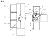
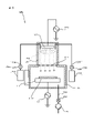
- the wafer bonding system includes introduction ports 811, 812, take-out ports 813, a first transfer device 82, a cleaning device 3, a reversing device 4, and an activation process.
- a device 2, a substrate bonding device 1, a second transfer device 84, a control unit 9, and a load lock chamber 83 are provided.
- the control unit 9 controls the first transfer device 82, the cleaning device 3, the reversing device 4, the activation processing device 2, the substrate bonding device 1, and the second transfer device 84.
- the first transport device 82, the second transport device 84, and the cleaning device 3 are provided with a HEPA (High Efficiency Particulate Air) filter (not shown).
- HEPA High Efficiency Particulate Air
- the first transfer device 82 includes a transfer robot 821 having an arm provided with a holding portion for holding the substrate at the tip portion.
- the transfer robot 821 can move along the alignment direction of the introduction ports 811 and 812 and the take-out port 813, and can change the direction of the tip of the arm by turning.
- the second transfer device 84 also includes a transfer robot 841 having an arm provided with a holding portion for holding the substrate at the tip end portion.
- the transfer robot 841 can change the direction of the tip of the arm by turning.
- the holding portion has a vacuum chuck, an electrostatic chuck, etc., and sucks and holds the side of the substrate opposite to the joint surface side.
- the load lock chamber 83 is provided with a cooling device (not shown) for cooling a stage (not shown) that supports the substrates W1 and W2. Then, for example, when the humidity in the load lock chamber 83 is set to 50% when the temperature is 25 ° C., the cooling device cools the stage to 18 ° C., so that the substrate mounted on the stage is placed on the stage. Humidity near W1 and W2 is set to about 80%.
- the cleaning device 3 cleans while discharging liquids such as water and cleaning liquid toward the conveyed substrate.
- the cleaning device includes a stage that supports the substrate (not shown), an XY direction drive unit (not shown) that drives the stage in two directions (XY directions) that are orthogonal to each other in the vertical direction and orthogonal to each other, and ultrasonic waves or It has a cleaning head (not shown) that discharges water or cleaning liquid that has been subjected to megasonic vibration. Further, the cleaning device 3 has a rotation driving unit (not shown) that rotates the stage in a plane orthogonal to the vertical direction.
- the cleaning device 3 cleans the entire surface of the joint surface of the substrate by scanning the stage in the XY direction while spraying water to which ultrasonic waves are applied by the cleaning head onto the joint surface of the substrate. Then, the cleaning device 3 stops the discharge of water by the cleaning head, and then spin-drys the substrate by rotating the stage.
- the reversing device 4 has a substrate holding unit (not shown) that receives and holds the substrate from the tip of the arm of the transfer robot 841, and a driving unit (not shown) that inverts the substrate holding portion while the substrate holding unit holds the substrate. Not shown) and.
- the substrate holding portion has, for example, a vacuum chuck, an electrostatic chuck, or the like that holds the side opposite to the joint surface side of the substrate.
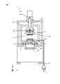
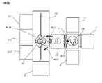
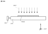
- the activation treatment apparatus 2 performs activation treatment on the joint surface of the substrate by performing at least one of reactive ion etching using nitrogen gas and irradiation with nitrogen radicals to activate the joint surface. An activation process is performed to activate the joint surface of the substrate.
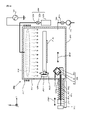
- the activation processing device 2 is a device that generates inductively coupled plasma (ICP), and as shown in FIG. 2, the stage 210, the chamber 212, the plasma chamber 213, and the outside of the plasma chamber 213. It has a wound inductive coil 215 and a high frequency power supply 216 that supplies a high frequency current to the inductive coil 215.
- the plasma chamber 213 is made of, for example, quartz glass.
- the activation treatment device 2 has a nitrogen gas supply unit 220A and an oxygen gas supply unit 220B.
- the nitrogen gas supply unit 220A includes a nitrogen gas storage unit 221A, a supply valve 222A, a supply pipe 223A, and a bias application unit 217.
- the oxygen gas supply unit 220B includes an oxygen gas storage unit 221B, a supply valve 222B, and a supply pipe 223B.
- the substrates W1 and W2 are placed on the stage 210.
- the chamber 212 communicates with the plasma chamber 213.
- the chamber 212 is connected to the vacuum pump 201 via an exhaust pipe 202A and an exhaust valve 203A. When the vacuum pump 201 is operated with the exhaust valve 203A opened, the gas in the chamber 212 is discharged to the outside of the chamber 212 through the exhaust pipe 202A, and the air pressure in the chamber 212 is reduced (decompressed).
- the high frequency power supply 216 one that supplies a high frequency current of, for example, 27 MHz to the induction coil 215 can be adopted. Then, when a high-frequency current is supplied to the induction coil 215 with the N 2 gas introduced into the plasma chamber 213, a plasma PLM is formed in the plasma chamber 213.
- the induction coil 215 traps the ions contained in the plasma in the plasma chamber 213, the configuration may be such that there is no trap plate in the portion between the plasma chamber 213 and the chamber 212.
- plasma PLM is generated in the plasma chamber 213 and N2 radicals in the plasma are supplied to the junction surface of the substrates W1 and W2 supported by the stage 210.
- the plasma source is configured.
- a device for generating an ICP including an inductive coil 215 and a high frequency power supply 216 as the activation processing device 2 has been described, but the present invention is not limited to this, and a plasma chamber is used instead. It includes a flat plate electrode arranged outside the 213, a high frequency power source electrically connected to the flat plate electrode, and a trap plate arranged in a portion between the plasma chamber 213 and the chamber 212 to trap ions in the plasma.
- It may be a device that generates capacitively coupled plasma (CCP).
- CCP capacitively coupled plasma
- the high frequency power supply for example, one to which a high frequency bias of 27 MHz is applied can be adopted.
- the electric power supplied from the high frequency power source into the plasma chamber is set to, for example, 250 W.
- the bias application unit 217 is a high frequency power supply that applies a high frequency bias to the substrates W1 and W2 supported by the stage 210.
- the bias application unit 217 for example, one that generates a high frequency bias of 13.56 MHz can be adopted.
- a sheath region in which ions having kinetic energy repeatedly collide with the substrates W1 and W2 is generated in the vicinity of the junction surface of the substrates W1 and W2. do.
- the joint surfaces of the substrates W1 and W2 are etched by the ions having kinetic energy existing in this sheath region.
- the activation treatment apparatus 2 exposes the joint surfaces of the substrates W1 and W2 to a gas containing water within a preset reference time after performing the above-mentioned activation treatment.
- the gas containing water include the atmosphere and water gas.
- An introduction pipe (not shown) for introducing air or water gas into the chamber 212 is connected to the chamber 212, and an introduction valve (not shown) is inserted in the introduction pipe.
- the activation processing device 2 introduces air or water gas into the chamber 212 by closing the exhaust valve 203A and opening the introduction valve, thereby making the joint surface of the substrates W1 and W2 air or water. Expose to gas.
- a water gas supply unit (not shown) for supplying water gas is connected to the introduction pipe.
- the water gas supply unit generates and supplies water gas by mixing carrier gas such as argon (Ar), nitrogen (N2 ()), helium (He), and oxygen (O2 ()) with vaporized water. It should be done.
- carrier gas such as argon (Ar), nitrogen (N2 ()), helium (He), and oxygen (O2 ()
- nitrogen is used as a carrier gas, and a mixture of 50% vaporized water is adopted as the water gas.
- the substrate bonding device 1 joins the substrates W1 and W2 activated in the activation processing device 2 to each other.
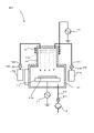
- the substrate bonding device 1 includes a chamber 120, a stage 141, a head 142, a stage drive unit 143, a head drive unit 144, a substrate heating unit 1411, 1421, and a misalignment amount measuring unit. 150 and.
- the ⁇ Z direction of FIG. 3 will be described as the vertical direction and the XY direction will be described as the horizontal direction.
- the chamber 120 is connected to the vacuum pump 121 via an exhaust pipe 122B and an exhaust valve 123B.
- the vacuum pump 121 When the vacuum pump 121 is operated with the exhaust valve 123B opened, the gas in the chamber 120 is discharged to the outside of the chamber 120 through the exhaust pipe 122B, and the air pressure in the chamber 120 is reduced (decompressed). Further, the air pressure (vacuum degree) in the chamber 120 can be adjusted by adjusting the exhaust amount by varying the opening / closing amount of the exhaust valve 123B. Further, an air introduction pipe (not shown) is connected to the chamber 120, and an air introduction valve (not shown) is inserted in the air introduction pipe. Then, the wafer bonding device 1 closes the exhaust valve 123B and opens the air introduction valve to bring the air pressure in the chamber 120 to atmospheric pressure.
- the stage 141 and the head 142 are arranged in the chamber 120 so as to face each other in the Z direction.
- the stage 141 supports the substrate W1 on its upper surface
- the head 142 supports the substrate W2 on its lower surface.
- the upper surface of the stage 141 and the lower surface of the head 142 are roughened in consideration of the case where the contact surfaces of the substrates W1 and W2 with the stage 141 and the head 142 are mirror surfaces and are not easily peeled off from the stage 141 and the head 142. It may have been done.
- the stage 141 and the head 142 have holding mechanisms (not shown) for holding the substrates W1 and W2, respectively.
- the holding mechanism includes an electrostatic chuck, a vacuum chuck, and the like.
- the stage drive unit 143 can move the stage 141 in the XY direction or rotate it around the Z axis.
- the head drive unit 144 raises and lowers the head 142 in the vertical direction (see arrow AR1 in FIG. 3).
- the head drive unit 144 brings the head 142 closer to the stage 141 by moving the head 142 downward. Further, the head drive unit 144 moves the head 142 upward to move the head 142 away from the stage 141. Then, when the head driving unit 144 exerts a driving force on the head 142 in a direction approaching the stage 141 in a state where the substrates W1 and W2 are in contact with each other, the substrate W2 is pressed against the substrate W1.
- the head drive unit 144 is provided with a pressure sensor 148 for measuring the driving force that the head drive unit 144 exerts on the head 142 in the direction approaching the stage 141.
- the pressure sensor 148 is, for example, a load cell, and from this measured value, the pressure acting on the joint surface of the substrates W1 and W2 when the substrate W2 is pressed against the substrate W1 by the head drive unit 144 can be detected.
- the substrate heating units 1411 and 1421 are composed of, for example, an electric heater.
- the substrate heating units 1411, 1421 heat the substrates W1 and W2 by transferring heat to the substrates W1 and W2 supported by the stage 141 and the head 142. Further, by adjusting the calorific value of the substrate heating portions 1411, 1421, the temperature of the substrates W1, W2 or their joint surfaces can be adjusted.
- the misalignment amount measuring unit 150 measures the amount of misalignment of the substrate W1 in the horizontal direction with respect to the substrate W2 by recognizing the positions of the alignment marks (alignment marks) provided on the substrates W1 and W2 respectively.
- the misalignment amount measuring unit 150 recognizes the alignment marks of the substrates W1 and W2 by using, for example, light transmitted through the substrates W1 and W2 (for example, infrared light).
- the stage drive unit 143 moves or rotates the stage 141 in the horizontal direction based on the amount of misalignment measured by the misalignment measurement unit 150, thereby aligning the substrates W1 and W2 with each other. (Alignment operation) is executed.
- the measurement of the misalignment amount by the misalignment amount measuring unit 150 and the alignment operation of the stage driving unit 143 are both executed under the control of the control unit 9.
- the control unit 9 is, for example, a programmable logic controller.
- the control unit 9 calculates the pressure at which the substrates W1 and W2 are pressed against each other based on the measurement signals input from the pressure sensor, the misalignment amount measuring unit 150, and the like, and the relative positions of the substrates W1 and W2. Calculate the amount of deviation. Further, the control unit 9 controls the operation of the stage drive unit 143 and the head drive unit 144 by outputting a control signal to the stage drive unit 143 and the head drive unit 144 based on the calculated pressure or the position slip amount. Further, the control unit 9 controls these operations by outputting control signals to the substrate heating units 1411, 1421, the high frequency power supply 216, the bias application unit 217, the supply valves 222A and 222B, and the transfer robots 821 and 841.
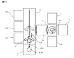
- the flow of operations from when the substrates W1 and W2 are put into the substrate bonding system until the substrates W1 and W2 are bonded and taken out from the substrate bonding system is shown in FIGS. 4A to 4A.
- the boards W1 and W2 are first arranged at the introduction ports 811 and 812 shown in FIG. 4A.
- the substrates W1 and W2 include a Si substrate, a glass substrate, an oxide substrate (for example, a silicon oxide (SiO 2 ) substrate, an alumina substrate (Al 2 O 3 ), etc.), and a nitride substrate (for example, silicon nitride (SiN)).
- At least one of the substrates W1 and W2 may have a metal portion and an insulating film exposed on the joint surface thereof. Alternatively, at least one of the substrates W1 and W2 may have an insulating film formed by depositing an oxide or a nitride on the joint surface thereof.
- the substrate W1 will be described as a glass substrate or an oxide substrate, and the substrate W2 will be described as a Si substrate or a nitride substrate.
- the introduction port 811 for example, the substrate W2 held by the head 142 in the wafer bonding apparatus 1 is arranged, and in the introduction port 812, for example, the substrate W1 mounted on the stage 141 in the wafer bonding apparatus 1 is arranged.
- the transfer robot 821 takes out the board W2 from the introduction port 811 as shown by the arrow AR11 in FIG. 4A.
- the transfer robot 821 moves to a position where the substrate W2 is carried into the load lock chamber 83 in the first transfer device 82 while holding the substrate W2.
- the transfer robot 821 takes out the substrate W1 from the introduction port 812, and then holds the substrate W1 while holding the load lock chamber 83 in the first transfer device 82. Move to the position where the board W1 is carried in.
- the transfer robot 821 is oriented so that the tip of the arm faces the load lock chamber 83 side as shown by the arrow AR13 in FIG. 4A. Turn to. Subsequently, the transfer robot 821 inserts the tip end portion of the arm into the load lock chamber 83 by extending the arm as shown by the arrow AR14 in FIG. 4B. Then, the substrates W1 and W2 are transferred from the tip end portion of the arm to the stage in the load lock chamber 83. After that, when the transfer of the substrates W1 and W2 to the stage in the load lock chamber 83 is completed, the transfer robot 821 contracts the arm as shown by the arrow AR15 in FIG. 5A. Then, the door on the first transfer device 82 side of the load lock chamber 83 is closed.
- the transport robot 841 extends the arm with the tip of the arm facing the load lock chamber 83 side. Then, when the substrates W1 and W2 are transferred from the stage to the tip of the arm in the load lock chamber 83, the transfer robot 841 is as shown by the arrow AR16 in FIG. 5A. The substrates W1 and W2 are taken out from the load lock chamber 83 by contracting the arm. After that, the door of the load lock chamber 83 on the second transport device 84 side is closed. Next, as shown by the arrow AR17 in FIG.
- the transfer robot 841 swivels so that the tip of the arm faces the activation processing device 2 side, and the activation processing device 2 moves the loading / unloading ports of the substrates W1 and W2. To open. Subsequently, the transfer robot 841 extends the arm and inserts the tip end portion of the arm into the activation processing device 2. Then, as shown by the arrow AR18 in FIG. 5B, the substrates W1 and W2 are transferred from the tip of the arm of the transfer robot 841 to the stage 210 (see FIG. 2) of the activation processing device 2. After that, the transfer robot 841 contracts the arm, and then the activation processing device 2 closes the carry-in / out ports of the substrates W1 and W2.
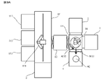
- the activation processing apparatus 2 performs at least one of reactive ion etching using nitrogen gas and irradiation of nitrogen radicals on at least one of the bonding surfaces of the substrates W1 and W2 to be bonded to each other.
- the activation treatment step of activating the joint surface is performed.
- the activation processing apparatus 2 has a different processing sequence depending on the type of substrate for which the joint surface is activated.
- the supply valve 222A shown in FIG. 2 is opened to supply the nitrogen gas storage unit 221A to the supply pipe 223A. N 2 gas is introduced into the chamber 212 through the chamber 212.
- the activation processing device 2 applies a high-frequency bias to the substrates W1 and W2 mounted on the stage 210 by the bias application unit 217 in a state where the supply of the high-frequency current from the high-frequency power supply 216 to the induction coil 215 is stopped. Apply. As a result, reactive ion etching (RIE) using N2 gas is performed on the joint surface of the substrate W1. Subsequently, the activation processing device 2 starts supplying a high frequency current from the high frequency power supply 216 to the induction coil 215 to generate plasma with N 2 gas. At this time, the activation processing device 2 stops applying the high frequency bias to the substrate W1 by the bias applying unit 217. In this way, the N2 radical is irradiated to the joint surface of the substrate W1.
- RIE reactive ion etching
- the chamber 212 is first opened from the oxygen gas storage unit 221B through the supply pipe 223B by opening the supply valve 222B. Introduce O 2 gas inside.
- the activation processing device 2 applies a high-frequency bias to the substrate W2 mounted on the stage 210 by the bias application unit 217 in a state where the supply of the high-frequency current from the high-frequency power supply 216 to the induction coil 215 is stopped. ..
- reactive ion etching (RIE) using O 2 gas is performed on the joint surface of the substrate W2.
- the activation processing device 2 exhausts the O 2 gas in the chamber 212 by closing the supply valve 222B and stopping the supply of the O 2 gas from the O 2 gas storage unit 221B into the chamber 212. After that, the activation processing device 2 introduces N2 gas from the nitrogen gas storage unit 221A into the chamber 212 through the supply pipe 223A by opening the supply valve 222A. After that, the activation processing device 2 starts supplying a high frequency current from the high frequency power supply 216 to the induction coil 215, and generates plasma with N 2 gas. At this time, the activation processing device 2 stops applying the high frequency bias to the substrate W2 by the bias applying unit 217.
- the N2 radical is irradiated to the joint surface of the substrate W2.
- the activation treatment apparatus 2 performs a gas exposure step of exposing the joint surfaces of the substrates W1 and W2 to the atmosphere or water gas within a preset reference time. Then, the activation processing device 2 opens the carry-in / out ports of the substrates W1 and W2.
- the transfer robot 841 extends the arm and inserts the tip of the arm into the activation processing device 2, and the substrates W1 and W2 are transferred from the stage 210 to the tip of the arm.
- the transfer robot 841 takes out the substrates W1 and W2 from the activation processing device 2 by contracting the arm, as shown by the arrow AR19 in FIG. 6A.
- the transfer robot 841 turns so that the tip of the arm faces the load lock chamber 83 side, the door of the load lock chamber 83 on the second transfer device 84 side opens. Will be done.
- the transfer robot 841 extends the arm and inserts the tip of the arm into the load lock chamber 83, and the substrates W1 and W2 are transferred from the tip of the arm to the stage in the load lock chamber 83.
- the transfer robot 841 contracts the arm and closes the door of the load lock chamber 83 on the second transfer device 84 side.
- the transfer robot 821 extends the arm with the tip of the arm facing the load lock chamber 83 side, and the tip of the arm is extended. The part is inserted into the load lock chamber 83. Then, the substrates W1 and W2 are transferred from the stage in the load lock chamber 83 to the tip of the arm of the transfer robot 821. After that, as shown by the arrow AR22 in FIG. 6B, the transfer robot 821 takes out the substrates W1 and W2 from the load lock chamber 83 by contracting the arm, and then the door on the first transfer device 82 side of the load lock chamber 83. Closes.
- the transfer robot 821 turns so that the tip of the arm faces the cleaning device 3 side, as shown by the arrow AR23 in FIG. 6B. Subsequently, as shown by the arrow AR24 in FIG. 7A, the transfer robot 821 moves to a position where the substrates W1 and W2 in the first transfer device 82 are carried into the cleaning device 3 while holding the substrates W1 and W2. After that, when the cleaning device 3 opens the carry-in / out ports of the substrates W1 and W2, the transfer robot 821 extends the arm and inserts the tip end portion of the arm into the cleaning device 3. Then, as shown by the arrow AR25 in FIG. 7A, the substrates W1 and W2 are transferred from the tip of the arm of the transfer robot 821 to the stage of the cleaning device 3.
- the cleaning device 3 scans the stage on which the substrates W1 and W2 are placed in the XY directions while spraying water to which ultrasonic waves are applied from the cleaning head onto the joint surfaces of the substrates W1 and W2, and the substrates W1 and W2. Clean the entire surface of the joint surface. As a result, foreign matter adhering to the joint surfaces of the substrates W1 and W2 is removed. Subsequently, the cleaning device 3 stops the discharge of water by the cleaning head, and then spin-drys the substrate by rotating the stage to complete the cleaning process. After that, the cleaning device 3 opens the carry-in / out ports of the substrates W1 and W2 when the series of cleaning processes is completed.
- the transfer robot 821 extends the arm and inserts the tip of the arm into the cleaning device 3, and the substrates W1 and W2 are transferred from the stage to the tip of the arm.
- the transfer robot 821 takes out the substrates W1 and W2 from the cleaning device 3 by contracting the arm, as shown by the arrow AR26 in FIG. 7B.
- the transfer robot 821 moves to a position where the substrates W1 and W2 are carried into the load lock chamber 83 of the first transfer device 82 while holding the substrates W1 and W2. .
- the door of the load lock chamber 83 on the first transfer device 82 side is opened, and the transfer robot 821 is oriented so that the tip of the arm faces the load lock chamber 83 side as shown by the arrow AR28 in FIG. 7B. Turn.
- the transfer robot 821 inserts the tip end portion of the arm into the load lock chamber 83 by extending the arm as shown by the arrow AR29 in FIG. 8A. Then, the substrates W1 and W2 are transferred from the tip end portion of the arm to the stage in the load lock chamber 83. Subsequently, when the transfer of the substrates W1 and W2 to the stage in the load lock chamber 83 is completed, the transfer robot 821 contracts the arm as shown by the arrow AR30 in FIG. 8B. Then, the door on the first transfer device 82 side of the load lock chamber 83 is closed.
- the transport robot 841 extends the arm with the tip of the arm facing the load lock chamber 83 side. Then, when the substrates W1 and W2 are transferred from the stage to the tip of the arm in the load lock chamber 83, the transfer robot 841 is as shown by the arrow AR31 in FIG. 8B. The substrates W1 and W2 are taken out from the load lock chamber 83 by contracting the arm. Then, the door of the load lock chamber 83 on the second transport device 84 side is closed.
- the transfer robot 841 takes out the substrate W2 supported by the head 142 in the substrate bonding device 1 from the load lock chamber 83, the tip of the arm is on the reversing device 4 side as shown by the arrow AR32 in FIG. 9A. Turn to face. Subsequently, the transfer robot 841 extends the arm and inserts the tip end portion of the arm into the reversing device 4. Then, as shown by the arrow AR33 in FIG. 9A, the substrate W2 is transferred from the tip end portion of the arm of the transfer robot 841 to the substrate holding portion of the reversing device 4. After that, the transfer robot 841 contracts the arm.
- the reversing device 4 holds the substrate W2 in a posture in which the joint surface faces vertically downward by reversing the substrate holding portion.
- the transfer robot 841 extends the arm, inserts the tip end portion of the arm into the reversing device 4, and takes it out from the reversing device 4 while holding the side opposite to the joint surface side of the substrate W2.
- the transfer robot 841 turns so that the tip end portion of the arm faces the wafer bonding device 1 side as shown by the arrow AR34 in FIG. 9B.
- the transfer robot 841 rotates so that the tip end portion of the arm faces the substrate bonding device 1 side as it is.
- the transfer robot 841 extends the arm and inserts the tip of the arm into the wafer bonding device 1. Then, as shown by the arrow AR35 in FIG. 9B, the substrate W2 is transferred from the tip of the arm of the transfer robot 841 to the head 142 (see FIG. 3) of the substrate bonding device 1, or the substrate W1 is transferred. It is transferred from the tip of the arm of the robot 841 to the stage 141 (see FIG. 3) of the substrate bonding device 1. Subsequently, when the transfer robot 841 contracts the arm, the substrate bonding device 1 closes the carry-in / out ports of the substrates W1 and W2.
- the wafer bonding device 1 reduces the air pressure in the chamber 120 by opening the exhaust valve 123B.
- the process of transporting the substrates W1 and W2 in the first transport device 82, the second transport device 84, and the load lock chamber 83 corresponds to the transport step.
- the substrate joining device 1 performs a joining step of joining two boards whose joining surfaces have been activated in the activation treatment step.
- the substrate bonding device 1 moves the substrates W2 in a direction in which the substrates W1 and W2 approach each other from a state in which the substrates W1 and W2 are separated from each other.
- the joint surfaces of the substrates W1 and W2 are brought into contact with each other.
- the substrate bonding apparatus 1 first brings the head 142 that supports the substrate W2 closer to the stage 141 that supports the substrate W1 and brings both the substrates W1 and W2 closer to each other.
- the wafer bonding device 1 executes an alignment operation of both substrates W1 and W2 based on the amount of misalignment measured by the misalignment amount measuring unit 150 in a state where both substrates W1 and W2 are close to each other. Subsequently, the substrate bonding device 1 brings the head 142 closer to the stage 141 again to bring the two substrates W1 and W2 into contact with each other.
- the substrate bonding device 1 joins the two substrates W1 and W2 by applying pressure in a direction in which the two substrates W1 and W2 are in close contact with each other in a state where the bonding surfaces of the substrates W1 and W2 are in contact with each other. ..
- the bonding surfaces of the substrates W1 and W2 are covered with OH groups or water molecules.
- the bonding surfaces of the substrates W1 and W2 are brought into contact with each other, so that the substrates W1 and W2 are tentatively bonded to each other by hydrogen bonds between OH groups or water molecules.
- the substrate bonding apparatus 1 maintains the substrates W1 and W2 by the substrate heating units 1411, 1421 in a state of being heated to, for example, 120 to 200 ° C. for 2 to 7 hours.
- the substrate heating units 1411, 1421 maintains the substrates W1 and W2 by the substrate heating units 1411, 1421 in a state of being heated to, for example, 120 to 200 ° C. for 2 to 7 hours.
- most of the water molecules and hydrogen generated when the OH group existing on the bonding surface of the substrates W1 and W2 shifts from the hydrogen bond to the covalent bond or the water molecules and hydrogen remaining on the bonding surface of the substrates W1 and W2 even in vacuum.
- the substrate W1 and W2 escape to the outside of the bonding interface, and a strong covalent bond is formed between the bonding surfaces.
- the bonding surfaces of the substrates W1 and W2 come into contact with each other even in the portion that was not in contact at the time of temporary bonding, and the substance is substantially. It is considered that the bonding interface is widened and the bonding area is large.
- the substrate bonding device 1 closes the exhaust valve 123B and opens the air introduction valve to introduce air into the chamber 120 to increase the air pressure in the chamber 120. Make it atmospheric pressure. Subsequently, the wafer bonding device 1 opens the carry-in / out ports of the substrates W1 and W2 again.
- the transfer robot 841 shown in FIG. 9B extends the arm and inserts the tip of the arm into the wafer bonding device 1. Then, the substrates W1 and W2 bonded to each other are transferred from the stage 141 or the head 142 of the substrate bonding device 1 to the tip of the arm of the transfer robot 841. Next, the transfer robot 841 takes out the substrates W1 and W2 bonded to each other from the substrate bonding device 1 by contracting the arm. Then, the wafer bonding device 1 closes the carry-in / out ports of the substrates W1 and W2 again. Subsequently, the transfer robot 841 turns so that the tip end portion of the arm faces the load lock chamber 83 side.
- the transfer robot 841 extends the arm with the tip of the arm facing the load lock chamber 83 side. Then, when the substrates W1 and W2 joined to each other are transferred from the tip of the arm to the stage in the load lock chamber 83, the transfer robot 841 contracts the arm. Then, the door of the load lock chamber 83 on the second transport device 84 side is closed.
- the transfer robot 821 extends the arm with the tip of the arm facing the load lock chamber 83 side, and the tip of the arm is extended. The part is inserted into the load lock chamber 83. Then, the substrates W1 and W2 joined to each other are transferred from the stage in the load lock chamber 83 to the tip of the arm of the transfer robot 821. After that, the transfer robot 821 takes out the substrates W1 and W2 joined to each other by contracting the arm from the load lock chamber 83, and then the door of the load lock chamber 83 on the first transfer device 82 side is closed.
- the transfer robot 821 turns so that the tip end portion of the arm faces the side opposite to the load lock chamber 83 side. After that, the transfer robot 821 moves to a position where it is carried into the take-out port 813 in the first transfer device 82 while holding the substrates W1 and W2 joined to each other. Next, the transfer robot 821 extends the arm, inserts the tip of the arm into the take-out port 813, and arranges the substrates W1 and W2 joined to each other in the take-out port 813.
- the results of evaluating the bonding strength of 22 types of samples obtained by bonding two substrates W1 and W2 by the substrate bonding system according to the present embodiment will be described.
- the flow rate of the N 2 gas introduced into the chamber 212 is set to 50 sccm and applied to the substrate W1.
- the bias power of the high frequency bias to be applied was set to 100 W, and the processing time was set to 30 sec.
- the flow rate of the O 2 gas introduced into the chamber 212 is set to 50 sccm, and the bias of the high frequency bias applied to the substrate W2.
- the power was set to 110 W and the processing time was set to 30 sec.
- the flow rate of the N 2 gas introduced into the chamber 212 was set to 200 sccm, the electric power supplied to the induction coil 215 was set to 2500 W, and the processing time was set to 15 sec.
- the atmospheric pressure in the first transfer device 82, the load lock chamber 83, and the second transfer device 84 when the substrates W1 and W2 are transferred from the cleaning device 3 to the substrate bonding device 1 is 1000 Pa. bottom.
- 1000 N is applied to the substrates W1 and W2 with the air pressure in the chamber 120 set to 1000 Pa. After temporary joining by applying pressure, heat treatment was performed at a treatment temperature of 150 ° C. and a treatment time of 7 hours.
- the exposed target of the joint surface of the substrates W1 and W2 and the place where the substrates W1 and W2 were first exposed to the exposed target after the activation treatment was completed are summarized. These are shown in Table 1 below.
- the substrate W1 was a SiO 2 substrate and the substrate W2 was a Si substrate.
- the SiO 2 substrate a thermal oxide film substrate having a SiO 2 film formed on the surface of the Si substrate was adopted.
- the transfer robot 841 takes out the substrates W1 and W2 from the activation processing device 2, and then carries them into the load lock chamber 83. After that, it is shown that the substrates W1 and W2 were exposed to the exposed target. Further, for any of the samples 1 to 4, in the activation treatment apparatus 2, the substrate W1 is subjected to RIE treatment using N 2 gas, and then the N 2 radical treatment is performed, and the substrate W2 is O 2 . After performing RIE treatment using gas, N2 radical treatment was performed.
- Table 2 summarizes the time required for each of Samples 5 to 7 out of the 20 types of samples to be exposed to the atmosphere after the activation treatment of the substrates W1 and W2 is completed.
- the substrate W1 was subjected to RIE treatment using N2 gas, and then N2 radical treatment was performed, and the substrate W2 was O2 .
- N2 radical treatment was performed.
- Table 5 summarizes the contents of the activation treatment for the substrates W1 and W2 for each of the samples 15 to 18 out of the 20 types of samples.
- both the substrates W1 and W2 are glass substrates.
- “N 2 RIE treatment”, “N 2 radical treatment” and “O 2 RIE treatment” in Table 5 are the same as in Table 3.
- the flow rate of the N 2 gas introduced into the chamber 212 is set to 50 sccm
- the bias power of the high frequency bias applied to the substrate W1 is set to 250 W
- the processing time is set to 60 sec. bottom.
- the flow rate of the O 2 gas introduced into the chamber 212 was set to 50 sccm, the bias power of the high frequency bias applied to the substrates W1 and W2 was set to 250 W, and the processing time was set to 60 sec. ..
- the N 2 radical treatment on the substrates W1 and W2 a configuration including a flat plate electrode arranged outside the plasma chamber 213 and a high frequency power supply electrically connected to the flat plate electrode is used, and the inside of the plasma chamber 213 is used.
- the flow rate of the N 2 gas to be introduced was set to 200 sccm, the high frequency power supplied between the plate electrodes was set to 27 MHz and 250 W, and the processing time was set to 15 sec.
- Table 6 summarizes the contents of the activation treatment for the substrates W1 and W2 for each of the sample 19 and the sample 20 among the 20 types of samples.
- the sample 19 was exposed to water gas after the activation treatment.
- the sample 19 and the sample 20 are substrates on which an insulating film formed by depositing SiO 2 on a Si substrate is formed by both the substrates W1 and W2.
- the flow rate of the N 2 gas introduced into the chamber 212 is set to 50 sccm
- the bias power of the high frequency bias applied to the substrate W1 is set to 500 W
- the processing time is set to 60 sec. bottom.
- the flow rate of the O 2 gas introduced into the chamber 212 was set to 50 sccm
- the bias power of the high frequency bias applied to the substrates W1 and W2 was set to 500 W
- the processing time was set to 60 sec. ..
- Other conditions such as N2 radical treatment for the substrates W1 and W2 were the same as those of the samples 1 to 14.
- the sample 19 was set to 1000 Pa at the time of joining
- the sample 20 was set to the atmospheric pressure at the time of joining
- the treatment temperature in the heat treatment was set to 350 ° C.
- the treatment time was set to 7 hours. ..
- Table 7 summarizes the contents of the activation treatment for the substrates W1 and W2 for each of the samples 21 and 22 out of the 22 types of samples.
- the samples 21 and 22 are glass substrates in which the surface roughness of the joint surface of both the substrates W1 and W2 is 0.49 nm in RMS.
- “N 2 RIE treatment”, “N 2 radical treatment” and “O 2 RIE treatment” in Table 7 are the same as in Table 3.
- the flow rate of the N 2 gas introduced into the chamber 212 is set to 50 sccm
- the bias power of the high frequency bias applied to the substrate W1 is set to 250 W
- the processing time is set to 120 sec. bottom.
- the flow rate of the O 2 gas introduced into the chamber 212 was set to 50 sccm, the bias power of the high frequency bias applied to the substrates W1 and W2 was set to 250 W, and the processing time was set to 120 sec. ..
- the N 2 radical treatment on the substrates W1 and W2 a configuration including a flat plate electrode arranged outside the plasma chamber 213 and a high frequency power supply electrically connected to the flat plate electrode is used, and the inside of the plasma chamber 213 is used.
- the flow rate of the N 2 gas to be introduced was set to 200 sccm, the high frequency power supplied between the plate electrodes was set to 27 MHz and 250 W, and the processing time was set to 15 sec.
- a pressure of 1000 N is temporarily applied to the substrates W1 and W2 with the air pressure in the chamber 120 set to 1000 Pa. After joining, heat treatment was performed at a treatment temperature of 200 ° C. and a treatment time of 2 hours.
- the evaluation of the bonding strength of the substrates W1 and W2 for the samples 1 to 22 was performed by measuring the bonding strength (in terms of surface energy) using the crack and opening method in which the blade is inserted.
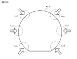
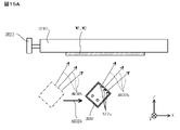
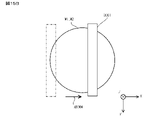
- this crack-and-opening method first, as shown by the arrow in FIG. 10A, the substrate W1 when a blade BL such as a razor blade is inserted from the peripheral edge of two substrates W1 and W2 bonded to each other into the bonded portion. , W2 peel length L is measured.
- the blade BL for example, a blade having a thickness of 100 ⁇ m is used. Further, as shown in FIG.
- the blade BL is inserted into six locations (Pos1, Pos2, Pos3, Pos4, Pos5, Pos6) on the peripheral edges of the two substrates W1 and W2 bonded to each other (see the arrow in FIG. 10B). ), The peeling length L from the blade contact was measured. Then, the strength of the bonding interface of the substrates W1 and W2 is calculated from the peeling length L at each of the six peripheral portions of the substrates W1 and W2 in terms of surface energy per unit area, whereby the substrates W1 and W2 are bonded. The strength was evaluated. When calculating the bonding strength (surface energy conversion) Eb from the peeling length L, the relational expression of the following equation (1) was used.
- Y indicates Young's modulus
- Ts indicates the thickness of the substrates W1 and W2
- Tb indicates the thickness of the blade BL.
- the Young's modulus Y was 6.5 ⁇ 10 10 [N / m 2 ]
- the thickness Ts of the substrates W1 and W2 was 0.0011 m (1. 1 mm)
- the thickness Tb of the blade BL was 0.0001 m (0.1 mm). From the calculation formula, the shorter the peeling length, the higher the bonding strength.
- Table 5 shows the average values of the peeling length and the bonding strength (in terms of surface energy) at the six points on the peripheral edges of the substrates W1 and W2, and the number of measurement points where bulk fracture occurred.
- the joint strength is such that less than 1 J / m 2 is insufficient strength, 1 J / m 2 or more is required, and 1.5 J / m 2 or more is a size that is usually judged to be a good product, and 2 J / m 2 . It is preferable to exceed the above, and it is more preferable to break the bulk.
- the evaluation results of the bonding strengths of the substrates W1 and W2 for the samples 1 to 20 are shown in Table 8 below.
- the column of “Sample name” corresponds to each of Samples 1 to 14 in Table 1 described above.
- the value in the column of “peeling length” indicates the average value of the peeling lengths at the six points ("Pos1" to “Pos6") of the peripheral portions of the two substrates W1 and W2 shown in FIG. 10B.
- the value in the column of "bonding strength (converted to surface energy)” is the bonding strength (converted to surface energy) at six locations ("Pos1" to "Pos6" on the peripheral edges of the two substrates W1 and W2 shown in FIG. 10B.
- the average value of the above is shown, and the estimated bonding strength is described for the ones in which bulk fracture occurred at all six locations on the peripheral edges of the two substrates W1 and W2. Further, the value in the column of "Number of bulk fracture locations" indicates the number of locations where bulk fracture has occurred among the six locations on the peripheral edges of the two substrates W1 and W2. For samples that have reached the bulk fracture strength (2.5 J / m 2 ), the peel length and the number of bulk fracture sites are compared. However, as the combination of the substrates W1 and W2, three types of combinations of SiO 2 substrate and Si substrate, glass substrates to each other, and Si substrate with oxide film to each other are adopted, so that the peeling length is simply changed when the bulk fracture strength is exceeded. Since it cannot be compared, the estimated joint strength is described.
- the bonding strength (in terms of surface energy) of Samples 1 and 2 was 2.5 J / m 2 or more, and there were 5 places where the bulk fracture strength was reached.
- the substrate W2 made of a Si substrate since a natural oxide film is not formed on the joint surface, an oxide film is formed on the joint surface by performing O 2 RIE treatment.
- the substrate W2 even if the N 2 RIE treatment is omitted, the N 2 radical treatment is performed on the joint surface, so that it is considered that the joint surface is in the above-mentioned N activated state.
- the samples 1 and 2 are subjected to the O 2 RIE treatment for forming an oxide film for hydrophilization on the bonding surface of the substrate W1 which is a Si substrate, but the N 2 RIE treatment is omitted. Nevertheless, since sufficient bonding strength is obtained, the bonding surface of the substrate W1 is in the above-mentioned N activated state by N 2 radical treatment without N 2 RIE treatment. it is conceivable that. That is, it was found that the N2 radical treatment greatly contributed to the realization of the N activated state at the junction surface of the substrates W1 and W2.
- the time required to expose the substrates W1 and W2 to the atmosphere in the load lock chamber 83 after the completion of the activation treatment is about 10 min, and from this, it is necessary to expose the substrates W1 and W2 to the atmosphere after the completion of the activation treatment. It was found that the longer the time, the lower the bonding strength of the substrates W1 and W2.
- the N 2 radical treatment contributes more to the bonding strength between the substrates W1 and W2 than the N 2 RIE treatment. understood. From this, it is considered that more OH groups formed on the junction surface of the substrates W1 and W2 in the N activated state are formed during the N2 radical treatment than during the N2 RIE treatment. Further, from the results of the bonding strength (in terms of surface energy) of the samples 8 and 9, a relatively large bonding strength can be obtained by performing the N 2 RIE treatment even when the N 2 radical treatment is not performed on the substrate W2. It turned out to be.
- the bonding strength in terms of surface energy
- the number of bulk fracture sites of samples 15 to 18 was as low as 0.48 J / m 2 in the case of O 2 RIE treatment alone, whereas the O 2 RIE treatment was performed.
- N 2 radical treatment is performed after N 2 radical treatment, it becomes 0.9 J / m 2
- N 2 radical treatment is performed after N 2 RIE treatment
- the bond strength is higher when 2.5 J / m 2 and nitrogen are used. It turned out to improve.
- the O 2 RIE treatment before the N 2 RIE treatment, the wettability between the substrates W1 and W2 is improved, the bonding strength between the substrates W1 and W2 is improved, and the space between the substrates W1 and W2 is improved.
- the voids generated in the area have been reduced. This is because the deposits such as organic substances adhering to the joint surfaces of the substrates W1 and W2 are removed by the O 2 RIE treatment, so that the substrate W1 in the N activated state in the subsequent N 2 RIE treatment and N 2 radical treatment. It is considered that this is due to the formation of many OH radicals on the joint surface of W2. Further, it is considered that the wettability of the joint surfaces of the substrates W1 and W2 is improved by removing the organic substances adhering to the joint surfaces of the substrates W1 and W2 by the O 2 RIE treatment.
- the bonding strength between the substrates was 0.59 J / m 2 , but by adopting the substrate bonding method according to the present embodiment, the bonding strength between the substrates is equal to or higher than the bulk fracture strength (2. It was found that it was significantly improved to 89 J / m 2 ).
- the substrates W1 and W2 are exposed to the atmosphere within a preset time, so that the substrate W1 and W2 are exposed to the atmosphere at 1 J / m. It was possible to obtain a joint strength that avoids a strength shortage of a level exceeding 2 .
- the bonding strength (in terms of surface energy) of the sample 21 was 0.31 J / m 2
- the bonding strength of the sample 22 corresponds to the bulk fracture strength. It was 0 J / m 2 , and it was found that the bonding strength of the sample 22 was significantly improved as compared with the sample 21.
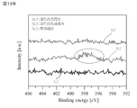
- the XPS X-ray photoelectron spectroscopy
- the N1s peak derived from oxynitride was detected in the vicinity of 396 eV to 399 eV, which was not observed. From this, it was found that SiON, which is an oxynitride, is formed on the joint surface of the substrates W1 and W2 by the activation treatment. Then, when the substrates W1 and W2 after the activation treatment were heat-treated under the same conditions as those of the heat treatment in the samples 21 and 22, the disappearance of the N1s peak disappeared as shown in the curves SL2 and SL3 in FIG. 12B. confirmed. Since this and, as shown in FIG.
- the bonding strength of the sample 22 is significantly improved as compared with the bonding strength of the sample 21, in the sample 22, the oxynitride (SiON) is hydrogen at the bonding portion of the substrates W1 and W2. It is considered that it is substituted with an OH group that contributes to the bond.
- SiON oxynitride
- reactive ion etching using nitrogen gas and irradiation of nitrogen radicals are performed on the bonding surfaces of the two substrates W1 and W2 to be bonded to each other.
- the joint surfaces of the substrates W1 and W2 are activated.
- the N-active state of the joint surfaces of the substrates W1 and W2 formed thereby is unstable, and the active state is inactivated as it is, so that the strength is reduced. In order to avoid this, it is necessary to activate the joint surfaces of the substrates W1 and W2 and then bring them into contact with water molecules within a preset reference time.
- the bonding surfaces of the substrates W1 and W2 are exposed to the atmosphere or water gas within a preset reference time. do.
- the joint surfaces of the substrates W1 and W2 can be brought into contact with water molecules in an N-active state, so that many oxynitrides can be formed on the joint surfaces of the substrates W1 and W2.
- the bonding surfaces of the substrates W1 and W2 are brought into contact with each other to temporarily bond the substrates W1 and W2 and then heat treatment is performed, many oxynitrides existing between the bonding surfaces of the substrates W1 and W2 become OH groups.
- OH groups are generated for the first time by temporarily bonding the substrates W1 and W2 and then performing a heat treatment, and the bonding strength between the substrates W1 and W2 is improved.
- a large number of oxynitrides (N groups) are generated on the bonding surface by subjecting the bonding surface of the substrates W1 and W2 to an activation treatment.
- N groups oxynitrides
- the joint surface of the substrate is subjected to RIE treatment to improve the wettability of the joint surface, and then water is sprayed on the joint surface to clean the joint surface, and then the joint surface is cleaned.
- Temporary bonding is performed by bringing the bonding surfaces of two substrates into contact with each other with water molecules interposed between the bonding surfaces of the substrates under atmospheric pressure. Then, it was common to join the two substrates by heat-treating the two substrates temporarily bonded to each other.
- the treatment temperature at the time of heat treatment it was necessary to set the treatment temperature at the time of heat treatment to about 350 ° C.
- the two substrates are brought into contact with each other in a state where the central portion of at least one of the two substrates is pressed and bent, so that the two substrates are brought into contact with each other.
- Technology that suppresses the entrainment of air between them is often adopted.
- the conductor pattern is formed on the substrate, the wetting speed of the substrate becomes location-dependent due to the conductor pattern, and the generation of voids due to the entrainment of air between the two substrates is reduced. Sometimes I could't.
- FIG. 13 (A-2) when the substrate is heated with water molecules interposed between the bonding surfaces of the two substrates, as shown in FIG. 13 (A-3),
- the water molecule attached to the substrate changes to an OH group and changes to a strong covalent bond.
- FIG. 13 (A-1) when water molecules are attached to the bonding surface and then the substrate is placed under reduced pressure, FIG. 13 (B-).
- FIG. 13 (B-) when water molecules are attached to the bonding surface and then the substrate is placed under reduced pressure, FIG. 13 (B-).
- FIG. 13 (B-) As shown in 2), the water molecules adhering to the substrate evaporate, and the water molecules on the substrate decrease.
- the number of OH groups formed on the bonding surface of the substrate is reduced, and as shown in FIG.
- the substrates are bonded to each other with almost no OH groups formed on the bonding surface of the substrate. Will be done. In this case, it was difficult to firmly join the substrates.
- the bonding strength is 1 J because the oxide film has low density. It did not exceed / m 2 .
- FIG. 13 (C-1) OH groups are formed on the bonding surfaces of the substrates W1 and W2 in the activation treatment. Therefore, even if the water molecules adhering to the substrates W1 and W2 evaporate under reduced pressure thereafter, as shown in FIG. 13 (C-2), a relatively large number of OH groups are present on the bonding surface of the substrates W1 and W2. The formed state is maintained. Therefore, as shown in FIG. 13 (C-3), the two substrates are bonded to each other via a strong covalent bond by performing a heat treatment after hydrogen-bonding the two substrates via an OH group to temporarily bond them. Be joined.
- the substrates W1 and W2 can be firmly bonded to each other under reduced pressure. Therefore, the substrates W1 and W2 can be firmly bonded to each other while suppressing the entrainment of air between the substrates W1 and W2 or the generation of voids caused by the water remaining on the bonding surface of the substrates W1 and W2.
- the heat treatment temperature be less than 200 ° C, preferably about 150 ° C.
- the heat treatment after temporarily bonding the substrates W1 and W2 is performed at a processing temperature of 150 ° C. and a processing time of 7.
- High bonding strength can be obtained by performing under the condition of time. That is, high bonding strength can be ensured even when the heat treatment treatment temperature is 150 ° C. or lower.
- the substrates W1 and W2 have been exposed to the atmosphere after being transported from the second transport device 84 to the load lock chamber 83 under reduced pressure after the activation treatment in the activation treatment device 2 is completed. In this case, it took about 10 minutes for the substrates W1 and W2 to be exposed to the atmosphere, and sufficient bonding strength could not be obtained.
- the substrate bonding system according to the present embodiment after the activation treatment in the activation treatment device 2 is completed, the substrate bonding system is exposed to the atmosphere in the activation treatment device 2 or the second transfer device 84. The time from the completion of the activation treatment to the exposure to the atmosphere is shortened, and the bonding strength between the substrates W1 and W2 can be increased.
- the bonding strength between the substrates W1 and W2 can be further increased by exposing the substrates W1 and W2 to water gas in the activation treatment device 2 or the second transfer device 84. can. Further, even if the inside of the chamber 212 is once decompressed after being exposed to water gas in the activation treatment apparatus 2, the chamber 212 is transported to the load lock chamber 83 under the decompression state, and then exposed to the atmosphere for being put into the cleaning apparatus 3. Bulk fracture occurred, and there was no significant difference in the bonding strength between the substrates W1 and W2.
- the OH groups formed on the joint surfaces of the substrates W1 and W2 in the N-activated state did not disappear even when placed under reduced pressure. Further, when the joint surfaces of the substrates W1 and W2 are exposed to water gas, if a few percent of water molecules are filled in the chamber 212 without supplying water gas having the same level as atmospheric pressure into the chamber 212. It was also found that many OH groups were formed on the joint surfaces of the substrates W1 and W2. In this case, the tact of the device can be shortened because the activation treatment device 2 only exposes water and gas for a short time and the vacuum transfer can be performed as it is without returning to the atmospheric pressure.
- the substrates W1 and W2 are transported from the cleaning device 3 to the substrate bonding device 1, the substrates W1 and W2 are transported under a reduced pressure of about 1 Pa, and the substrate W1 is transported under a pressure of about 1 Pa in the substrate bonding device 1. , W2 was joined.
- the wafer bonding system is transported from the cleaning device 3 to the wafer bonding device 1 under an atmospheric pressure of 10 Pa or more and 1000 Pa or less. As a result, evaporation of water molecules adhering to the substrates W1 and W2 is suppressed, and the bonding strength between the substrates W1 and W2 can be increased.
- the bonding process of the substrate bonding device 1 water molecules can be left on the bonding surface of the substrates W1 and W2, and the bonding surface of the substrates W1 and W2 is activated by N activation treatment by the activation processing device 2.
- the water molecules remaining on the bonding surface can form more OH groups on the bonding surface. Therefore, the bonding strength between the substrates W1 and W2 can be further increased. Further, in the activation treatment, the same result was obtained even when only the treatment using oxygen gas was performed without performing the etching treatment using nitrogen gas and the irradiation with nitrogen radicals.
- the present invention is not limited to the configuration of the above-described embodiments.
- it may be provided with a water gas supply unit (not shown) for supplying water gas into the load lock chamber 83 or the second transfer device 84.
- the water gas supply unit generates and supplies water gas by mixing carrier gas such as argon (Ar), nitrogen (N 2 ), helium (He), and oxygen (O 2 ) with vaporized water.
- carrier gas such as argon (Ar), nitrogen (N 2 ), helium (He), and oxygen (O 2 )
- the water gas supply unit is connected to the load lock chamber 83 via a supply valve and a supply pipe. The flow rates of the water gas and the carrier gas introduced into the load lock chamber 83 are adjusted by controlling the opening degree of the supply valve.
- the water gas supply unit may be configured to accelerate water ( H2O ) molecules, clusters, and the like to irradiate the joint surfaces of the substrates W1 and W2.
- the water gas supply unit may be composed of a particle beam source that radiates accelerated water ( H2O ) particles.
- the particle beam source may be configured to generate water gas by using, for example, an ultrasonic wave generating element.
- a mixed gas of water ( H2O ) and a carrier gas generated by the above-mentioned bubbling or ultrasonic vibration into the above-mentioned particle beam source, a water particle beam is generated to generate a substrate W1.
- W2 may be configured to irradiate the joint surface.
- the load lock chamber 83 may be opened to the atmosphere after the joint surfaces of the substrates W1 and W2 are exposed to water gas without opening the load lock chamber 83 to the atmosphere. Further, instead of water gas, a gas containing H and OH groups may be supplied to the joint surfaces of the substrates W1 and W2.
- the activation processing device may have a particle beam source that activates the joint surface of the substrates W1 and W2 by irradiating the substrates W1 and W2 with the particle beam.
- the activation processing apparatus 3002 according to the present modification has a chamber 3212, a stage 3210 for holding the substrates W1 and W2, a particle beam source 3061, and a beam source transport unit 3063. ..
- the same reference numerals as those in FIG. 2 are attached to the same configurations as those in the embodiment.
- the activation processing device 3002 has a plasma chamber 3213, an induction coil 215, and a high frequency power supply 216.
- the activation processing apparatus 3002 has a stage drive unit 3623 that rotationally drives the stage 3210 around one axis orthogonal to the thickness direction as shown by the arrow AR303 in FIG.
- the stage 3210 has, for example, a vacuum chuck, and when the substrates W1 and W2 are charged, the stages W1 and W2 are adsorbed and held.
- the particle beam source 3061 is, for example, a high-speed atomic beam (FAB, Fast Atom Beam) source, and is a discharge chamber 3612, an electrode 3611 arranged in the discharge chamber 3612, a beam source drive unit 3613, and a nitrogen gas discharge chamber. It has a gas supply unit 3614 for supplying into the 3612.
- a FAB emission port 3612a that emits neutral atoms is provided on the peripheral wall of the discharge chamber 3612.
- the discharge chamber 3612 is made of a carbon material.
- the discharge chamber 3612 has a long box shape, and a plurality of FAB radiation ports 3612a are arranged side by side in a straight line along the longitudinal direction thereof.
- the beam source drive unit 3613 is a DC power supply (FIG.) that applies a DC voltage between the plasma generation unit (not shown) that generates nitrogen gas plasma in the discharge chamber 3612 and the peripheral wall of the electrode 3611 and the discharge chamber 3612. Not shown) and.
- the beam source drive unit 3613 applies a DC voltage between the peripheral wall of the discharge chamber 3612 and the electrode 3611 in a state where plasma of nitrogen gas is generated in the discharge chamber 3612. At this time, nitrogen ions in the plasma are attracted to the peripheral wall of the discharge chamber 3612.
- the nitrogen ion toward the FAB emission port 3612a receives an electron from the peripheral wall of the discharge chamber 3612 formed of the carbon material on the outer peripheral portion of the FAB emission port 3612a as it passes through the FAB emission port 3612a. Then, the nitrogen ions become electrically neutralized nitrogen atoms and are released to the outside of the discharge chamber 3612. However, some of the nitrogen ions cannot receive electrons from the peripheral wall of the discharge chamber 3612, and are discharged as nitrogen ions to the outside of the discharge chamber 3612. Further, a part or all of the inside of the FAB housing may be formed of Si. By doing so, Si particles are emitted at the same time as the Ar beam, so Si is driven into the interface, and OH groups are also attached to the shot Si, so more OH groups can be generated and the bonding strength can be increased. can.
- the beam source transport portion 3063 is long and is inserted into a hole 3212a provided in the chamber 3212 to support a support rod 3631 at one end to support the particle beam source 3061 and a support rod 3631 at the other end of the support rod 3631. It has a support body 3632 and a support body driving unit 3633 for driving the support body 3632. Further, the beam source transport unit 3063 has a bellows 3634 interposed between the outer peripheral portion of the hole 3212a of the chamber 3212 and the support 3632 in order to maintain the degree of vacuum in the chamber 3212.
- the support drive unit 3633 drives the support 3632 in the direction in which the support rod 3631 is inserted and removed into the chamber 3212, as shown by the arrow AR301 in FIG.
- the beam source transport unit 3063 moves the particle beam source 3061 in a direction orthogonal to the arrangement direction of the plurality of FAB emission ports 3612a.
- the activation processing device 3002 has a nitrogen gas supply unit 220A that supplies nitrogen gas into the chamber 3212 via the supply pipe 223A. Then, when a high frequency current is supplied to the induction coil 215 with the N 2 gas introduced into the plasma chamber 213, the plasma PLM 2 is formed in the plasma chamber 213. At this time, only the radicals contained in the plasma PLM2 generated in the plasma chamber 213 flow down to the lower side of the plasma chamber 213 in the chamber 3212.
- the pressure in the chamber 64 is evacuated to 10-3 Pa by using a turbo molecular pump, for example, but during radical treatment, the pressure in the chamber 64 is reduced to several tens of Pa. Raise it.
- the particle beam source 3061 irradiates the junction surface of the substrates W1 and W2 with the particle beam in the X-axis direction. I will move it.
- the activation processing apparatus 3002 irradiates the junction surface of the substrates W1 and W2 with the particle beam while moving the particle beam source 3061 in the + X direction, and then moves the particle beam source 3061 in the ⁇ X direction to the substrate.
- a particle beam is applied to the joint surface of W1 and W2.
- the moving speed of the particle beam source 3061 is set to, for example, 1.2 to 14.0 mm / sec.
- the power supplied to the particle beam source 3061 is set to, for example, 1 kV and 100 mA.
- the flow rate of nitrogen gas or oxygen gas introduced into the discharge chamber 3612 of the particle beam source 3061 is set to, for example, 100 sccm.
- the activation processing apparatus 3002 reverses the stage 3210 so that the joint surfaces of the substrates W1 and W2 face vertically upward. Then, as shown by the arrow AR307 in FIG. 16B, the activation processing apparatus 3002 irradiates the junction surface of the substrates W1 and W2 with nitrogen radicals.
- the bonding surface of the substrates W1 and W2 is a so-called hybrid bonding surface composed of, for example, a region formed of Cu as an electrode and a region formed of an oxide film serving as an insulating layer
- a conventional plasma When the RIE treatment is performed in, a sheath region is formed in the vicinity of the joint surfaces of the substrates W1 and W2, and all the ionized ones are drawn in and attack the joint surfaces of the substrates W1 and W2.
- the bonding strength at the oxide film decreases. It ends up.
- the electric resistance of the electrode increases.
- the plasma generated in the chamber 3212 is irradiated with the beam, so that the region made of Cu or the region formed from the oxide film is formed.
- the Cu ions, Cu particles, or particles made of the insulating film material generated by etching are repelled without returning to the bonding surface of the substrates W1 and W2.
- the resin constituting the adhesive sheet is the chip. It adheres to the joint surface.
- the resin constituting the pressure-sensitive adhesive sheet does not adhere to the joint surface of the chip, and a good activation treatment can be performed.
- the activation processing device 2 has described an example in which the plasma generation source generates ICP, but the present invention is not limited to this, and the plasma generation source generates plasma by microwaves. May be.
- the activation processing device 4002 according to the present modification includes a stage 210, a chamber 4212, a trap plate 4214, a waveguide 4215, a magnetron 4216, and a bias application unit 217. Have.
- the same reference numerals as those in FIG. 2 are attached to the same configurations as those of the activation processing apparatus 2 according to the embodiment.
- the activation treatment device 4002 has a nitrogen gas supply unit 220A and an oxygen gas supply unit 220B.
- the nitrogen gas supply unit 220A has a nitrogen gas storage unit 221A, a supply valve 222A, and a supply pipe 223A.
- the oxygen gas supply unit 220B includes an oxygen gas storage unit 221B, a supply valve 222B, and a supply pipe 223B.
- the substrates W1 and W2 are placed on the stage 210.
- the chamber 4212 is connected to the waveguide 4215 via a glass window 4213.
- the chamber 4212 is connected to the vacuum pump 201 via the exhaust pipe 202A and the exhaust valve 203A.
- the trap plate 4214 is formed of, for example, metal, graphite, etc., and is maintained at the ground potential.
- the microwave generated by the magnetron 4216 is introduced into the chamber 4212 through the waveguide 4215.
- the magnetron 4216 for example, one that generates a microwave having a frequency of 2.45 GHz can be adopted.
- the plasma PLM is formed in the vicinity of the glass window 4213 in the chamber 4212 by the microwaves.
- the trap plate 4214 traps the ions contained in the plasma PLM and causes only the radicals to flow down to the stage 210.
- Plasma PLM is generated in the chamber 4212 from the magnetron 4216, the nitrogen gas supply unit 220A, and the trap plate 4214, and N2 () radicals in the plasma are supplied to the junction surface of the substrates W1 and W2 supported by the stage 210.
- the plasma source is configured.
- this activation processing apparatus 4002 while applying a bias to the stage 210 by the bias applying unit 217, nitrogen gas and oxygen gas are introduced from the upper part of the chamber 4212 to physically etch the substrates W1 and W2 (RIE processing). ) Is possible. Further, in this activation processing apparatus 4002, ions or radicals are generated at high density in the upper part of the chamber 4212 by the microwave introduced in the upper part of the chamber 4212, and the ions are generated when passing through the trap plate 4214 maintained at the ground potential. Only the radicals trapped and containing neutrons are downflowed to the stage 210 side of the chamber 4212 to chemically treat the substrates W1 and W2 on the stage 210.
- the activation treatment device 2 applies a bias voltage to the stage 210 by the bias application unit 217 while introducing nitrogen gas and oxygen gas from the upper part of the chamber 212 during the RIE treatment, and during the radical treatment,
- a bias voltage to the stage 210 by the bias application unit 217 while introducing nitrogen gas and oxygen gas from the upper part of the chamber 212 during the RIE treatment, and during the radical treatment.
- a trap plate (not shown) may be arranged between the stage 210 and the inner region of the plasma chamber 213.
- the trap plate is maintained at, for example, a ground potential.
- the activation treatment apparatus 2 since the ions are trapped in the ICP plasma by the electric field formed in the plasma chamber 213 by the induction coil 215 at the time of the radical treatment, there is no trap plate. Only radicals can be downflowed to the stage 210 side. However, in the radical treatment, the ions are not completely trapped in the ICP plasma, and a certain number of ions fall to the stage 210 side. On the other hand, in the activation treatment apparatus according to the present modification, since the ions are trapped by the trap plate in the radical treatment, it is possible to suppress the irradiation of the ions to the stage 210 side.
- the current can be continuously supplied to the induction coil 215 during both the RIE treatment and the radical treatment, so that the radical treatment can be performed from the RIE treatment. It is not necessary to significantly switch the current supply to the induction coil 215 at the time of switching to. Therefore, the tact required for the RIE treatment and the radical treatment of the substrates W1 and W2 can be shortened, or more ions or radicals can be generated.
- the trap plate is maintained at the ground potential, but the present invention is not limited to this.
- the trap plate may be maintained at the ground potential.
- the ions in the plasma PLM generated in the plasma chamber 213 fall to the stage 210 side without being trapped by the trap plate during the RIE treatment, and are trapped by the trap plate only during the radical treatment.
- the radicals will be irradiated to the stage 210 along with the flow of nitrogen gas and oxygen gas during the radical treatment.
- the radical treatment the ions in the plasma PLM generated in the plasma chamber 213 are drawn into the trap plate and accelerated, and when passing through the holes of the trap plate, electrons are emitted from the trap plate.
- the substrates W1 and W2 placed on the stage 210 are irradiated. Therefore, it is possible to irradiate the substrates W1 and W2 with radicals containing more neutrons.
- the stage 210 may be maintained at the ground potential without applying a bias, and the trap plate may be maintained in a floating state.
- the ions in the plasma PLM generated in the plasma chamber 213 pass through the holes of the trap plate as they are and are irradiated to the substrates W1 and W2 mounted on the stage 210 in a state of being accelerated toward the stage 210 side. To. Therefore, a process similar to the RIE process is performed. Then, if the trap plate is maintained at the ground potential, ions are trapped in the trap plate and only radicals pass through the trap plate to irradiate the substrates W1 and W2 mounted on the stage 210.
- the trap plate is kept in a floating state without being maintained at the ground potential, and the trap plate is maintained at the ground potential only during the radical treatment, or the trap plate is maintained at the ground potential without applying a bias to the stage 210.
- the configuration for maintaining the trap plate in a floating state is not limited to the so-called activation processing apparatus using ICP plasma, and is the so-called activation processing apparatus using microwaves or parallel to be described with reference to FIG. It may be applied in a flat plate type activation processing apparatus. In this case, the configuration can be cheaper.
- the parallel plate type activation processing device for example, as shown in FIG.
- an electrode 6215 arranged in the plasma chamber 213, a bias applying portion 6216 for applying a bias to the electrode 6215, and a trap plate 5214 are used.
- the activation processing apparatus 6002 having the above can be mentioned.
- ions are trapped in the electric field in the sheath region of the plasma.
- the bias frequency is 13.56 MHz, but it is more effective to use a bias with a frequency of 27 MHz or a microwave with a frequency of 2 GHz, such as a parallel plate type or ICP plasma, because more radicals can be generated. be.
- the ions in the plasma PLM are trapped by the sheath region formed in the plasma chamber 213 or the electric field formed by the induction coil 215 and do not fall to the stage 210 side. Therefore, if the trap plate is maintained at the ground potential, the positive ions in the plasma PLM are attracted to the trap plate and accelerated, and when passing through the hole of the trap plate, electrons are received from the trap plate and accelerated as neutrons in the stage 210.
- the substrates W1 and W2 placed on the above are irradiated. Therefore, damage to the substrates W1 and W2 caused by charge-up by ions can be reduced.
- the trap plate in a floating state, the ions in the plasma PLM are maintained in a state of being trapped in the sheath region formed in the plasma chamber 213 or the electric field formed by the induction coil 215, so that the plasma PLM is maintained.
- Chemical treatment is possible by dropping only the radicals inside through the trap plate to the stage 210 side.
- the trap plate or the stage 210 is not limited to being maintained at the ground potential, and a bias voltage may be applied. As a result, the ions passing through the trap plate can be further accelerated to increase their energy.
- N 2 RIE treatment and N 2 radical treatment are performed on both of the two substrates W1 and W2
- activation treatment is performed on both the bonding surfaces of the two substrates W1 and W2. If there is, it is not limited to this activation treatment method.
- only one of the two substrates W1 and W2 is subjected to N 2 RIE treatment and N 2 radical treatment, and the other is activated so that at least one of N 2 RIE treatment and N 2 radical treatment is not performed. May be.
- the substrate bonding apparatus 1 applies pressure to the substrates W1 and W2 and heat-treats the substrates W1 and W2 in a state where the entire bonding surfaces of the substrates W1 and W2 are in contact with each other.
- the substrate bonding apparatus 1 may have a configuration in which the entire bonding surfaces of the substrates W1 and W2 are in contact with each other, and only pressure is applied to the substrates W1 and W2 without heat treatment.
- the substrate bonding apparatus 1 may be configured to perform only the heat treatment of the substrates W1 and W2 without applying pressure while the entire bonding surfaces of the substrates W1 and W2 are in contact with each other.
- the substrates W1 and W2 may be pressurized and heat-treated in an apparatus different from the substrate bonding apparatus 1.
- the substrate bonding apparatus 1 may execute up to the temporary bonding of the substrates W1 and W2, and then heat treatment may be performed in another heating apparatus (not shown).
- the present invention is not limited to this, and the configurations in which the substrates W1 and W2 are joined under atmospheric pressure may be used, or may be arbitrary. It may be configured to join in an atmosphere filled with the gas of.
- the present invention is not limited to this, and the load lock chamber 83 is provided with the cooling device. It may not have a configuration.
- the activation processing device 3002 is provided with the particle beam source 3061
- the present invention is not limited to this, and for example, the inversion device 4 may be provided with the particle beam source.
- the present invention is suitable for manufacturing, for example, CMOS (Complementary MOS) image sensors, memories, arithmetic elements, and MEMS (Micro Electro Mechanical Systems).
- CMOS Complementary MOS
- MEMS Micro Electro Mechanical Systems
Landscapes
- Engineering & Computer Science (AREA)
- Physics & Mathematics (AREA)
- Fluid Mechanics (AREA)
- Mechanical Engineering (AREA)
- Condensed Matter Physics & Semiconductors (AREA)
- General Physics & Mathematics (AREA)
- Manufacturing & Machinery (AREA)
- Computer Hardware Design (AREA)
- Microelectronics & Electronic Packaging (AREA)
- Power Engineering (AREA)
- Pressure Welding/Diffusion-Bonding (AREA)
- Combinations Of Printed Boards (AREA)
Priority Applications (5)
| Application Number | Priority Date | Filing Date | Title |
|---|---|---|---|
| EP21875137.8A EP4224512A1 (en) | 2020-09-30 | 2021-09-10 | Substrate bonding method and substrate bonding system |
| JP2022553755A JP7440047B2 (ja) | 2020-09-30 | 2021-09-10 | 基板接合方法および基板接合システム |
| US18/245,895 US12409644B2 (en) | 2020-09-30 | 2021-09-10 | Substrate bonding method and substrate bonding system |
| TW110134185A TW202230457A (zh) | 2020-09-30 | 2021-09-14 | 基板接合方法及基板接合系統 |
| JP2023194100A JP2024009082A (ja) | 2020-09-30 | 2023-11-15 | 基板接合方法および基板接合システム |
Applications Claiming Priority (2)
| Application Number | Priority Date | Filing Date | Title |
|---|---|---|---|
| JP2020164962 | 2020-09-30 | ||
| JP2020-164962 | 2020-09-30 |
Publications (1)
| Publication Number | Publication Date |
|---|---|
| WO2022070835A1 true WO2022070835A1 (ja) | 2022-04-07 |
Family
ID=80950377
Family Applications (1)
| Application Number | Title | Priority Date | Filing Date |
|---|---|---|---|
| PCT/JP2021/033291 Ceased WO2022070835A1 (ja) | 2020-09-30 | 2021-09-10 | 基板接合方法および基板接合システム |
Country Status (5)
| Country | Link |
|---|---|
| US (1) | US12409644B2 (enExample) |
| EP (1) | EP4224512A1 (enExample) |
| JP (2) | JP7440047B2 (enExample) |
| TW (1) | TW202230457A (enExample) |
| WO (1) | WO2022070835A1 (enExample) |
Families Citing this family (2)
| Publication number | Priority date | Publication date | Assignee | Title |
|---|---|---|---|---|
| CN209933070U (zh) | 2018-01-07 | 2020-01-14 | 苏州杰成医疗科技有限公司 | 心脏瓣膜假体 |
| JP2025144080A (ja) * | 2024-03-19 | 2025-10-02 | 株式会社Screenホールディングス | 基板接合方法および基板接合装置 |
Citations (12)
| Publication number | Priority date | Publication date | Assignee | Title |
|---|---|---|---|---|
| JPH04206719A (ja) * | 1990-11-30 | 1992-07-28 | Tokyo Electron Ltd | 基板処理装置および基板処理方法 |
| JPH06302486A (ja) * | 1993-02-16 | 1994-10-28 | Nippondenso Co Ltd | 2つの材料の直接接合方法及び材料直接接合装置 |
| JP2005079353A (ja) | 2003-08-29 | 2005-03-24 | Tadatomo Suga | 基板接合方法、照射方法、および基板接合装置 |
| JP2005311298A (ja) * | 2004-01-22 | 2005-11-04 | Bondotekku:Kk | 接合方法及びこの方法により作成されるデバイス並びに接合装置 |
| JP2006080314A (ja) * | 2004-09-09 | 2006-03-23 | Canon Inc | 結合基板の製造方法 |
| JP2006339363A (ja) * | 2005-06-01 | 2006-12-14 | Bondtech Inc | 表面活性化方法および表面活性化装置 |
| JP2007281166A (ja) * | 2006-04-06 | 2007-10-25 | Matsushita Electric Ind Co Ltd | 接合方法および接合装置ならびに接合基板 |
| JP2008202114A (ja) * | 2007-02-21 | 2008-09-04 | Canon Anelva Corp | 薄膜作成装置 |
| JP2009118034A (ja) * | 2007-11-05 | 2009-05-28 | Epson Toyocom Corp | 直接接合用ウェハ |
| WO2018084285A1 (ja) * | 2016-11-07 | 2018-05-11 | ボンドテック株式会社 | 基板接合方法、基板接合システムおよび親水化処理装置の制御方法 |
| WO2020044579A1 (ja) * | 2018-08-31 | 2020-03-05 | ボンドテック株式会社 | 接合システムおよび接合方法 |
| JP2020164962A (ja) | 2019-03-29 | 2020-10-08 | Jx金属株式会社 | 電解装置及び電解方法 |
Family Cites Families (4)
| Publication number | Priority date | Publication date | Assignee | Title |
|---|---|---|---|---|
| US6780759B2 (en) * | 2001-05-09 | 2004-08-24 | Silicon Genesis Corporation | Method for multi-frequency bonding |
| JP4967842B2 (ja) | 2007-06-18 | 2012-07-04 | セイコーエプソン株式会社 | シリコン基材の接合方法、液滴吐出ヘッド、液滴吐出装置および電子デバイス |
| IN2015DN03311A (enExample) * | 2012-09-28 | 2015-10-09 | Dainippon Printing Co Ltd | |
| JP6395333B2 (ja) | 2014-04-25 | 2018-09-26 | 須賀 唯知 | 基板接合装置および基板接合方法 |
-
2021
- 2021-09-10 JP JP2022553755A patent/JP7440047B2/ja active Active
- 2021-09-10 WO PCT/JP2021/033291 patent/WO2022070835A1/ja not_active Ceased
- 2021-09-10 US US18/245,895 patent/US12409644B2/en active Active
- 2021-09-10 EP EP21875137.8A patent/EP4224512A1/en not_active Withdrawn
- 2021-09-14 TW TW110134185A patent/TW202230457A/zh unknown
-
2023
- 2023-11-15 JP JP2023194100A patent/JP2024009082A/ja active Pending
Patent Citations (12)
| Publication number | Priority date | Publication date | Assignee | Title |
|---|---|---|---|---|
| JPH04206719A (ja) * | 1990-11-30 | 1992-07-28 | Tokyo Electron Ltd | 基板処理装置および基板処理方法 |
| JPH06302486A (ja) * | 1993-02-16 | 1994-10-28 | Nippondenso Co Ltd | 2つの材料の直接接合方法及び材料直接接合装置 |
| JP2005079353A (ja) | 2003-08-29 | 2005-03-24 | Tadatomo Suga | 基板接合方法、照射方法、および基板接合装置 |
| JP2005311298A (ja) * | 2004-01-22 | 2005-11-04 | Bondotekku:Kk | 接合方法及びこの方法により作成されるデバイス並びに接合装置 |
| JP2006080314A (ja) * | 2004-09-09 | 2006-03-23 | Canon Inc | 結合基板の製造方法 |
| JP2006339363A (ja) * | 2005-06-01 | 2006-12-14 | Bondtech Inc | 表面活性化方法および表面活性化装置 |
| JP2007281166A (ja) * | 2006-04-06 | 2007-10-25 | Matsushita Electric Ind Co Ltd | 接合方法および接合装置ならびに接合基板 |
| JP2008202114A (ja) * | 2007-02-21 | 2008-09-04 | Canon Anelva Corp | 薄膜作成装置 |
| JP2009118034A (ja) * | 2007-11-05 | 2009-05-28 | Epson Toyocom Corp | 直接接合用ウェハ |
| WO2018084285A1 (ja) * | 2016-11-07 | 2018-05-11 | ボンドテック株式会社 | 基板接合方法、基板接合システムおよび親水化処理装置の制御方法 |
| WO2020044579A1 (ja) * | 2018-08-31 | 2020-03-05 | ボンドテック株式会社 | 接合システムおよび接合方法 |
| JP2020164962A (ja) | 2019-03-29 | 2020-10-08 | Jx金属株式会社 | 電解装置及び電解方法 |
Also Published As
| Publication number | Publication date |
|---|---|
| JP7440047B2 (ja) | 2024-02-28 |
| US12409644B2 (en) | 2025-09-09 |
| JP2024009082A (ja) | 2024-01-19 |
| US20240009984A1 (en) | 2024-01-11 |
| TW202230457A (zh) | 2022-08-01 |
| EP4224512A1 (en) | 2023-08-09 |
| JPWO2022070835A1 (enExample) | 2022-04-07 |
Similar Documents
| Publication | Publication Date | Title |
|---|---|---|
| JP6617227B2 (ja) | 基板接合装置および基板接合方法 | |
| JP6388272B1 (ja) | 基板接合方法、基板接合システムおよび親水化処理装置の制御方法 | |
| JP6994210B2 (ja) | 接合システムおよび接合方法 | |
| CN101622692B (zh) | 等离子体处理装置的清洗方法、执行该清洗方法的等离子体处理装置 | |
| JP2024009082A (ja) | 基板接合方法および基板接合システム | |
| JP6429179B2 (ja) | 基板接合装置および基板接合方法 | |
| CN101556430A (zh) | 掩膜表面化学处理方法及系统 | |
| JPWO2003048864A1 (ja) | マスク形成方法及び除去方法、並びに該手法により製造された半導体デバイス、電気回路、表示体モジュール、カラーフィルタ及び発光素子 | |
| WO2022025160A1 (ja) | チップ接合システムおよびチップ接合方法 | |
| JP2024056041A (ja) | 接合方法 | |
| WO2022158520A1 (ja) | 接合方法、接合装置および接合システム | |
| JP6067210B2 (ja) | プラズマ処理装置 | |
| JP7780236B1 (ja) | 粒子ビーム源、接合システムおよび接合方法 | |
| CN117121158A (zh) | 接合方法、接合装置及接合系统 | |
| JP2025087176A (ja) | 接合方法、構造体および接合システム | |
| JP6174210B2 (ja) | 載置台およびプラズマ処理装置 | |
| WO2024147351A1 (ja) | 接合方法、接合システム、照射装置および活性化処理装置 | |
| JP6366307B2 (ja) | 洗浄システム、および洗浄方法 | |
| JP2017183611A (ja) | プラズマ処理方法、およびプラズマ処理装置 |
Legal Events
| Date | Code | Title | Description |
|---|---|---|---|
| 121 | Ep: the epo has been informed by wipo that ep was designated in this application |
Ref document number: 21875137 Country of ref document: EP Kind code of ref document: A1 |
|
| ENP | Entry into the national phase |
Ref document number: 2022553755 Country of ref document: JP Kind code of ref document: A |
|
| WWE | Wipo information: entry into national phase |
Ref document number: 18245895 Country of ref document: US |
|
| NENP | Non-entry into the national phase |
Ref country code: DE |
|
| ENP | Entry into the national phase |
Ref document number: 2021875137 Country of ref document: EP Effective date: 20230502 |
|
| WWG | Wipo information: grant in national office |
Ref document number: 18245895 Country of ref document: US |