EP4184580A1 - Speicher und herstellungsverfahren dafür - Google Patents
Speicher und herstellungsverfahren dafür Download PDFInfo
- Publication number
- EP4184580A1 EP4184580A1 EP20949449.1A EP20949449A EP4184580A1 EP 4184580 A1 EP4184580 A1 EP 4184580A1 EP 20949449 A EP20949449 A EP 20949449A EP 4184580 A1 EP4184580 A1 EP 4184580A1
- Authority
- EP
- European Patent Office
- Prior art keywords
- gate
- groove
- conductive layer
- substrate
- memory
- Prior art date
- Legal status (The legal status is an assumption and is not a legal conclusion. Google has not performed a legal analysis and makes no representation as to the accuracy of the status listed.)
- Pending
Links
Images








Classifications
-
- H—ELECTRICITY
- H10—SEMICONDUCTOR DEVICES; ELECTRIC SOLID-STATE DEVICES NOT OTHERWISE PROVIDED FOR
- H10B—ELECTRONIC MEMORY DEVICES
- H10B12/00—Dynamic random access memory [DRAM] devices
- H10B12/30—DRAM devices comprising one-transistor - one-capacitor [1T-1C] memory cells
- H10B12/34—DRAM devices comprising one-transistor - one-capacitor [1T-1C] memory cells the transistor being at least partially in a trench in the substrate
-
- H—ELECTRICITY
- H10—SEMICONDUCTOR DEVICES; ELECTRIC SOLID-STATE DEVICES NOT OTHERWISE PROVIDED FOR
- H10B—ELECTRONIC MEMORY DEVICES
- H10B12/00—Dynamic random access memory [DRAM] devices
- H10B12/01—Manufacture or treatment
- H10B12/02—Manufacture or treatment for one transistor one-capacitor [1T-1C] memory cells
- H10B12/05—Making the transistor
- H10B12/053—Making the transistor the transistor being at least partially in a trench in the substrate
-
- H—ELECTRICITY
- H10—SEMICONDUCTOR DEVICES; ELECTRIC SOLID-STATE DEVICES NOT OTHERWISE PROVIDED FOR
- H10B—ELECTRONIC MEMORY DEVICES
- H10B12/00—Dynamic random access memory [DRAM] devices
-
- H—ELECTRICITY
- H10—SEMICONDUCTOR DEVICES; ELECTRIC SOLID-STATE DEVICES NOT OTHERWISE PROVIDED FOR
- H10B—ELECTRONIC MEMORY DEVICES
- H10B12/00—Dynamic random access memory [DRAM] devices
- H10B12/30—DRAM devices comprising one-transistor - one-capacitor [1T-1C] memory cells
- H10B12/48—Data lines or contacts therefor
- H10B12/488—Word lines
-
- H—ELECTRICITY
- H10—SEMICONDUCTOR DEVICES; ELECTRIC SOLID-STATE DEVICES NOT OTHERWISE PROVIDED FOR
- H10B—ELECTRONIC MEMORY DEVICES
- H10B99/00—Subject matter not provided for in other groups of this subclass
-
- H—ELECTRICITY
- H10—SEMICONDUCTOR DEVICES; ELECTRIC SOLID-STATE DEVICES NOT OTHERWISE PROVIDED FOR
- H10D—INORGANIC ELECTRIC SEMICONDUCTOR DEVICES
- H10D62/00—Semiconductor bodies, or regions thereof, of devices having potential barriers
- H10D62/10—Shapes, relative sizes or dispositions of the regions of the semiconductor bodies; Shapes of the semiconductor bodies
- H10D62/113—Isolations within a component, i.e. internal isolations
- H10D62/115—Dielectric isolations, e.g. air gaps
-
- H—ELECTRICITY
- H10—SEMICONDUCTOR DEVICES; ELECTRIC SOLID-STATE DEVICES NOT OTHERWISE PROVIDED FOR
- H10D—INORGANIC ELECTRIC SEMICONDUCTOR DEVICES
- H10D64/00—Electrodes of devices having potential barriers
- H10D64/01—Manufacture or treatment
- H10D64/011—Manufacture or treatment of electrodes ohmically coupled to a semiconductor
-
- H—ELECTRICITY
- H10—SEMICONDUCTOR DEVICES; ELECTRIC SOLID-STATE DEVICES NOT OTHERWISE PROVIDED FOR
- H10D—INORGANIC ELECTRIC SEMICONDUCTOR DEVICES
- H10D64/00—Electrodes of devices having potential barriers
- H10D64/01—Manufacture or treatment
- H10D64/013—Manufacture or treatment of electrodes having a conductor capacitively coupled to a semiconductor by an insulator
-
- H—ELECTRICITY
- H10—SEMICONDUCTOR DEVICES; ELECTRIC SOLID-STATE DEVICES NOT OTHERWISE PROVIDED FOR
- H10D—INORGANIC ELECTRIC SEMICONDUCTOR DEVICES
- H10D64/00—Electrodes of devices having potential barriers
- H10D64/20—Electrodes characterised by their shapes, relative sizes or dispositions
- H10D64/27—Electrodes not carrying the current to be rectified, amplified, oscillated or switched, e.g. gates
-
- H—ELECTRICITY
- H10—SEMICONDUCTOR DEVICES; ELECTRIC SOLID-STATE DEVICES NOT OTHERWISE PROVIDED FOR
- H10D—INORGANIC ELECTRIC SEMICONDUCTOR DEVICES
- H10D64/00—Electrodes of devices having potential barriers
- H10D64/20—Electrodes characterised by their shapes, relative sizes or dispositions
- H10D64/27—Electrodes not carrying the current to be rectified, amplified, oscillated or switched, e.g. gates
- H10D64/311—Gate electrodes for field-effect devices
- H10D64/411—Gate electrodes for field-effect devices for FETs
- H10D64/511—Gate electrodes for field-effect devices for FETs for IGFETs
- H10D64/512—Disposition of the gate electrodes, e.g. buried gates
- H10D64/513—Disposition of the gate electrodes, e.g. buried gates within recesses in the substrate, e.g. trench gates, groove gates or buried gates
-
- H—ELECTRICITY
- H10—SEMICONDUCTOR DEVICES; ELECTRIC SOLID-STATE DEVICES NOT OTHERWISE PROVIDED FOR
- H10D—INORGANIC ELECTRIC SEMICONDUCTOR DEVICES
- H10D64/00—Electrodes of devices having potential barriers
- H10D64/20—Electrodes characterised by their shapes, relative sizes or dispositions
- H10D64/27—Electrodes not carrying the current to be rectified, amplified, oscillated or switched, e.g. gates
- H10D64/311—Gate electrodes for field-effect devices
- H10D64/411—Gate electrodes for field-effect devices for FETs
- H10D64/511—Gate electrodes for field-effect devices for FETs for IGFETs
- H10D64/517—Gate electrodes for field-effect devices for FETs for IGFETs characterised by the conducting layers
-
- H—ELECTRICITY
- H10—SEMICONDUCTOR DEVICES; ELECTRIC SOLID-STATE DEVICES NOT OTHERWISE PROVIDED FOR
- H10D—INORGANIC ELECTRIC SEMICONDUCTOR DEVICES
- H10D64/00—Electrodes of devices having potential barriers
- H10D64/60—Electrodes characterised by their materials
- H10D64/66—Electrodes having a conductor capacitively coupled to a semiconductor by an insulator, e.g. MIS electrodes
-
- H—ELECTRICITY
- H10—SEMICONDUCTOR DEVICES; ELECTRIC SOLID-STATE DEVICES NOT OTHERWISE PROVIDED FOR
- H10D—INORGANIC ELECTRIC SEMICONDUCTOR DEVICES
- H10D64/00—Electrodes of devices having potential barriers
- H10D64/60—Electrodes characterised by their materials
- H10D64/66—Electrodes having a conductor capacitively coupled to a semiconductor by an insulator, e.g. MIS electrodes
- H10D64/667—Electrodes having a conductor capacitively coupled to a semiconductor by an insulator, e.g. MIS electrodes the conductor comprising a layer of alloy material, compound material or organic material contacting the insulator, e.g. TiN workfunction layers
-
- H—ELECTRICITY
- H10—SEMICONDUCTOR DEVICES; ELECTRIC SOLID-STATE DEVICES NOT OTHERWISE PROVIDED FOR
- H10D—INORGANIC ELECTRIC SEMICONDUCTOR DEVICES
- H10D84/00—Integrated devices formed in or on semiconductor substrates that comprise only semiconducting layers, e.g. on Si wafers or on GaAs-on-Si wafers
- H10D84/80—Integrated devices formed in or on semiconductor substrates that comprise only semiconducting layers, e.g. on Si wafers or on GaAs-on-Si wafers characterised by the integration of at least one component covered by groups H10D12/00 or H10D30/00, e.g. integration of IGFETs
-
- H—ELECTRICITY
- H10—SEMICONDUCTOR DEVICES; ELECTRIC SOLID-STATE DEVICES NOT OTHERWISE PROVIDED FOR
- H10D—INORGANIC ELECTRIC SEMICONDUCTOR DEVICES
- H10D84/00—Integrated devices formed in or on semiconductor substrates that comprise only semiconducting layers, e.g. on Si wafers or on GaAs-on-Si wafers
- H10D84/01—Manufacture or treatment
- H10D84/0123—Integrating together multiple components covered by H10D12/00 or H10D30/00, e.g. integrating multiple IGBTs
- H10D84/0126—Integrating together multiple components covered by H10D12/00 or H10D30/00, e.g. integrating multiple IGBTs the components including insulated gates, e.g. IGFETs
- H10D84/0135—Manufacturing their gate conductors
- H10D84/014—Manufacturing their gate conductors the gate conductors having different materials or different implants
-
- H—ELECTRICITY
- H10—SEMICONDUCTOR DEVICES; ELECTRIC SOLID-STATE DEVICES NOT OTHERWISE PROVIDED FOR
- H10D—INORGANIC ELECTRIC SEMICONDUCTOR DEVICES
- H10D84/00—Integrated devices formed in or on semiconductor substrates that comprise only semiconducting layers, e.g. on Si wafers or on GaAs-on-Si wafers
- H10D84/01—Manufacture or treatment
- H10D84/02—Manufacture or treatment characterised by using material-based technologies
- H10D84/03—Manufacture or treatment characterised by using material-based technologies using Group IV technology, e.g. silicon technology or silicon-carbide [SiC] technology
- H10D84/038—Manufacture or treatment characterised by using material-based technologies using Group IV technology, e.g. silicon technology or silicon-carbide [SiC] technology using silicon technology, e.g. SiGe
Definitions
- the disclosure relates to the field of semiconductors, in particular to a memory and a method for manufacturing the same.
- the memory is a memory component for storing programs and various data information, and can be classified into a read-only memory and a random access memory according to the types of the memory used.
- the memory typically includes a capacitor and a transistor connected with the capacitor.
- the capacitor is configured to store a charge representative of the stored information and the transistor is a switch for controlling the inflow and discharge of the charge of the capacitor.
- the transistor has a source, a drain, and a gate, and the gate is connected to the word line.
- the disclosure provides a memory and a method for manufacturing the same, which facilitate the reduction of signal interference between active areas on both sides of an isolation structure.
- the disclosure provides a memory including: a substrate, the substrate includes an isolation structure and an active area between adjacent isolation structures; a first gate structure, the first gate structure locates in a first groove of the isolation structure, and includes a first gate filled in the first groove, and the first gate includes a first conductive layer filled at the bottom of the first groove and a second conductive layer located above the first conductive layer, and the work function of the material of the first conductive layer is greater than that of the material of the second conductive layer; a second gate structure, the second gate structure located in a second groove of the active area, and includes a second gate filled in the second groove, and the material of the second gate is the same as that of the second conductive layer.
- the first gate structure includes a first gate dielectric layer covering the bottom surface and sidewalls of the first groove
- the second gate structure includes a second gate dielectric layer covering the bottom surface and sidewalls of the second groove.
- the material of the first gate dielectric layer is the same as that of the second gate dielectric layer.
- the thickness of the first gate dielectric layer in the direction perpendicular to the surface of the substrate is greater than the thickness of the first gate dielectric layer in the direction parallel to the surface of the substrate.
- the first gate structure further includes a first blocking layer covering the surface of the first gate dielectric layer, and the first blocking layer is configured to block the migration of metal ions in the first gate towards the first gate dielectric layer.
- the second gate structure further includes a second blocking layer covering the surface of the second gate dielectric layer, and the second blocking layer is configured to block the migration of metal ions in the second gate towards the second gate dielectric layer.
- the material of the first blocking layer is the same as that of the second blocking layer.
- the depth of the first gate in the substrate is greater than that of the second gate in the substrate.
- the first groove has a first depth in the substrate
- the second groove has a second depth in the substrate, and the difference between the first depth and the second depth is 10% to 50% of the first depth.
- the isolation structure further includes a third groove that has an opening width less than that of the first groove in the direction parallel to the surface of the substrate, and the third groove is filled with a third gate structure which has a material same as that of the second gate structure.
- the isolation structure further includes a third groove that has an opening width less than that of the first groove in the direction parallel to the surface of the substrate, and third groove is filled with a third gate structure which has a material same as that of the first gate structure.
- the top surface of the first conductive layer is lower than or flush with the bottom surface of the second gate.
- the thickness of the first conductive layer is in a range of 1 nm to 5 nm.
- the material of the first conductive layer includes at least one of titanium nitride, tungsten, nickel or cobalt.
- the material of the first conductive layer includes tungsten, and the crystal orientations of the tungsten in the first conductive layer include [100] and [110].
- the material of the second conductive layer includes tungsten, and the crystal orientation of the tungsten in the second conductive layer includes [111], [113], or [116],
- the disclosure further provides a method for manufacturing a memory, the method includes following acts.
- a substrate is provided.
- the substrate includes an isolation structure and an active area between adjacent isolation structures.
- An etching process is performed to form a first groove in the isolation structure and a second groove in the active area.
- a first deposition process is performed to form a first conductive layer filled at the bottom of the first groove.
- a second deposition process is performed to form a second conductive layer filled above the first conductive layer and in the second groove.
- the work function of the first conductive layer is greater than that of the second conductive layer.
- the first conductive layer and the second conductive layer filled in the first groove form a first gate.
- the second conductive layer filled in the second groove forms a second gate.
- the method further includes the following acts.
- a first gate dielectric layer covering the bottom surface and the sidewalls of the first groove and a second gate dielectric layer covering the bottom surface and the sidewalls of the second groove are formed.
- the material of the first gate dielectric layer is the same as that of the second gate dielectric layer.
- the method further includes following acts.
- a first blocking layer covering the surface of the first gate dielectric layer is formed.
- the first blocking layer is configured to block the migration of metal ions in the first gate towards the first gate dielectric layer.
- first blocking layer and a second blocking layer covering the surface of the second gate dielectric layer are formed in the same process.
- the second blocking layer is configured to block the migration of metal ions in the second gate towards the second gate dielectric layer.
- the depth of the first groove of the isolation structure is greater than that of the second groove of the active area.
- the disclosure has the following advantages:
- the first gate further has a first conductive layer with a greater work function of material, so that the first gate structure has a higher threshold voltage than the second gate structure.
- the higher the threshold voltage of the first gate structure is, and the less electrons are capable of being actuated by the operating voltage, so that the number of electrons gathered in the channel region below the isolation structure decreases, and it is difficult to form a channel. In this way, it is difficult for the electrons to transition from one active area to another through the channel region, thereby reducing the signal interference between active areas on both sides of an isolation structure.
- the depth of the first gate in the substrate is greater than that of the second gate in the substrate. In this way, it is advantageous to reduce the resistance of the portion of the word line in the isolation structure, thus improving the capability of the signal transmission of the word line.
- a memory includes an active area 12 and an isolation structure 13 located between adjacent active areas 12; and bit lines are located above the active area 12 and the isolation structure 13, and word lines 11 are located in the active area 12 and the isolation structure 13.
- FIG. 2 is a schematic cross-sectional diagram in the first cross-sectional direction of the memory shown in FIG. 1 .
- FIG. 3 is a cross-sectional diagram in the second cross-sectional direction of the memory shown in FIG. 1 .
- the gate structure 133 is also formed in the isolation structure 13 besides that the gate structure 133 formed in the active area 12.
- the gate structure 133 consists of the gate 135 and the gate dielectric layer 134.
- the gate 135 in the isolation structure 13 actuates electrons in the active areas 12 located at both sides of the isolation structure 13, and the actuated electrons will gather in the channel region located below the isolation structure 13, thereby forming a channel.
- the electrons can transition between adjacent active areas 12 through the channel, thereby causing signal interference.
- the number of actuated electrons is associated with the threshold voltage of the gate structure 133. Under the same operating voltage, the higher the threshold voltage is, the less electrons actuated by the gate 135.
- the value of the threshold voltage is associated with the width L of the gate 135 in the first cross-sectional direction AA.
- the threshold voltage is also related to the depth d of the gate 134 in the substrate 10. The greater the depth d is, the stronger the electric field the gate 135 has in a working voltage, and thus the threshold voltage is lower.
- the isolation structure 13 may be divided into two kinds, i.e., the first isolation structure 131 and the second isolation structure 132.
- the width L of the first isolation structure 131 is less than the width L of the second isolation structure 132.
- the intensity of electric field of the gate 135 in the second isolation structure 132 is relatively high, and the threshold voltage is relatively low, so that the electrons in the active area 12 located at both sides of the second isolation structure 132 are more likely to be actuated to transition, thereby causing signal interference.
- the width L of the first isolation structure 131 is relatively narrow, the intensity of electric field of the gate 135 in the first isolation structure 131 is relatively low, and the threshold voltage is relatively high, so that the electrons in the active area 12 located at both sides of the first isolation structure 131 are not likely to be actuated to transition, and thus signal interference problem is relatively unserious.
- the disclosure provides a memory and a method for manufacturing the same.
- the first gate structure has a relatively high threshold voltage and a second gate structure has a relatively low threshold voltage.
- the threshold voltage of the first gate structure is relatively high, and the number of actuated electrons is less, and the number of electrons gathered in a channel region below the isolation structure is less, so that it is difficult to form a channel. In this way, it is difficult for the electrons to transition from one active area to another through the channel region, thereby reducing signal interference between the active areas at both sides of the isolation structure.
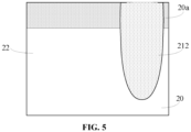
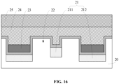
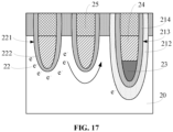
- FIGs. 4 to 17 are schematic cross-sectional structures corresponding to each step of a method for manufacturing a memory according to an example of the disclosure.
- schematic cross-sectional structures of the first cross-sectional direction AA and the second cross-sectional direction BB are provided for each of manufacturing steps.
- the substrate 20 includes an isolation structure 21 and an active area 22 located between adjacent isolation structures 21.
- the isolation structure 21 in the first cross-sectional direction AA, includes a first isolation structure 211 and a second isolation structure 212 with different widths.
- the width of the second isolation structure 212 is greater than that of the first isolation structure 211.
- the depth of the second isolation structure 212 in the substrate 20 is greater than that of the first isolation structure 211 in the substrate 20 due to an etch loading effect.
- “Etching loading effect” means that under the same etching process, the depth of the groove formed by etching is related to the width of the opening of at the top of the groove. The wider the opening at the top is, the more plasma gas acting on the etching is, so that the depth of the groove is deeper.
- a dielectric layer 20a is further provided at the top of the substrate 20, and can be used to protect the substrate 20 or to support other structures.
- the dielectric layer 20a is not shown in a schematic cross-sectional structure diagram in the first cross-sectional direction AA.
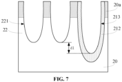
- an etching process is performed to form a first groove 213 in the isolation structure 21 and a second groove 221 in the active area 22.
- the depth of the first groove 213 in the substrate 20 is greater than that of the second groove 221 in the substrate 20, so that a thicker gate in the direction perpendicular to the surface of the substrate 20 can be formed by subsequent filling, thereby reducing the resistance of the word line in the second isolation structure 212.
- the depth of the first groove in the substrate is equal to or less than that of the second groove in the substrate.
- the first conductive layer subsequently filled at the bottom of the first groove 213 is staggered from the second gate subsequently filled in the second groove 221 in the direction perpendicular to the surface of the substrate 20, so that the presence of the first conductive layer does not affect the performance of the second gate.
- the depth of the first groove 213 in the substrate 20 is associated with the resistance of the first gate subsequently formed in the first groove 213 and the threshold voltage of the first gate structure.
- the first gate structure includes a first gate and a first gate dielectric layer. Where the thickness of the first gate dielectric layer is same, the deeper the depth of the first groove 213 is, the larger the cross-sectional area of the first gate subsequently formed is in the direction perpendicular to the substrate 20, so that the resistance of the first gate is less in the extending direction of the word line. In addition, where the same conductive material is filled, the deeper the depth of the first groove 213 is, the lager the size of the first gate is, the greater the intensity of the electric field of the first gate is, so that the threshold voltage of the first gate structure is lower.
- the first groove 213 has a first depth in the substrate 20, and the second groove 221 has a second depth in the substrate 20.
- the first depth difference d1 is 10% to 50%, for example, 20%, 30% or 40% of the depth of the first groove 213.
- the first depth difference d1 is too small, it is not advantageous to reduce the resistance of the word line in the second isolation structure 212, and it is prone for the first conductive layer subsequently formed to overlap with the front projection of the second gate filled in the second groove 221 in the direction parallel to the surface of the substrate, thereby affecting the performance of the second gate.
- the first depth difference d1 is too large, it is prone to cause etching defects due to the overlarge width-depth ratio.
- a third groove 215 is formed in the first isolation structure 211, and a first groove 213 is formed in the second isolation structure 212.
- the width of the opening of the third groove 215 is less than the width of the opening of the first groove 213 in the direction parallel to the surface of the substrate 20.
- the depth of the third groove 215 is less than that of the first groove 213 due to the etch loading effect.
- the threshold voltage of the gate structure in the third groove 215 is lower than that of the gate structure in the first groove 213, so that electrons of the active areas 22 at both sides of the second isolation structure 212 are prone to be actuated to gather in the channel region below the second isolation structure 212, thereby causing electronic transitions and signal interference.
- the gate in the second isolation structure 212 is adjusted to increase the gate threshold voltage, that is, the gate structure in the second isolation structure 212 is different from that in the first isolation structure 211, and only the first conductive layer is formed subsequently in the second isolation structure 212.
- the first conductive layer may also be filled in the third groove 215.
- the material of the gate structure in the third groove 215 is the same as that of the gate structure in the first groove 213.
- the gate structure in the first groove 213 is referred to as a first gate structure
- the gate structure in the active area 22 is referred to as a second gate structure
- the gate structure in the third groove 215 is referred to as a third gate structure.
- the material of the third gate structure is the same as that of the second gate structure.
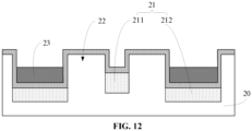
- a first gate dielectric layer 214 covering the bottom surface and sidewalls of the first groove 213 and a second gate dielectric layer 222 covering the bottom surface and sidewalls of the second groove 221 are formed.
- the first gate dielectric layer 214 and the second gate dielectric layer 222 are formed.
- the material of the first gate dielectric layer 214 is the same as that of the second gate dielectric layer 222.
- the first gate dielectric layer 214 is also located above the active area 22.
- the thickness of the first gate dielectric layer 214 is associated with the threshold voltage of the first gate structure and the resistance of the word line in the second isolation structure 212. Specifically, the thicker the first gate dielectric layer 214 is, the greater the isolation effect of the first gate dielectric layer 214 on the electric field of the first gate is. In addition, the first gate dielectric layer 214 is relatively thick, the reserved space of the first gate is less, the size of the first gate is smaller, the intensity of electric field of the first gate is less, and the threshold voltage of the first gate structure is higher. In addition, the less the size of the first gate is, the less the resistance of the word line in the second isolation structure 212 is.
- the first gate dielectric layer 214 can be provided so that its first thickness d2 in the direction perpendicular to the surface of the substrate 20 is thicker than its second thickness d3 in the direction parallel to the surface of the substrate 20.
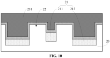
- a first deposition process is performed to form a first conductive layer 23 filled at the bottom of the first groove 213.
- the first deposition process includes the following acts.
- a first conductive film 231 filled up in the first groove 213 and the second groove 221 is formed.
- the first conductive film 231 is etched to form a first conductive layer 23 filled only at the bottom of the first groove 213.
- the work function of the material of the first conductive layer 23 is greater than that of the material of the second conductive layer subsequently formed.
- the material of the first conductive layer 23 includes at least one of titanium nitride, tungsten, nickel, or cobalt.
- the material of the first conductive layer 23 includes tungsten, and the crystal orientations of the tungsten of the first conductive layer 23 include [100] and [110]. It is noted that in the case that the material of the second conductive layer subsequently formed is also tungsten, the crystal orientation of the tungsten of the second conductive layer includes [111], [113] or [116], that is, the work function of the tungsten of the second conductive layer is less than that of the tungsten of the first conductive layer 23.
- the thickness of the first conductive layer 23 is in a range of 1 nm to 5 nm, for example, 2 nm, 3 nm, or 4 nm.
- the increase of the threshold voltage is less, so that the suppression of signal interference is weaker.
- the performance of the second gate structure in the active area 22 may be affected.
- a first blocking layer (not shown) covering the bottom surface and sidewalls of the first gate dielectric layer 214 and a second blocking layer (not shown) covering the bottom surface and sidewalls of the second gate dielectric layer 222 are also formed.
- the material of the first blocking layer may be the same as that of the second blocking layer.
- the blocking layer is configured to block the migration of metal ions in the gate towards the gate dielectric layer and the substrate 20.
- the first blocking layer and the second blocking layer may be formed in the same process.
- a second deposition process is performed to form a second conductive layer 24.
- the second conductive layer fills on the first conductive layer 23 and in the second groove 221.
- first conductive layer 23 and the second conductive layer 24 filled in the first groove 213 form a first gate; and the first gate and the first gate dielectric layer 214 form a first gate structure.
- the second conductive layer 24 filled in the second groove 221 forms a second gate; and the second gate and the second gate dielectric layer 222 form a second gate structure.
- an isolation layer 25 is formed.
- the isolation layer 25 is configured for electrical isolation.
- the material of the isolation layer 25 includes silicon nitride.
- the first gate further has a first conductive layer with a greater work function of material, so that the first gate structure has a higher threshold voltage than the second gate structure.
- the operating voltage applied to the first gate remains unchanged, as the threshold voltage of the first gate structure increases, the number of actuated electrons decreases, then the number of electrons gathered in the channel region below the isolation structure decreases, so that it is difficult to form the channel. In this way, it is difficult for the electrons to transition from one active area to another through the channel region, thereby reducing signal interference between the active areas at both sides of the isolation structure.
- an example of the disclosure further provides a memory which may be formed by the method for manufacturing a memory described above.
- the memory includes: a substrate 20 including an isolation structure 21 and an active area 22 located between adjacent isolation structures 21; a first gate structure (not shown) located in a first groove 213 in the isolation structure 21, in which the first gate structure includes a first gate (not shown) filled in the first groove 213, and the first gate includes a first conductive layer 23 filled at the bottom of the first groove 213 and a second conductive layer 24 located above the first conductive layer 23, and the work function of the material of the first conductive layer 23 is greater than that of the material of the second conductive layer 24; a second gate structure (not shown), in which the second gate structure is located in the second groove 221 of the active area 22, and the second gate structure includes a second gate (not shown) filled in the second groove 221, and the material of the second gate is the same as that of the second conductive layer.
- the first gate structure includes a first gate dielectric layer 214 covering the bottom surface and sidewalls of the first groove 213, and the second gate structure includes a second gate dielectric layer 222 covering the bottom surface and sidewalls of the second groove 221.
- the material of the first gate dielectric layer 214 is the same as that of the second gate dielectric layer 222.
- the depth of the first gate in the substrate 20 is greater than that of the second gate in the substrate 20.
- the isolation structure 21 further includes a third groove (not shown). In the direction parallel to the surface of the substrate 20, the width of the opening the first groove 213 is greater than that of the third groove.
- the third groove is filled with the third gate structure whose material is the same as that of the second gate structure.
- the top surface of the first conductive layer 23 is lower than or flush with the bottom surface of the second gate.
- the first gate structure further includes a first blocking layer located between the first gate and the first gate dielectric layer 214
- the second gate structure further includes a second blocking layer located between the second gate and the second gate dielectric layer 222.
- the material of the first blocking layer is the same as that of the second blocking layer.
- the thickness of the first conductive layer 23 is in a range of 1 nm to 5 nm, for example, 2 nm, 3 nm, or 4nm.
- the material of the first conductive layer 23 includes at least one of titanium nitride, tungsten, nickel or cobalt.
- the material of the first conductive layer 23 comprises tungsten, and the crystal orientations of the tungsten of the first conductive layer 23 include [100] and [110]. It is noted that in the case that the material of the second conductive layer subsequently formed is also tungsten, and the crystal orientation of the tungsten of the second conductive layer includes [111], [113] or [116], that is, the work function of the tungsten of the second conductive layer is less than that of the tungsten of the first conductive layer 23.
- the first gate further has a first conductive layer with a greater work function of material, so that the first gate structure has a higher threshold voltage than the second gate structure.
- the threshold voltage of the first gate structure increases, the number of electrons capable of being actuated by the operating voltage decreases, and the number of electrons gathered in the channel region below the isolation structure decreases, so that it is more difficult to form the channel. In this way, it is difficult for electrons to transition from one active area to another through the channel region, thereby reducing signal interference between the active areas at both sides of the second isolation structure.
Landscapes
- Engineering & Computer Science (AREA)
- Manufacturing & Machinery (AREA)
- Semiconductor Memories (AREA)
- Non-Volatile Memory (AREA)
Applications Claiming Priority (2)
| Application Number | Priority Date | Filing Date | Title |
|---|---|---|---|
| CN202010802218.4A CN114078849B (zh) | 2020-08-11 | 2020-08-11 | 存储器及其制作方法 |
| PCT/CN2020/138090 WO2022032957A1 (zh) | 2020-08-11 | 2020-12-21 | 存储器及其制作方法 |
Publications (2)
| Publication Number | Publication Date |
|---|---|
| EP4184580A1 true EP4184580A1 (de) | 2023-05-24 |
| EP4184580A4 EP4184580A4 (de) | 2024-01-17 |
Family
ID=80223206
Family Applications (1)
| Application Number | Title | Priority Date | Filing Date |
|---|---|---|---|
| EP20949449.1A Pending EP4184580A4 (de) | 2020-08-11 | 2020-12-21 | Speicher und herstellungsverfahren dafür |
Country Status (2)
| Country | Link |
|---|---|
| US (1) | US11864375B2 (de) |
| EP (1) | EP4184580A4 (de) |
Families Citing this family (1)
| Publication number | Priority date | Publication date | Assignee | Title |
|---|---|---|---|---|
| CN116113237B (zh) * | 2020-08-18 | 2024-11-15 | 长鑫存储技术有限公司 | 存储器及其制作方法 |
Family Cites Families (14)
| Publication number | Priority date | Publication date | Assignee | Title |
|---|---|---|---|---|
| US9117821B2 (en) * | 2013-03-12 | 2015-08-25 | Carnegie Mellon University | Oriented crystal nanowire interconnects |
| US9583615B2 (en) | 2015-02-17 | 2017-02-28 | Sandisk Technologies Llc | Vertical transistor and local interconnect structure |
| KR102741110B1 (ko) | 2017-01-26 | 2024-12-10 | 삼성전자주식회사 | 저항 구조체를 갖는 반도체 소자 |
| CN108807384B (zh) * | 2017-05-04 | 2019-10-18 | 联华电子股份有限公司 | 半导体元件及其制作方法 |
| CN107425072A (zh) * | 2017-09-06 | 2017-12-01 | 睿力集成电路有限公司 | 一种半导体存储器的器件结构 |
| KR102378471B1 (ko) * | 2017-09-18 | 2022-03-25 | 삼성전자주식회사 | 반도체 메모리 소자 및 그 제조 방법 |
| TWI629795B (zh) | 2017-09-29 | 2018-07-11 | Super Group Semiconductor Co., Ltd. | 溝槽式功率半導體元件及其製造方法 |
| KR102457515B1 (ko) | 2018-02-22 | 2022-10-21 | 에스케이하이닉스 주식회사 | 매립게이트구조를 구비한 반도체장치 및 그 제조 방법 |
| KR102552464B1 (ko) * | 2018-11-19 | 2023-07-06 | 삼성전자 주식회사 | 반도체 소자 |
| KR102731054B1 (ko) * | 2019-05-29 | 2024-11-15 | 삼성전자주식회사 | 집적회로 소자 및 그 제조 방법 |
| CN210245492U (zh) | 2019-07-02 | 2020-04-03 | 长鑫存储技术有限公司 | 半导体结构及存储器 |
| CN210156376U (zh) | 2019-08-30 | 2020-03-17 | 长鑫存储技术有限公司 | 半导体结构、存储装置 |
| CN110896053B (zh) | 2019-12-06 | 2022-04-29 | 绍兴中芯集成电路制造股份有限公司 | 屏蔽栅场效应晶体管及其形成方法 |
| KR102932515B1 (ko) * | 2020-08-07 | 2026-03-04 | 삼성전자주식회사 | 반도체 소자 및 그 제조방법 |
-
2020
- 2020-12-21 EP EP20949449.1A patent/EP4184580A4/de active Pending
-
2021
- 2021-07-12 US US17/372,893 patent/US11864375B2/en active Active
Also Published As
| Publication number | Publication date |
|---|---|
| US20220052051A1 (en) | 2022-02-17 |
| EP4184580A4 (de) | 2024-01-17 |
| US11864375B2 (en) | 2024-01-02 |
Similar Documents
| Publication | Publication Date | Title |
|---|---|---|
| US20160240538A1 (en) | Semiconductor device having buried gate, method of fabricating the same, and module and system having the same | |
| US12108587B2 (en) | Semiconductor device and method of forming same | |
| US20220302253A1 (en) | Manufacturing method of semiconductor structure and semiconductor structure | |
| US11818875B2 (en) | Methods for forming memory and memory | |
| WO2021185062A1 (zh) | 半导体结构及形成方法 | |
| US20220384615A1 (en) | Method for manufacturing metal gate | |
| US11864375B2 (en) | Memory and method for manufacturing same | |
| US20230411412A1 (en) | Semiconductor structure and forming method thereof | |
| CN114078849B (zh) | 存储器及其制作方法 | |
| US12513968B2 (en) | Semiconductor structure and method for manufacturing same | |
| CN115988870A (zh) | 半导体结构的制作方法及其结构 | |
| KR20110077503A (ko) | 플래시 메모리 소자의 플로팅 게이트 형성 방법 | |
| US20220367477A1 (en) | Semiconductor device and method for forming semiconductor device | |
| KR20040079171A (ko) | 반도체소자의 제조방법 | |
| KR100680966B1 (ko) | 반도체 소자의 게이트 형성방법 | |
| KR100509845B1 (ko) | 콘택 형성 방법 | |
| KR100780638B1 (ko) | 플래쉬 메모리 소자 및 그의 제조방법 | |
| KR20050122110A (ko) | 반도체 소자의 게이트 형성방법 | |
| KR20030001920A (ko) | 반도체 소자의 절연막 측벽 스페이서 형성 방법 | |
| CN114864477A (zh) | 半导体结构及其制造方法 | |
| KR20010052043A (ko) | 자기 정렬 컨택트와 랜딩 패드 구조를 갖는 반도체 장치및 그 형성 방법 | |
| KR19990070001A (ko) | 반도체 장치 커패시터의 제조 방법 | |
| KR20070089525A (ko) | 반도체 소자 제조 방법 | |
| KR19980022286A (ko) | 반도체 장치의 커패시터 제조 방법 | |
| KR20070032476A (ko) | 반도체 소자의 제조방법 |
Legal Events
| Date | Code | Title | Description |
|---|---|---|---|
| STAA | Information on the status of an ep patent application or granted ep patent |
Free format text: STATUS: THE INTERNATIONAL PUBLICATION HAS BEEN MADE |
|
| PUAI | Public reference made under article 153(3) epc to a published international application that has entered the european phase |
Free format text: ORIGINAL CODE: 0009012 |
|
| STAA | Information on the status of an ep patent application or granted ep patent |
Free format text: STATUS: REQUEST FOR EXAMINATION WAS MADE |
|
| 17P | Request for examination filed |
Effective date: 20230217 |
|
| AK | Designated contracting states |
Kind code of ref document: A1 Designated state(s): AL AT BE BG CH CY CZ DE DK EE ES FI FR GB GR HR HU IE IS IT LI LT LU LV MC MK MT NL NO PL PT RO RS SE SI SK SM TR |
|
| DAV | Request for validation of the european patent (deleted) | ||
| DAX | Request for extension of the european patent (deleted) | ||
| REG | Reference to a national code |
Ref country code: DE Ref legal event code: R079 Free format text: PREVIOUS MAIN CLASS: H01L0027108000 Ipc: H10B0012000000 |
|
| A4 | Supplementary search report drawn up and despatched |
Effective date: 20231215 |
|
| RIC1 | Information provided on ipc code assigned before grant |
Ipc: H10B 99/00 20230101ALI20231211BHEP Ipc: H01L 29/49 20060101ALI20231211BHEP Ipc: H01L 21/28 20060101ALI20231211BHEP Ipc: H01L 27/105 20230101ALI20231211BHEP Ipc: H01L 21/8234 20060101ALI20231211BHEP Ipc: H01L 29/423 20060101ALI20231211BHEP Ipc: H10B 12/00 20230101AFI20231211BHEP |
|
| STAA | Information on the status of an ep patent application or granted ep patent |
Free format text: STATUS: EXAMINATION IS IN PROGRESS |
|
| 17Q | First examination report despatched |
Effective date: 20250801 |