EP4145331A1 - Schablonenvermeidungsentwurfsverfahren und -vorrichtung sowie elektronische vorrichtung und speichermedium - Google Patents
Schablonenvermeidungsentwurfsverfahren und -vorrichtung sowie elektronische vorrichtung und speichermedium Download PDFInfo
- Publication number
- EP4145331A1 EP4145331A1 EP21868150.0A EP21868150A EP4145331A1 EP 4145331 A1 EP4145331 A1 EP 4145331A1 EP 21868150 A EP21868150 A EP 21868150A EP 4145331 A1 EP4145331 A1 EP 4145331A1
- Authority
- EP
- European Patent Office
- Prior art keywords
- stencil
- region
- stencil aperture
- aperture region
- area
- Prior art date
- Legal status (The legal status is an assumption and is not a legal conclusion. Google has not performed a legal analysis and makes no representation as to the accuracy of the status listed.)
- Pending
Links
Images


Classifications
-
- G—PHYSICS
- G06—COMPUTING OR CALCULATING; COUNTING
- G06F—ELECTRIC DIGITAL DATA PROCESSING
- G06F30/00—Computer-aided design [CAD]
- G06F30/30—Circuit design
- G06F30/39—Circuit design at the physical level
- G06F30/392—Floor-planning or layout, e.g. partitioning or placement
-
- G—PHYSICS
- G06—COMPUTING OR CALCULATING; COUNTING
- G06F—ELECTRIC DIGITAL DATA PROCESSING
- G06F30/00—Computer-aided design [CAD]
- G06F30/30—Circuit design
- G06F30/39—Circuit design at the physical level
- G06F30/398—Design verification or optimisation, e.g. using design rule check [DRC], layout versus schematics [LVS] or finite element methods [FEM]
-
- H—ELECTRICITY
- H05—ELECTRIC TECHNIQUES NOT OTHERWISE PROVIDED FOR
- H05K—PRINTED CIRCUITS; CASINGS OR CONSTRUCTIONAL DETAILS OF ELECTRIC APPARATUS; MANUFACTURE OF ASSEMBLAGES OF ELECTRICAL COMPONENTS
- H05K3/00—Apparatus or processes for manufacturing printed circuits
- H05K3/0005—Apparatus or processes for manufacturing printed circuits for designing circuits by computer
-
- H—ELECTRICITY
- H05—ELECTRIC TECHNIQUES NOT OTHERWISE PROVIDED FOR
- H05K—PRINTED CIRCUITS; CASINGS OR CONSTRUCTIONAL DETAILS OF ELECTRIC APPARATUS; MANUFACTURE OF ASSEMBLAGES OF ELECTRICAL COMPONENTS
- H05K3/00—Apparatus or processes for manufacturing printed circuits
- H05K3/10—Apparatus or processes for manufacturing printed circuits in which conductive material is applied to the insulating support in such a manner as to form the desired conductive pattern
- H05K3/12—Apparatus or processes for manufacturing printed circuits in which conductive material is applied to the insulating support in such a manner as to form the desired conductive pattern using thick film techniques, e.g. printing techniques to apply the conductive material or similar techniques for applying conductive paste or ink patterns
- H05K3/1216—Apparatus or processes for manufacturing printed circuits in which conductive material is applied to the insulating support in such a manner as to form the desired conductive pattern using thick film techniques, e.g. printing techniques to apply the conductive material or similar techniques for applying conductive paste or ink patterns by screen printing or stencil printing
- H05K3/1225—Screens or stencils; Holders therefor
-
- G—PHYSICS
- G06—COMPUTING OR CALCULATING; COUNTING
- G06F—ELECTRIC DIGITAL DATA PROCESSING
- G06F2115/00—Details relating to the type of the circuit
- G06F2115/12—Printed circuit boards [PCB] or multi-chip modules [MCM]
Definitions
- the present disclosure relates to the field of printed circuit boards, and in particular, to a stencil-avoidance design method, a stencil-avoidance design device, an electronic device and a non-transitory storage medium.
- stencil designs In current SMT processes, SMT defects caused by printing account for more than 60% of total defects. Among them, the defects caused by poor stencil designs, that is, unreasonable stencil aperture designs, account for more than 35% of total defects. Therefore, stencil designs play a crucial role in the quality and productivity of SMT. In stencil designs, it is necessary to design stencil apertures in such a way that they meet different requirements. In practice, when designing stencil apertures, certain distances between stencil apertures and other features including through-holes, solder resist regions, profiles (outer frames of the PCB), and device bodies of the PCB are needed so that the other features are able to "avoid” the stencil apertures; in other words, "avoidance" analysis of stencil apertures is needed in order to achieve the distances required by the SMT processes.
- the traditional manual avoidance method mainly has the following problems: 1) time-consuming (because it requires manually finding out stencil apertures that need modifications for avoidance purposes); 2) low coverage (because it cannot guarantee that the stencil apertures after modifications will satisfy the requirements of SMT processes); 3) easy to miss (because it cannot guarantee that all stencil apertures that need modifications for avoidance purposes will be found out by adopting the manual avoidance method.
- the above problems will affect the quality of stencil aperture designs, causing problems such as solder bridge, insufficient solder, exposed basis metal, non-wetting, and the like, which in turn affects the printing quality of PCBs.
- the present disclosure provides a stencil-avoidance design method, a stencil-avoidance design device, an electronic device and a non-transitory storage medium.
- the technical problems to be solved by the present disclosure is achieved through the following technical solutions:
- the present disclosure provides the stencil-avoidance design method, including:
- the step of obtaining the third region based on the second region includes: obtaining the third region through expanding or contracting the second region along a preset direction; wherein the preset direction is a direction pointing from the second region to the second stencil aperture region.
- the step of cropping the second stencil aperture region to obtain the third stencil aperture region includes: cropping off a collision portion of the second stencil aperture region to obtain the third stencil aperture region so that the third stencil aperture region does not collide with the third region.
- the first area ratio is a ratio of the area of the third stencil aperture region to an area of aperture walls corresponding to the third stencil region
- the second area ratio is a ratio of the area of the third stencil aperture region to the area of the second stencil aperture region.
- the step of obtaining a final stencil aperture region according to the first area ratio, the width-to-thickness ratio, the second area ratio, and the size ratio of the third stencil aperture region, and the relationship between the area of the third stencil aperture region and the area of the second stencil aperture region includes:
- the preset manner comprises at least one of a size adjustment manner, a position adjustment manner, and a shape adjustment manner.
- the step of processing the third stencil aperture region in the preset manner to obtain the graphically processed third stencil aperture region includes: processing the third stencil aperture region in the preset manner to obtain the graphically processed third stencil aperture region according to a preset order, where the size adjustment manner has a higher priority than the position adjustment manner, and the position adjustment manner has a higher priority than the shape adjustment manner.
- one of the first regions comprises at least one of a through-hole region, a solder resist region, a profile region, and a device body region.
- the present disclosure also provides the stencil-avoidance design device, including:
- the present disclosure also provides the electronic device, including: a processor, a communication interface, a memory and a communication bus, wherein the processor, the communication interface, and the memory are communicated with each other through the communication bus;
- the present disclosure also provides the non-transitory storage medium, the non-transitory storage medium stores a computer program, and the computer program implements the method described above when executed by the processor.
- the present disclosure determines the shortest distance between a selected element of multiple elements on the PCB and a selected stencil aperture of multiple stencil apertures, so as to obtain stencil apertures that need to be modified so that they do not collide with other elements. Collision tests are performed on the stencil apertures to be modified, before obtaining cropped stencil apertures. Finally, based on the first area ratio, the width-thickness ratio, the second area ratio, and the size ratio of the cropped stencil aperture and the relationship between the area of the third stencil aperture region and the area of the second stencil aperture region, it is determined whether the cropped stencil apertures need to be graphically processed, and then it is further determined whether the graphically processed stencil apertures meet the requirements according to the method of the present disclosure, until final stencil apertures are obtained.
- This method improves the efficiency, accuracy, coverage, and comprehensiveness of stencil aperture avoidance designs. It reduces manual intervention and avoid the problem of collision between elements due to human errors or omission of stencil apertures to be modified, as well as the problem of repeated modifications due to modified stencil apertures still not meeting process requirements.
- the method of the present disclosure has considerable advantages in terms of personnel requirements and operation methods, and replaces manual labor with automation, which is a trend in various industries.
- the present disclosure greatly reduces the design time of stencil apertures and improves the quality of stencil designs, which in turn improves the printing quality of PCBs.
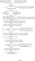
- a stencil-avoidance design method is provided in Embodiment 1, and the method includes the following steps:
- the first regions and the first stencil aperture regions are first obtained.
- the first regions are regions that may collide with some stencil apertures on a PCB, and the first stencil aperture regions are stencil aperture regions on a stencil. It is determined whether the shortest distance (i.e., a preset distance) between a selected first region of the plurality of first regions and a selected first stencil aperture region of the plurality of first stencil aperture regions is within the preset threshold range.
- the preset threshold range is a range in which the selected first stencil aperture region will need to be modified to better avoid the selected first region. If the shortest distance is not within the preset threshold range, the selected first stencil aperture region does not need to be modified, and the selected first stencil aperture region can be directly used as a final stencil aperture region.
- the selected first stencil aperture region needs to be modified to better avoid the selected first region, and the selected first region is used as the second region and the selected first stencil aperture region is used as the second stencil aperture region.
- the preset threshold range is for example, 0 to 0.2 mm; i.e., if the shortest distance is greater than 0 and less than 0.2 mm, the shortest distance is within the preset threshold range.
- the third stencil aperture region does not necessarily meet the requirements of final stencil aperture regions.
- the first area ratio is a ratio of the area of the third stencil aperture region to an area of aperture walls corresponding to the third stencil region
- the second area ratio is a ratio of the area of the third stencil aperture region to the area of the second stencil aperture region.
- the area of the third stencil aperture region is an area of the stencil aperture of the third stencil aperture region, the area of the aperture walls is the sum of areas of the aperture walls corresponding to the third stencil aperture region.
- the third stencil aperture region is the cropped second stencil aperture region.
- the smallest rectangle that can contain the third stencil aperture region is a first rectangle; the smallest rectangle that can contain the second stencil aperture region is a second rectangle; the width-to-thickness ratio is a ratio of the width of the first rectangle to the thickness of the third stencil aperture region; the size ratio is a ratio of the length of the first rectangle to the length of the second rectangle, or a ratio of the width of the first rectangle to the width of the second rectangle; the widths of the first, second rectangles are smaller than the lengths of the first, second rectangles.
- the first area ratio is the ratio of the area of the third stencil aperture region to the area of the aperture walls corresponding to the third stencil aperture region, wherein the aperture walls refers to walls of holes dug by the stencil.
- the width-to-thickness ratio is given by W1/D1, wherein W1 is the width of the first rectangle and D1 is the thickness of the third stencil aperture region.
- the second area ratio is the ratio of the area of the third stencil aperture region to the area of the second stencil aperture region, and the third stencil aperture region is the cropped second stencil aperture region.
- the size ratio is given by W1/W2, or L1/L2, wherein W1 is the width of the first rectangle, L1 is the length of the first rectangle, W2 is the width of the second rectangle, and L2 is the length of the second rectangle.
- one of the first regions includes at least one of a through-hole region, a solder resist region, a profile region, and a device body region.
- PCB design data is read and then preprocessed to obtain region data of the PCB, including data of through-holes, data of solder resist regions, data of profiles (i.e., outer frames of the PCB), data of device bodies, data of device coordinates and data of device package, etc.
- Data of solder paste layers is first generated based on the data of device package, the stencil aperture regions are created (or designed) for different types of devices based on the data of solder paste layers, and these stencil aperture regions are the first stencil aperture regions in one example. That is, the data of the stencil aperture regions used for avoidance analysis is hereby obtained.
- the Gerber file (whose filename extension is *.gbr) of the data of the stencil apertures is selected, and the stencil aperture layer is extracted by importing the Gerber file to obtain the first stencil aperture regions.
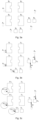
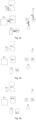
- the through-holes include through-holes A 1 , A 2 , A 3 , A 4 , and A 5
- the first stencil aperture regions include first stencil aperture regions B 1 , B 2 , B 3 , B 4 , B 5 , B 6 , B 7 , and B 8
- the distances between a selected through-hole (A 1 , A 2 , A 3 , A 4 , or As) and eight first stencil aperture regions (B 1 , B 2 , B 3 , B 4 , B 5 , B 6 , B 7 , and B 8 ) are measured respectively, and the shortest distance between the selected through-hole (A 1 , A 2 , A 3 , A 4 , or A 5 ) and eight first stencil aperture regions is determined from the distances.
- the distance between a selected through-hole and the first stencil aperture region closest to the selected through-hole is noted as an AB spacing (d1, d2, d3, d4, d5, for example), if the AB spacing is greater than 0 and less than 0.2 mm, the distance between the selected through-hole and the corresponding first stencil aperture region is within the preset threshold range.
- d1, d2, and d3 are all within the preset threshold range, the through-hole A 1 and the first stencil aperture region B 1 , the through-hole A 2 and the first stencil aperture region B 3 , and the through-hole As and the first stencil aperture region B 5 are regions that satisfy the preset threshold range. As shown in FIG.
- the through-hole A 1 , the through-hole A 2 , the through-hole A 3 , the first stencil aperture region B 1 , the first stencil aperture region B 3 and the first stencil aperture region B 5 are then recorded as through-hole A 11, through-hole A1 2 , through-hole A1 3 and first stencil aperture region B 11, first stencil aperture region B1 3 and first stencil aperture region B1 5 , respectively.
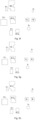
- step 1.3 may include: obtaining the third region through expanding or contracting the second region along a preset direction, wherein the preset direction is a direction pointing from the second region to the second stencil aperture region.
- the second region is expanded or contracted along a direction pointing from the second region to the second stencil aperture region, and the expanded or contracted second region is used as the third region.
- the second region is a through-hole region, a solder resist region, or a device body region
- the second region is expanded, and when the second region is a profile region, the second region is contracted.
- the through-hole A1 1 , the through-hole A1 2 , and the through-hole A1 3 need to be expanded, for example, a specified distance is added to the original radius of each through-hole to obtain an expanded through-hole A1 1 , an expanded through-hole A1 2 , and an expanded through-hole A1 3 ; for example, if the specified distance is 0.2 mm and the original radius of a through-hole is 0.1 mm, the radius of the corresponding expanded through-hole is 0.3 mm.
- the specified distance is any value within the preset threshold range.
- step 1.4 includes: determining whether the third region collides with the second stencil aperture region, and cropping the second stencil aperture region to obtain a third stencil aperture region if the third region collides with the second stencil aperture region.
- the third region and the second stencil aperture region are subjected to a collision test. If the third region collides with the second stencil aperture region, the portion of the second stencil aperture region that overlaps with the third region is defined as a collision portion, which is then cropped off and the cropped second stencil aperture region is used as the third stencil aperture region so that the third stencil aperture region does not collide with the third region.
- the first stencil aperture region B2 1 is a region obtained from cropping the first stencil aperture region B1 1
- the first stencil aperture region B2s is a region obtained from cropping the first stencil aperture region B1 3
- the first stencil aperture region B2 5 is a region obtained from cropping the first stencil aperture region B1 5 .
- the respective notched portion of the first stencil aperture regions B2 1 , B2s, and B2s in FIG. 3d is where cropping takes place.
- step 1.5 includes the following steps:
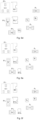
- a selected third stencil aperture region when a selected third stencil aperture region satisfies the first condition, the second condition, and the third condition, it means that the distances between the selected third stencil aperture region and the regions on the PCB all satisfy the distance requirement and modification for avoidance purposes is not required, and then the selected third stencil aperture region replaces the initially designed first stencil aperture region and is used as a final stencil aperture region. If any one of the first condition, the second condition, and the third condition is not satisfied, it means that a distance between the selected third stencil aperture region and one region on the PCB does not satisfy the distance requirement and modification for avoidance purposes is required, and then the selected third stencil aperture region may be adjusted in the preset manner, such as adjusting the size, shape or position of the selected third stencil aperture region.
- the first threshold is 0.66
- the second threshold is 1.5
- the third threshold is 20%
- the fourth threshold is 50%
- a fifth threshold is 50%.
- the first area ratio is greater than 0.66
- the width-to-thickness ratio is greater than 1.5
- the second area ratio is greater than 50%
- the size ratio is greater than 50%
- the ratio of the area of the third stencil aperture region to the area of the second stencil aperture region is less than 20%.
- the preset manner includes at least one of a size adjustment manner, a position adjustment manner, and a shape adjustment manner. If the third stencil aperture region does not satisfy the first condition, the second condition, and the third condition, the third stencil aperture region can be adjusted by the size adjustment manner and/or the position adjustment manner and/or the shape adjustment manner.
- the size adjustment manner can be performed by reducing the size of the third stencil aperture region, for example, reducing the overall size of the third stencil aperture region by 20 times (i.e., the shrunk third stencil aperture region is 0.05 times as large as the original one), the position adjustment manner can be performed by moving the third stencil aperture region away from the regions to be avoided, and the shape adjustment manner can be performed by adjusting the width or length of the third stencil aperture region.
- the step of processing the third stencil aperture region in the preset manner to obtain a graphically processed third stencil aperture region includes: processing the third stencil aperture region in the preset manner to obtain the graphically processed third stencil aperture region according to a preset order, where the size adjustment manner has a higher priority than the position adjustment manner, and the position adjustment manner has a higher priority than the shape adjustment manner.
- the third stencil aperture region is adjusted only by the size adjustment manner, or only by the position adjustment manner, or only by the shape adjustment manner, or by two adjustment manners or three adjustment manners as described above.
- the adjustment manners can be selected in a preset order. For example, when only one adjustment manner is used, the size adjustment manner has a higher priority than the position adjustment manner, and the position adjustment manner has a higher priority than the shape adjustment manner. When two adjustment manners are used, the priority of a combination of the size adjustment manner and the position adjustment manner where the size adjustment manner is used before the position adjustment method is higher than that of a combination of the position adjustment manner and the shape adjustment manner where the position adjustment manner is used before the shape adjustment method. When three adjustment manners are used, the size adjustment manner is first used, then the position adjustment method is used, and the shape adjustment method is last used.
- the third stencil aperture region B2s, B2 5 in FIG. 3d satisfy the first condition, the second condition, and the third condition
- the third stencil aperture region B2s replaces the first stencil aperture region B 3
- the third stencil aperture region B2 5 replaces the first stencil aperture region B 5
- the third stencil aperture regions B2s, B2 5 are used as new stencil aperture regions, such as, B12 3 , B12 5 in FIG. 3e .
- the third stencil aperture region B2 1 needs to be modified.
- the third stencil aperture region B2 1 is first modified (e.g., reduced by 5%), then the position of the third stencil aperture region B2 1 is modified (e.g., the third stencil aperture region B2 1 moves for a specified distance in a direction pointing from the through-hole A 11 to the third stencil aperture region B2 1 , and the specified distance is, for example, 0.001 mm), and then the shape of the third stencil aperture B2 1 is modified (e.g., the length and/or width of the third stencil aperture B2 1 is adjusted minutely, for example, a ratio of the adjustment(to the original dimension (length or width) is within a threshold range, e.g., 0.5%-10%) to generate a new stencil aperture region B3 1 shown in FIG. 3f .
- a ratio of the adjustment(to the original dimension (length or width) is within a threshold range, e.g., 0.5%-10%) to generate a new stencil aperture region B3 1 shown in FIG. 3f .
- the stencil aperture region B3 1 is obtained by moving the third stencil aperture region B2 1 for the specified distance in the direction pointing from the through-hole A 11 to the third stencil aperture region B2 1 , and increasing the width of the third stencil aperture region B2 1 so that the ratio of the increase to the original width meets the threshold range (e.g., 0.5%-10%).
- Step 1.53 performing step 1.51 and step 1.52 on the graphically processed third stencil aperture region, after which graphical processing is performed for N times on the third stencil aperture region and/or the graphically processed third stencil aperture region, wherein a final stencil aperture region is obtained based on the third stencil aperture region graphical if N is not greater than a preset threshold and the third stencil aperture region after N times of graphical processing satisfies the first condition, the second condition, and the third condition; wherein a fourth stencil aperture region is obtained if the N is equal to the preset threshold and the third stencil aperture regions after N times of graphical processing does not satisfy all of the first condition, the second condition, and the third condition, wherein N is a positive integer.
- steps 1.51 to 1.52 are performed on the graphically processed third stencil aperture region, after which graphical processing is performed for N times on the third stencil aperture region and/or the graphically processed third stencil aperture region. If N is less than or equal to the preset threshold and the third stencil aperture region after N times of graphical processing satisfies the first condition, the second condition, and the third condition, the third stencil aperture region after N times of graphical processing replaces the original stencil aperture region to be used as the final stencil aperture region.
- N is equal to the preset threshold and the third stencil aperture region after N times of graphical processing does not satisfy the first condition, the second condition, and the third condition at the same time, it means that the third stencil aperture region after N times of graphical processing still does not meet the requirements after the above adjustment manners, and the third stencil aperture region after N times of graphical processing is used as the fourth stencil aperture region.
- the stencil aperture region Bi1 is the stencil aperture region after i times of graphical processing.
- the preset threshold is, for example, 20.
- the final stencil aperture region obtained after i times of graphical processing (e.g., B 1 i1) is represented in FIG. 3h .
- Step 1.54 modifying the fourth stencil aperture region to obtain the final stencil aperture region.
- the fourth stencil aperture regions that do not meet the requirements are counted one by one, returned to the window for the avoidance analysis in the form of a report, and their corresponding coordinate positions are displayed for manual reviewing and modification, and the fourth stencil aperture regions that do not meet the requirements are manually modified to obtain the final stencil aperture regions that meet the design requirements.
- this embodiment modifies the first regions to be the third region only for determining whether the stencil aperture region needs to be modified, and after the final stencil aperture region is determined using the method of the present disclosure, the through-holes, solder resist regions, profile regions, and device bodies should stay unchanged.
- the present disclosure determines the shortest distance between a selected element of multiple elements on the PCB and a selected stencil aperture of multiple stencil apertures, so as to obtain stencil apertures that need to be modified so that they do not collide with other elements. Collision tests are performed on the stencil apertures to be modified, before obtaining cropped stencil apertures. Finally, based on the first area ratio, the width-thickness ratio, the second area ratio, the size ratio of the cropped stencil aperture and the relationship between the area of the third stencil aperture region and the area of the second stencil aperture region, it is determined whether the cropped stencil apertures need to be graphically processed, and then it is further determined whether the graphically processed stencil apertures meet the requirements according to the method of the present disclosure, until final stencil apertures are obtained.
- This method improves the efficiency, accuracy, coverage, and comprehensiveness of stencil aperture avoidance designs. It reduces manual intervention and avoid the problem of collision between elements due to human errors or omission of stencil apertures to be modified, as well as the problem of repeated modifications due to modified stencil apertures still not meeting process requirements.
- the method of the present disclosure has considerable advantages in terms of personnel requirements and operation methods, and replaces manual labor with automation, which is a trend in various industries.
- the present disclosure greatly reduces the design time of stencil apertures and improves the quality of stencil designs, which in turn improves the printing quality of PCBs.
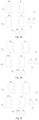
- FIGs. 4a-4h are schematic diagrams of a process of a stencil-avoidance design method involving profiles according to an embodiment of the present disclosure.
- this embodiment takes the first regions being the profile of the PCB as an example to illustrate the process.
- the process includes the following steps:
- FIGs. 5a-5h are schematic diagrams of the stencil-avoidance design method involving solder resists according to an embodiment of the present disclosure.
- this embodiment takes the first regions being the solder resists as an example to illustrate the process.
- the process includes the following steps:
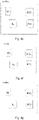
- FIGs. 6a-6h are schematic diagrams of the stencil-avoidance design method involving device bodies according to an embodiment of the present disclosure.
- the embodiment takes the first regions being the device bodies as an example to illustrate the process.
- the process specifically includes the following steps:
- FIG. 7 is a schematic structural diagram of a stencil-avoidance design device according to an embodiment of the present disclosure.
- the stencil-avoidance design device includes an acquisition module, a first analysis module, a region processing module, a second analysis module, and a detection module.
- the acquisition module is used to obtain a plurality of first regions and a plurality of first stencil aperture regions.
- the first analysis module is used to determine whether a shortest distance between a selected first region of the plurality of first regions and a selected first stencil aperture region f the plurality of first stencil aperture regions is within a preset threshold range, and use the selected first region as a second region and use the selected first stencil aperture region as a second stencil aperture region if the shortest distance is within the preset threshold range.
- the region processing module is used to obtain a third region based on the second region; wherein a collision test is performed on the third region and with the second stencil aperture region.
- the second analysis module is used to determine whether the third region collides with the second stencil aperture region, and cropping the second stencil aperture region to obtain a third stencil aperture region if the third region collides with the second stencil aperture region.
- the detection module is used to obtain a final stencil aperture region according to a first area ratio, a width-to-thickness ratio, a second area ratio, and a size ratio of the third stencil aperture region, and a relationship between an area of the third stencil aperture region and an area of the second stencil aperture region.
- This embodiment provides the stencil-avoidance design device that can perform the methods described above with similar implementation principles and technical effects.
- FIG. 8 is a schematic structural diagram of an electronic device according to an embodiment of the present disclosure.
- the electronic device 1100 includes a processor 1101, a communication interface 1102, a memory 1103, and a communication bus 1104.
- the processor 1101, the communication interface 1102, and the memory 1103 are communicated with each other through the communication bus 1104.
- the memory 1103 is used to store a computer program.
- the processor 1101 is used to implement the method described above when executing the computer program.
- the processor 1101 implements the following steps when executing the computer program.
- Step 1.1 obtaining a plurality of first regions and a plurality of first stencil aperture regions.
- Step 1.2 determining whether a shortest distance between a selected first region of the plurality of first regions and a selected first stencil aperture region of the plurality of first stencil aperture regions is within a preset threshold range, and using the selected first region as a second region and using the selected first stencil aperture region as a second stencil aperture region if the shortest distance is within the preset threshold range.
- Step 1.3 obtaining a third region based on the second region, wherein a collision test is performed on the third region and the second stencil aperture region.
- Step 1.4 determining whether the third region collides with the second stencil aperture region, and cropping the second stencil aperture region to obtain a third stencil aperture region if the third region collides with the second stencil aperture region.
- Step 1.5 obtaining a final stencil aperture region according to a first area ratio, a width-to-thickness ratio, a second area ratio, and a size ratio of the third stencil aperture region, and a relationship between an area of the third stencil aperture region and an area of the second stencil aperture region.
- the present embodiment provides the electronic device that can perform the methods described above with similar implementation principles and technical effects.
- the present embodiment provides a computer readable storage medium; the computer readable storage medium stores a computer program, and the computer program implements the method described above when executed by the processor:
- the present embodiment provides the computer readable storage medium that can perform the methods described above with similar implementation principles and technical effects.
- embodiments of the present disclosure may be provided as methods, devices (apparatus), or computer program products. Accordingly, the present disclosure may adopt an entirely hardware embodiment, an entirely software embodiment, or an embodiment combining software and hardware, all of which are collectively referred to herein as a "module” or “system”. Further, the present disclosure may adopt computer program products implemented on one or more computer-readable storage medium (including, but not limited to, disk memory, CD-ROM, optical memory, etc.) that stores the computer-usable program code.
- the computer program is stored/distributed in a suitable medium, provided with or as part of other hardware, and may also take other forms of distribution, such as via the Internet or other wired or wireless telecommunications systems.
- first and second are used for descriptive purposes only and can not be understood as indicating or implying relative importance or implicitly specifying the number of technical features indicated. Thus, the features qualified with “first” and “second” may explicitly or implicitly include one or more such features.
- “plurality” means two or more, unless otherwise expressly and specifically limited.
Landscapes
- Engineering & Computer Science (AREA)
- Computer Hardware Design (AREA)
- Theoretical Computer Science (AREA)
- Physics & Mathematics (AREA)
- General Engineering & Computer Science (AREA)
- Geometry (AREA)
- Evolutionary Computation (AREA)
- General Physics & Mathematics (AREA)
- Manufacturing & Machinery (AREA)
- Microelectronics & Electronic Packaging (AREA)
- Architecture (AREA)
- Electric Connection Of Electric Components To Printed Circuits (AREA)
- Manufacture Or Reproduction Of Printing Formes (AREA)
- Printing Plates And Materials Therefor (AREA)
Applications Claiming Priority (2)
| Application Number | Priority Date | Filing Date | Title |
|---|---|---|---|
| CN202010974513.8A CN112232014B (zh) | 2020-09-16 | 2020-09-16 | 钢网避让设计方法、设计装置、电子设备及存储介质 |
| PCT/CN2021/097211 WO2022057313A1 (zh) | 2020-09-16 | 2021-05-31 | 钢网避让设计方法、设计装置、电子设备及存储介质 |
Publications (2)
| Publication Number | Publication Date |
|---|---|
| EP4145331A1 true EP4145331A1 (de) | 2023-03-08 |
| EP4145331A4 EP4145331A4 (de) | 2024-06-05 |
Family
ID=74106955
Family Applications (1)
| Application Number | Title | Priority Date | Filing Date |
|---|---|---|---|
| EP21868150.0A Pending EP4145331A4 (de) | 2020-09-16 | 2021-05-31 | Schablonenvermeidungsentwurfsverfahren und -vorrichtung sowie elektronische vorrichtung und speichermedium |
Country Status (5)
| Country | Link |
|---|---|
| US (1) | US11775731B2 (de) |
| EP (1) | EP4145331A4 (de) |
| JP (1) | JP7479616B2 (de) |
| CN (1) | CN112232014B (de) |
| WO (1) | WO2022057313A1 (de) |
Families Citing this family (4)
| Publication number | Priority date | Publication date | Assignee | Title |
|---|---|---|---|---|
| CN112232014B (zh) * | 2020-09-16 | 2022-07-29 | 上海望友信息科技有限公司 | 钢网避让设计方法、设计装置、电子设备及存储介质 |
| CN112788859B (zh) * | 2021-01-21 | 2022-04-01 | 上海望友信息科技有限公司 | 一种屏蔽框钢网开口方法、装置、电子设备及存储介质 |
| PH12022050163A1 (en) * | 2021-05-18 | 2023-04-17 | Inari Tech Sdn Bhd | Apparatus, system and method for determining a match condition for a printed circuit board to a stencil |
| CN115408975B (zh) * | 2022-09-21 | 2025-08-12 | 上海望友信息科技有限公司 | 一种微改版钢网设计的方法、系统、电子设备及存储介质 |
Family Cites Families (13)
| Publication number | Priority date | Publication date | Assignee | Title |
|---|---|---|---|---|
| US6938227B2 (en) * | 2002-08-08 | 2005-08-30 | Fry's Metals, Inc. | System and method for modifying electronic design data |
| JP2004334302A (ja) * | 2003-04-30 | 2004-11-25 | Ngk Spark Plug Co Ltd | 電子回路基板用camデータ作成方法、電子回路基板用cad/camシステムとそれに使用するコンピュータプログラム、及び電子回路基板の製造方法 |
| JP2005228999A (ja) * | 2004-02-13 | 2005-08-25 | Sharp Corp | 半導体集積回路のレイアウトパターン修正装置、半導体集積回路のレイアウトパターン修正方法、半導体集積装置の製造方法、半導体集積回路のレイアウトパターン修正プログラムおよび可読記録媒体 |
| JP2007265179A (ja) * | 2006-03-29 | 2007-10-11 | Fujitsu Ltd | レイアウト検証方法、レイアウト検証装置 |
| JP5606932B2 (ja) * | 2011-01-18 | 2014-10-15 | ルネサスエレクトロニクス株式会社 | マスクの製造方法ならびに光近接効果補正の補正方法および半導体装置の製造方法 |
| CN106227946B (zh) * | 2016-07-26 | 2019-03-12 | 上海望友信息科技有限公司 | 一种pcb网板制作方法及系统 |
| CN108829907A (zh) * | 2018-04-11 | 2018-11-16 | 上海望友信息科技有限公司 | 基于eda封装库创建钢网库的方法及系统、存储介质及终端 |
| US10785867B2 (en) * | 2018-09-25 | 2020-09-22 | International Business Machines Corporation | Automatic determination of power plane shape in printed circuit board |
| CN109977518B (zh) * | 2019-03-19 | 2021-02-12 | 上海望友信息科技有限公司 | 网板阶梯的设计方法、系统、计算机可读存储介质及设备 |
| CN110600402B (zh) * | 2019-08-27 | 2022-05-13 | 上海望友信息科技有限公司 | 钢网开口的设计方法、钢网开口的设计装置及电子设备 |
| CN111191408A (zh) * | 2019-12-26 | 2020-05-22 | 深圳市元征科技股份有限公司 | 一种pcb元件布局校验方法、装置、服务器及存储介质 |
| CN111291530B (zh) * | 2020-02-23 | 2022-08-12 | 苏州浪潮智能科技有限公司 | 一种pcb板中避免走线与阻焊层重叠的方法及系统 |
| CN112232014B (zh) * | 2020-09-16 | 2022-07-29 | 上海望友信息科技有限公司 | 钢网避让设计方法、设计装置、电子设备及存储介质 |
-
2020
- 2020-09-16 CN CN202010974513.8A patent/CN112232014B/zh active Active
-
2021
- 2021-05-31 JP JP2022567149A patent/JP7479616B2/ja active Active
- 2021-05-31 WO PCT/CN2021/097211 patent/WO2022057313A1/zh not_active Ceased
- 2021-05-31 EP EP21868150.0A patent/EP4145331A4/de active Pending
- 2021-05-31 US US18/009,804 patent/US11775731B2/en active Active
Also Published As
| Publication number | Publication date |
|---|---|
| JP2023524120A (ja) | 2023-06-08 |
| JP7479616B2 (ja) | 2024-05-09 |
| EP4145331A4 (de) | 2024-06-05 |
| CN112232014B (zh) | 2022-07-29 |
| US11775731B2 (en) | 2023-10-03 |
| CN112232014A (zh) | 2021-01-15 |
| US20230205973A1 (en) | 2023-06-29 |
| WO2022057313A1 (zh) | 2022-03-24 |
Similar Documents
| Publication | Publication Date | Title |
|---|---|---|
| EP4145331A1 (de) | Schablonenvermeidungsentwurfsverfahren und -vorrichtung sowie elektronische vorrichtung und speichermedium | |
| DE19609652B4 (de) | Verfahren und Vorrichtung zur Korrektur von Maskenmustern | |
| CN108009316B (zh) | Opc修正方法 | |
| DE2722567A1 (de) | Lageerkennungssystem | |
| DE102008050836A1 (de) | Vorrichtung zum Überprüfen von im Druckverfahren aufgebrachtem Lot | |
| US10061209B2 (en) | Method for verifying a pattern of features printed by a lithography process | |
| CN110929470A (zh) | 版图优化方法 | |
| CN111103768B (zh) | 一种减少晶圆边缘聚焦不良的方法 | |
| DE102007042272A1 (de) | Verfahren zur Korrektur der durch Lensdistortion eines Objektivs verursachten Messfehler | |
| CN101290904A (zh) | 修正接触孔金属覆盖层布图设计的方法 | |
| CN119540196A (zh) | 一种光罩缺陷识别方法 | |
| DE10304674B4 (de) | Verfahren zum Belichten eines Substrates mit einem den optischen Proximity-Effekt ausgleichenden Strukturmuster | |
| CN109271665B (zh) | 一种自动确定标注参数的方法及装置 | |
| CN111948900B (zh) | 版图的特征图形的识别方法 | |
| US12100147B2 (en) | Method for fitting image | |
| CN114828418B (zh) | 一种pcb自动移线处理的方法 | |
| CN112949242B (zh) | 遮光带版图绘制方法、光罩版图绘制方法及光罩版图 | |
| DE102006003422A1 (de) | Muster-Festlegungsverfahren und Muster-Festlegungsvorrichtung | |
| CN118380344B (zh) | 晶圆重复缺陷检测方法、装置、电子装置和存储介质 | |
| CN112739044A (zh) | 一种自动化脚本制作防焊测试线的方法 | |
| US11977335B2 (en) | Pattern decomposition method | |
| CN117853558A (zh) | 一种电路板中的绿油桥区域提取方法、装置及系统 | |
| JPH07148907A (ja) | 画像認識位置合わせ方法及びその装置 | |
| DE68919888T2 (de) | Bildverarbeitungsmethode. | |
| US6523164B2 (en) | Method and apparatus for modifying flattened data of designed circuit pattern |
Legal Events
| Date | Code | Title | Description |
|---|---|---|---|
| STAA | Information on the status of an ep patent application or granted ep patent |
Free format text: STATUS: THE INTERNATIONAL PUBLICATION HAS BEEN MADE |
|
| PUAI | Public reference made under article 153(3) epc to a published international application that has entered the european phase |
Free format text: ORIGINAL CODE: 0009012 |
|
| STAA | Information on the status of an ep patent application or granted ep patent |
Free format text: STATUS: REQUEST FOR EXAMINATION WAS MADE |
|
| 17P | Request for examination filed |
Effective date: 20221129 |
|
| AK | Designated contracting states |
Kind code of ref document: A1 Designated state(s): AL AT BE BG CH CY CZ DE DK EE ES FI FR GB GR HR HU IE IS IT LI LT LU LV MC MK MT NL NO PL PT RO RS SE SI SK SM TR |
|
| DAV | Request for validation of the european patent (deleted) | ||
| DAX | Request for extension of the european patent (deleted) | ||
| A4 | Supplementary search report drawn up and despatched |
Effective date: 20240503 |
|
| RIC1 | Information provided on ipc code assigned before grant |
Ipc: G06F 115/12 20200101ALI20240427BHEP Ipc: G06F 30/392 20200101AFI20240427BHEP |