EP4124181A1 - Hochfrequenz-leistungsversorgungsvorrichtung und ausgangssteuerungsverfahren dafür - Google Patents
Hochfrequenz-leistungsversorgungsvorrichtung und ausgangssteuerungsverfahren dafür Download PDFInfo
- Publication number
- EP4124181A1 EP4124181A1 EP21771286.8A EP21771286A EP4124181A1 EP 4124181 A1 EP4124181 A1 EP 4124181A1 EP 21771286 A EP21771286 A EP 21771286A EP 4124181 A1 EP4124181 A1 EP 4124181A1
- Authority
- EP
- European Patent Office
- Prior art keywords
- output
- level
- signal
- pulse
- level setting
- Prior art date
- Legal status (The legal status is an assumption and is not a legal conclusion. Google has not performed a legal analysis and makes no representation as to the accuracy of the status listed.)
- Pending
Links
Images


Classifications
-
- H—ELECTRICITY
- H01—ELECTRIC ELEMENTS
- H01J—ELECTRIC DISCHARGE TUBES OR DISCHARGE LAMPS
- H01J37/00—Discharge tubes with provision for introducing objects or material to be exposed to the discharge, e.g. for the purpose of examination or processing thereof
- H01J37/32—Gas-filled discharge tubes
- H01J37/32009—Arrangements for generation of plasma specially adapted for examination or treatment of objects, e.g. plasma sources
- H01J37/32082—Radio frequency generated discharge
- H01J37/32137—Radio frequency generated discharge controlling of the discharge by modulation of energy
- H01J37/32146—Amplitude modulation, includes pulsing
-
- H—ELECTRICITY
- H01—ELECTRIC ELEMENTS
- H01J—ELECTRIC DISCHARGE TUBES OR DISCHARGE LAMPS
- H01J37/00—Discharge tubes with provision for introducing objects or material to be exposed to the discharge, e.g. for the purpose of examination or processing thereof
- H01J37/32—Gas-filled discharge tubes
- H01J37/32009—Arrangements for generation of plasma specially adapted for examination or treatment of objects, e.g. plasma sources
- H01J37/32082—Radio frequency generated discharge
- H01J37/32137—Radio frequency generated discharge controlling of the discharge by modulation of energy
- H01J37/32155—Frequency modulation
- H01J37/32165—Plural frequencies
-
- H—ELECTRICITY
- H01—ELECTRIC ELEMENTS
- H01J—ELECTRIC DISCHARGE TUBES OR DISCHARGE LAMPS
- H01J37/00—Discharge tubes with provision for introducing objects or material to be exposed to the discharge, e.g. for the purpose of examination or processing thereof
- H01J37/32—Gas-filled discharge tubes
- H01J37/32009—Arrangements for generation of plasma specially adapted for examination or treatment of objects, e.g. plasma sources
- H01J37/32082—Radio frequency generated discharge
- H01J37/32174—Circuits specially adapted for controlling the RF discharge
-
- H—ELECTRICITY
- H01—ELECTRIC ELEMENTS
- H01J—ELECTRIC DISCHARGE TUBES OR DISCHARGE LAMPS
- H01J2237/00—Discharge tubes exposing object to beam, e.g. for analysis treatment, etching, imaging
- H01J2237/32—Processing objects by plasma generation
- H01J2237/327—Arrangements for generating the plasma
-
- H—ELECTRICITY
- H01—ELECTRIC ELEMENTS
- H01J—ELECTRIC DISCHARGE TUBES OR DISCHARGE LAMPS
- H01J2237/00—Discharge tubes exposing object to beam, e.g. for analysis treatment, etching, imaging
- H01J2237/32—Processing objects by plasma generation
- H01J2237/33—Processing objects by plasma generation characterised by the type of processing
- H01J2237/334—Etching
-
- H—ELECTRICITY
- H05—ELECTRIC TECHNIQUES NOT OTHERWISE PROVIDED FOR
- H05H—PLASMA TECHNIQUE; PRODUCTION OF ACCELERATED ELECTRICALLY-CHARGED PARTICLES OR OF NEUTRONS; PRODUCTION OR ACCELERATION OF NEUTRAL MOLECULAR OR ATOMIC BEAMS
- H05H2242/00—Auxiliary systems
- H05H2242/20—Power circuits
- H05H2242/22—DC, AC or pulsed generators
Definitions
- the present invention relates to a high-frequency power supply device to be applied to a plasma generation device and others, in particular a high-frequency power supply device for outputting a high-frequency pulse to a target device based on a synchronous pulse and a clock pulse, and to an output control method therefor.
- a high-frequency power supply device is applied as a power source for ultrasonic oscillation, generation of induced power, plasma generation or others, and is a power supply device that combines a synchronous pulse for determining an output period of a high-frequency pulse and a clock pulse for determining a pulse period of a high-frequency component to be oscillated, thereby enabling to output a high-frequency pulse containing a high-frequency component over a predetermined period with a predetermined amplitude value.
- a switch-type high-frequency power supply device that has amplitude values respectively at a high level (first level) and a low level (second level) in one oscillation period.
- Patent Literature 1 discloses a plasma etching device that has a processing chamber filled with etching gas and accommodating a semiconductor wafer to be processed, in which an upper electrode and a lower electrode are disposed to face each other with the wafer to be processed being held between them, and a high-frequency voltage from a high-frequency power source is applied to the upper electrode and the lower electrode to cause electrical discharge between the upper electrode and the lower electrode so as to turn the etching gas into plasma, thereby performing etching process on the wafer to be processed.
- a voltage applied from the high-frequency power source is stable.
- Patent Literature 2 discloses a technique of feedback control, in which a matching network is connected between a high-frequency generator and a plasma processing chamber for converting a complex impedance of plasma viewed from an end of a transmission path into a nominal impedance of the high-frequency generator, so as to perform the feedback control on a voltage of an induction coil for feeding high-frequency power to the plasma processing chamber.
- the matching network allows the feedback control to match phases of electric power waveforms applied to the induction coil to thereby stabilize substrate treatment.
- a synchronous pulse generator for generating a synchronous pulse and a clock pulse generator for generating a clock pulse are typically provided separately, and since these generators operate independently, it is inevitable that phases of output waveforms generated based on clock pulses in high-frequency pulses output at timings based on the synchronous pulses are uneven at the time of changing output levels of the high-frequency pulses.
- the number of pulses due to an amplitude at a first level and the number of pulses due to an amplitude at a second level are different from each other, thereby causing jitter.
- Patent Literature 2 In order to solve the above problem caused by the unstable output waveforms due to the oscillation mechanism in such high-frequency power supply device, for example, the above-described technique disclosed by Patent Literature 2 is applied that requires to provide an additional configuration (matching network or similar) between the plasma processing device and the high-frequency power supply device, and thus control of the power source must be complicated. Furthermore, if fluctuation of the output waveform of the high-frequency pulse occurs at speed faster than a response speed of the matching network, it cannot be dealt with the fluctuation, and this does not provide a fundamental solution to the problem that comes up when a switch-type high-frequency power supply device is employed.
- the present invention is for solving the above-described conventional problem, and aims to provide a high-frequency power supply device and an output control method therefor that can always match the phases of the output high-frequency pulses even in the configuration of generating the synchronous pulse and the clock pulse separately.
- the present invention has a principal aspect that is a high-frequency power supply device for outputting a high-frequency pulse to a target device based on a synchronous pulse and a clock pulse, including a synchronous pulse generation mechanism that generates a synchronous pulse containing output level information and output timing information of the high-frequency pulse; an output level setting mechanism that generates an output level signal for setting an output level of the high-frequency pulse based on the output level information; and an oscillation mechanism that receives a period reference signal of the synchronous pulse and the output level signal to oscillate the high-frequency pulse, wherein the synchronous pulse generation mechanism includes a synchronous pulse formation circuit that forms the synchronous pulse, a period reference signal generation unit that generates a period reference signal at a period reference time of the synchronous pulse, and a clocking mechanism that clocks an output stop time based on the period reference signal and sends an output stop signal to the output level setting mechanism, the output level setting mechanism includes a level determination unit that determines an output level set in the high-
- Another aspect of the invention is an output control method for a high-frequency power supply device which outputs a high-frequency pulse to a target device based on a synchronous pulse and a clock pulse, the method including generating an output level signal for setting an output level of the high-frequency pulse from output level information contained in a waveform of the synchronous pulse and generating a period reference signal from output timing information, generating a level setting signal based on the output level signal, and clocking an output stop time based on the period reference signal as well as generating an output stop signal, receiving the period reference signal, the level setting signal and the clock pulse, and when forming the high-frequency pulse based on these signals, stopping sending the level setting signal while the output stop signal is being received.
- the period reference signal based on the period pulse, the level setting signal and the clock pulse are received, and when forming the high-frequency pulse based on these signals, the output stop time is clocked based on the period reference signal while generating the output stop signal, and the level setting signal is not sent out during the reception of the output stop signal.
- FIGS. 1 to 10 A description will now be made about representative illustrative embodiments of a high-frequency power supply device and an output control method therefor according to the present invention by referring to FIGS. 1 to 10 .
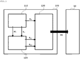
- FIG. 1 is a block diagram that shows a schematic configuration of a high-frequency power supply device according to Embodiment 1 which is a representative example of the invention.
- a high-frequency power supply device 100 includes, by way of example, a synchronous pulse generation mechanism 110 that generates a synchronous pulse P1 that includes output level information and output timing information of a high-frequency pulse PO to be output, an output level setting mechanism 120 that generates output level signals S L1 , S L2 for setting output levels of the high-frequency pulse PO based on the output level information of the synchronous pulse P1, and an oscillation mechanism 130 that receives a period reference signal S s based on the output timing information of the synchronous pulse P1 and the above-mentioned output level signals S L1 , S L2 to thereby oscillate the high-frequency pulse PO.
- the high-frequency pulse PO output from the high-frequency power supply device 100 is fed to a target device 10, such as plasma or laser generation device, induction heating device, ultra
- FIG. 2 is a block diagram showing an example of a specific configuration of the synchronous pulse generation mechanism according to Embodiment 1.
- the synchronous pulse generation mechanism 110 of Embodiment 1 includes a synchronous pulse formation circuit 112 that forms the above-mentioned synchronous pulse P1, a period reference signal generation unit 114 that generates the period reference signal S s at a period reference time in the synchronous pulse P1, and a clocking mechanism 116 that clocks an output stop time based on the period reference signal S s to send out an output stop signal S T to the output level setting mechanism 120.
- the synchronous pulse P1 output from the synchronous pulse formation circuit 112 is also fed to the output level setting mechanism 120, about which will be described later.
- the synchronous pulse formation circuit 112 includes output level information (amplitude value) and output timing information (amplitude changing timing), by way of example, and outputs an approximately rectangular periodic pulse waveform that defines two output levels L1, L2 on a vertical axis with respect to an elapsed time on a horizontal axis.
- FIG. 2 illustrates the case where the output levels are the high level L1 and the low level L2, the pulse waveform may have three or more output levels as long as the waveform is an approximately rectangular periodic wave.
- the synchronous pulse P1 is not limited to the rectangular wave, and may include any waveform that contains the output level information and the output timing information, such as sine wave or extremely-short pulse. Furthermore, the synchronous pulse P1 may consist of a plurality of signal waveforms. For example, there is a technique for performing AND operation on a plurality of signal waveforms to obtain an output level and output timing.
- the period reference signal generation unit 114 uses the synchronous pulse P1 received from the synchronous pulse formation circuit 112 to identify the output timing information which is a time reference of a period as one of the features of this synchronous pulse P1, and outputs the period reference signal S s at the identified timing.
- the time reference of the period is a time of switching from the low level L2 to the high level L1 (rising time), by way of example.
- the number of the period reference signals S s is not limited to one in one period, and for example, a time of switching from the high level L1 to the low level L2 (falling time) may be employed, in addition to the above-mentioned rising time from the low level L2 to the high level L1.
- the clocking mechanism 116 is configured, by way of example, to receive the period reference signal S s from the period reference signal generation unit 114, and then continue to send out an output stop signal S T to the output level setting mechanism 120, which will be described later, from the time of receiving the period reference signal until after a lapse of a predetermined output stop time.
- the clocking mechanism 116 is configured such that any timing can be selected for the predetermined output stop time with respect to a clock period of a clock pulse generator 132, which will be described later (see FIG. 4 ). This enables to arbitrarily select timing when the sending of the output stop signal S T is stopped.
- FIG. 3 is a block diagram showing an example of a specific configuration of the output level setting mechanism according to Embodiment 1.
- the output level setting mechanism 120 of Embodiment 1 includes a level determination unit 122 for issuing a first level setting command S 1 or second level setting command S 2 in accordance with an amplitude value (output level information) of the synchronous pulse P1, and a level setting signal generation unit 124 for generating level setting signals (first level setting signal S L1 and second level setting signal S L2 ) in response to the output stop signal S T as well as the first level setting command S 1 and the second level setting command S 2 .
- the level setting signal generation unit 124 includes a first level setting signal generator 126 for generating the first level setting signal S L1 while the first level setting command S 1 is being received, and a second level setting signal generator 128 for generating the second level setting signal S L2 while the second level setting command S 2 is being received.
- the level determination unit 122 is configured to receive the synchronous pulse P1 from the synchronous pulse formation circuit 112, and send out a predetermined setting command in real time according to the output level of the received synchronous pulse P1. For example, the level determination unit 122 in Embodiment 1 sends out the first level setting command S 1 while the synchronous pulse P1 is at the high level L1, and when the level of the synchronous pulse P1 is changed to the low level L2, sends out the second level setting command S 2 .
- the first level setting signal generator 126 generates the first level setting signal S L1 in response to the first level setting command Si received from the level determination unit 122.
- the second level setting signal generator 128 generates the second level setting signal S L2 in response to the second level setting command S 2 received from the level determination unit 122.
- the level setting signal generation unit 124 is configured not to output the first level setting signal S L1 generated by the first level setting signal generator 126 or the second level setting signal S L2 generated by the second level setting signal generator 128 to the oscillation mechanism 130 while receiving the output stop signal S T from the synchronous pulse generation mechanism 110.
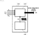
- FIG. 4 is a block diagram showing an example of a specific configuration of the oscillation mechanism according to Embodiment 1.
- the oscillation mechanism 130 includes a clock pulse generator 132 for generating a clock pulse P2 in a predetermined high frequency range, and an oscillation amplifier 134 for receiving the period reference signal S s from the synchronous pulse generation mechanism 110, the first level setting signal S L1 and the second level setting signal S L2 from the output level setting mechanism 120, and the above-mentioned clock pulse P2, so as to form a high-frequency pulse PO based on these signals.
- the clock pulse generator 132 is for generating the clock pulse P2 at high frequency (several hundreds of kHz to several tens of MHz) according to the output of the high-frequency pulse PO, e.g., generating the clock pulse P2 of 13.56 MHz. Moreover, in addition to generating the above-described clock pulse P2 at a certain high frequency at regular intervals, the clock pulse generator 132 has another function of resetting timing of the generation of the clock pulse P2 (set to a desired phase) at a desired time t rst (see FIG. 5 or 6 ).
- the oscillation amplifier 134 determines oscillation timing for the high-frequency pulse PO based on the period reference signal S s , and amplifies the amplitude value of the clock pulse P2 based on the first level setting signal S L1 and the second level setting signal S L2 to generate the high-frequency pulse PO.
- FIG. 5 is a graph showing an example of an output waveform that can be obtained by an output control method for the high-frequency power supply device according to Embodiment 1.
- the synchronous pulse P1 formed by the synchronous pulse formation circuit 112 in the synchronous pulse generation mechanism 110 is formed as a periodic pulse signal that will be at the high level L1 at an interval of a time T L1 and at the low level L2 at an interval of a time T L2 .
- a rising time to the high level L1 which is a time reference of one pulse period, is derived from the concerned synchronous pulse P1, and the period reference signal generation unit 114 sends out the period reference signal S s at each rising time, by way of example.
- the synchronous pulse P1 is also fed to the output level setting mechanism 120, and the level determination unit 122 in the output level setting mechanism 120 sets an output level for each time, so that the first level setting signal generator 126 or the second level setting signal generator 128 sends out the first level setting signal S L1 or the second level setting signal S L2 to the oscillation mechanism 130. That is to say, by referring to FIG. 5(a) , the first level setting signal S L1 is sent out at the interval of the time T L1 and the second level setting signal S L2 is sent out at the interval of the time T L2 .
- the oscillation amplifier 134 in the oscillation mechanism 130 amplifies an amplitude value of the clock pulse P2 in accordance with the received first level setting signal S L1 or second level setting signal S L2 . More specifically, when the first level setting signals S L1 are received repeatedly, consecutive pulses having average height of the clock pulse P2 at the high level L1 are output as shown in FIG. 5(b) . When the second level setting signals S L2 are received repeatedly, consecutive pulses having average height of the clock pulse P2 at the low level L2 are output as shown in FIG. 5(c) .
- the output level setting mechanism 120 is configured not to send out the first level setting signal S L1 while the output stop signal S T is being received, the continuous pulses at the high level L1 are not output from the start of the interval of the time T L1 until after a lapse of the output stop time T st .
- the timing of the reset time t rst is defined in accordance with a phase ⁇ st of the high-frequency pulse PO that is firstly output after the expiration of the output stop time T st . More specifically, a phase of the clock pulse P2 is reset at the reset time t rst , so that the phase of the high-frequency pulse PO after the lapse of the output stop time T st will be the same phase at all times.
- FIG. 6 is a graph showing a variation of an output waveform obtained by the output control method for the high-frequency power supply device according to Embodiment 1.
- a rising time to the high level L1 which is a time reference of one pulse period
- the period reference signal generation unit 114 sends out a period reference signal S s at each rising time, as with the case shown in FIG. 5 .
- the output level setting mechanism 120 sends out a first level setting signal S L1 at an interval of a time T L1 and a second level setting signal S L2 at an interval of a time T L2 to the oscillation mechanism 130.
- the oscillation amplifier 134 in the oscillation mechanism 130 amplifies an amplitude value of a clock pulse P2 in accordance with the received first level setting signal S L1 or second level setting signal S L2 . Then, consecutive pulses having average height of the clock pulse P2 at the high level L1 as shown in FIG. 6(b) and consecutive pulses having average height of a clock pulse P2 at a low level L2 as shown in FIG. 6(c) are output.
- the clock pulse P2 formed by the clock pulse generator 132 is reset at an arbitrary time t rst during the output stop time T st (the arbitrary time is defined as "reset time t rst ").
- the output level setting mechanism 120 is configured not to send out the first level setting signal S L1 while receiving the output stop signal S T , when this operation is performed continuously over time from the generation of the synchronous pulse P1, the outputting of a high-frequency pulse PO is started at a time of receiving the period reference signal S s by the oscillation mechanism 130, and thereby the continuous pulses at the high level L1 are output at the interval of time T L1 , as shown in FIG. 6(e) .
- the continuous pulses at the low level L2 are output at the interval of the time T L2 .
- timing of the reset time t rst is set such that a phase ⁇ st of the high-frequency pulse PO, which is the first to be output after a lapse of the output stop time T st , is zero at all times.
- the reset of the phase of the clock pulse P2 at the reset time t rst enables to stably output the high-frequency pulse PO after the lapse of the output stop time T st such that the phase of the pulse PO is zero at all times, and yet at the same time, the outputting of the pulse PO delays by a waiting time ⁇ for matching output phases to be zero, as shown in FIG. 6(e) .
- the high-frequency power supply device and the output control method therefor are adapted to receive the period reference signal S S based on the synchronous pulse P1, the first level setting signal S L1 , the second level setting signal S L2 and the clock pulse P2, and when forming the high-frequency pulse PO based on these signals, set the output stop time T s clocked based on the period reference signal S s to be integral multiple of the clock period of the clock pulse P2, and thereby the output level setting mechanism stops sending out the first level setting signal S L1 or second level setting signal S L2 while the output stop signal S T is being received, so that the phases of the output high-frequency pulse can be matched on all occasions even if the synchronous pulse and the clock pulse are generated separately.
- FIG. 7 is a block diagram showing a schematic configuration of a high-frequency power supply device according to Embodiment 2.
- constituent elements of a high-frequency power supply device 200 according to Embodiment 2 that are the same as or similar to those of Embodiment 1 will be denoted by the same reference numerals in Embodiment 1, and the descriptions about them will not be repeated.
- the high-frequency power supply device 200 includes a synchronous pulse generation mechanism 110, an output level setting mechanism 120 and an oscillation mechanism 130.
- the high-frequency power supply device 200 of Embodiment 2 differs from the high-frequency power supply device 100 of Embodiment 1 in that the output level setting mechanism 120 sends out a level-zero signal S L0 to the oscillation mechanism 130.
- FIG. 8 is a block diagram showing an example of a specific configuration of the output level setting mechanism according to Embodiment 2.
- the output level setting mechanism 120 according to Embodiment 2 includes a level determination unit 122 that receives an output stop signal S T and a synchronous pulse P1, and issues a first level setting command S 1 or second level setting command S 2 in accordance with an amplitude value (output level) of the synchronous pulse P1, and a level setting signal generation unit 124 that generates level setting signals (level-zero signal S L0 , first level setting signal S L1 and second level setting signal S L2 ) in response to the output stop signal S T as well as the first level setting command S 1 and the second level setting command S 2 .
- level determination unit 122 that receives an output stop signal S T and a synchronous pulse P1, and issues a first level setting command S 1 or second level setting command S 2 in accordance with an amplitude value (output level) of the synchronous pulse P1, and a level setting signal generation unit 124 that generate
- the level setting signal generation unit 124 includes a level-zero signal generator 223 that generates the level-zero signal S L0 based on the output stop signal S T , and a first level setting signal generator 126 and a second level setting signal generator 128, which are similar to those of Embodiment 1.
- the level determination unit 122 is configured, as with the case of Embodiment 1, to receive the synchronous pulse P1 from the synchronous pulse formation circuit 112, and according to the output level of the synchronous pulse P1, send out the first level setting command S 1 while the synchronous pulse P1 is at a high level L1 and send out the second level setting command S 2 when the level of the synchronous pulse P1 is changed to a low level L2.
- the level-zero signal generator 223 is configured to be activated while the level setting signal generation unit 124 is receiving the output stop signal S T , and send out the level-zero signal S L0 that makes an amplitude value of a high-frequency pulse PO to be zero while the output stop signal S T is being received.
- the first level setting signal generator 126 and the second level setting signal generator 128 are configured, as with the case of Embodiment 1, to receive the first level setting command S 1 or second level setting command S 2 from the level determination unit 122 to thereby send out the first level setting signal S L1 or second level setting signal S L2 to the oscillation mechanism 130.
- the level setting signal generation unit 124 outputs only the level-zero signal S L0 to the oscillation mechanism 130 and does not output the first level setting signal S L1 or second level setting signal S L2 while receiving the output stop signal S T from the synchronous pulse generation mechanism 110.
- FIG. 9 is a block diagram showing an example of a specific configuration of the oscillation mechanism according to Embodiment 2.
- the oscillation mechanism 130 of Embodiment 2 includes a clock pulse generator 132, and an oscillation amplifier 234 that receives a period reference signal S s from the synchronous pulse generation mechanism 110, the level-zero signal S L0 , the first level setting signal S L1 and the second level setting signal S L2 from the output level setting mechanism 120, and the clock pulse P2, so as to form a high-frequency pulse PO based on these signals.
- FIG. 10 is a graph showing an example of an output waveform obtained by the high-frequency power supply device and an output control method therefor according to Embodiment 2.
- the output control method for the high-frequency power supply device according to Embodiment 2 the relationship between a synchronous pulse P1 and an output stop signal S T shown in FIGS. 10(a) to 10(d) and amplification of amplitude values with respect to a high level L1 and a low level L2 of a high-frequency pulse PO is the same as the relationship in Embodiment 1, and thus a description about it will not be repeated in here.
- the output level setting mechanism controls the outputting of the level-zero signal Z L0 for making the output level to be zero to the oscillation mechanism while the output stop signal S T is being output, thereby enabling to perform the control such that even if a dummy bounce pulse (damping pulse P D ) is produced due to the switching of the output level at an end of an output interval (time T L2 ) of a last high-frequency pulse PO, an erroneous pulse output is prevented by making an amplitude value in an actual output to be zero, as shown in FIG. 9(e).
- Embodiments 1 and 2 illustrate that the output stop time T st is set at the early outputting stages at the high level L1.
- the output stop time T st can be set at the early outputting stages at the low level L2, or at the early outputting stages at the high level L1 and the low level L2. This makes it possible to control the wave number to be kept at a constant value for each period during outputting the high-frequency pulse PO.
- Embodiments 1 and 2 may not be separate constitutions of the invention, and may be applied as one high-frequency power supply device by combining their respective features.
Landscapes
- Physics & Mathematics (AREA)
- Engineering & Computer Science (AREA)
- Plasma & Fusion (AREA)
- Chemical & Material Sciences (AREA)
- Analytical Chemistry (AREA)
- Plasma Technology (AREA)
- Drying Of Semiconductors (AREA)
Applications Claiming Priority (2)
| Application Number | Priority Date | Filing Date | Title |
|---|---|---|---|
| JP2020045557A JP7383533B2 (ja) | 2020-03-16 | 2020-03-16 | 高周波電源装置及びその出力制御方法 |
| PCT/JP2021/008459 WO2021187137A1 (ja) | 2020-03-16 | 2021-03-04 | 高周波電源装置及びその出力制御方法 |
Publications (2)
| Publication Number | Publication Date |
|---|---|
| EP4124181A1 true EP4124181A1 (de) | 2023-01-25 |
| EP4124181A4 EP4124181A4 (de) | 2024-03-27 |
Family
ID=77772045
Family Applications (1)
| Application Number | Title | Priority Date | Filing Date |
|---|---|---|---|
| EP21771286.8A Pending EP4124181A4 (de) | 2020-03-16 | 2021-03-04 | Hochfrequenz-leistungsversorgungsvorrichtung und ausgangssteuerungsverfahren dafür |
Country Status (7)
| Country | Link |
|---|---|
| US (1) | US12014899B2 (de) |
| EP (1) | EP4124181A4 (de) |
| JP (1) | JP7383533B2 (de) |
| KR (1) | KR102873346B1 (de) |
| CN (1) | CN115316047B (de) |
| TW (1) | TWI848209B (de) |
| WO (1) | WO2021187137A1 (de) |
Families Citing this family (2)
| Publication number | Priority date | Publication date | Assignee | Title |
|---|---|---|---|---|
| CN113459971B (zh) * | 2021-06-27 | 2023-10-03 | 深圳新联胜光电科技有限公司 | 一种车辆行驶数据采集方法及系统 |
| JP7418389B2 (ja) * | 2021-12-28 | 2024-01-19 | 株式会社京三製作所 | 高周波電源 |
Family Cites Families (19)
| Publication number | Priority date | Publication date | Assignee | Title |
|---|---|---|---|---|
| JPH11214363A (ja) | 1998-01-23 | 1999-08-06 | Hitachi Ltd | 半導体製造方法とその装置、並びに半導体素子 |
| CN1307407A (zh) * | 2000-01-21 | 2001-08-08 | 周振权 | 一种用电力线传送脉冲信号的方法 |
| JP3660636B2 (ja) * | 2002-03-05 | 2005-06-15 | 株式会社日立ハイテクノロジーズ | プラズマ生成装置用高周波電源装置 |
| JP2005045019A (ja) * | 2003-07-22 | 2005-02-17 | Orc Mfg Co Ltd | Qスイッチレーザ装置 |
| US7190119B2 (en) | 2003-11-07 | 2007-03-13 | Lam Research Corporation | Methods and apparatus for optimizing a substrate in a plasma processing system |
| JP4879548B2 (ja) * | 2005-09-30 | 2012-02-22 | 株式会社ダイヘン | 高周波電源装置 |
| JP4963023B2 (ja) * | 2006-01-11 | 2012-06-27 | 株式会社アルバック | スパッタリング方法及びスパッタリング装置 |
| JP5319150B2 (ja) * | 2008-03-31 | 2013-10-16 | 東京エレクトロン株式会社 | プラズマ処理装置及びプラズマ処理方法及びコンピュータ読み取り可能な記憶媒体 |
| JP2010238881A (ja) * | 2009-03-31 | 2010-10-21 | Tokyo Electron Ltd | プラズマ処理装置及びプラズマ処理方法 |
| JP2011029069A (ja) * | 2009-07-28 | 2011-02-10 | Mitsubishi Electric Corp | プラズマ処理装置および半導体膜の製造方法 |
| JP5485053B2 (ja) * | 2010-07-14 | 2014-05-07 | 新電元工業株式会社 | 半導体装置、点弧角変換回路、電源装置、照明装置および信号変換方法 |
| JP5808012B2 (ja) * | 2011-12-27 | 2015-11-10 | 東京エレクトロン株式会社 | プラズマ処理装置 |
| US9462672B2 (en) * | 2012-02-22 | 2016-10-04 | Lam Research Corporation | Adjustment of power and frequency based on three or more states |
| JP6374647B2 (ja) * | 2013-11-05 | 2018-08-15 | 東京エレクトロン株式会社 | プラズマ処理装置 |
| DE102013226511B4 (de) | 2013-12-18 | 2016-12-15 | TRUMPF Hüttinger GmbH + Co. KG | Leistungsversorgungssystem und Verfahren zur Erzeugung einer Leistung |
| US10115567B2 (en) * | 2014-09-17 | 2018-10-30 | Tokyo Electron Limited | Plasma processing apparatus |
| JP6512962B2 (ja) * | 2014-09-17 | 2019-05-15 | 東京エレクトロン株式会社 | プラズマ処理装置 |
| JP7175239B2 (ja) * | 2018-06-22 | 2022-11-18 | 東京エレクトロン株式会社 | 制御方法、プラズマ処理装置、プログラム及び記憶媒体 |
| JP7262375B2 (ja) * | 2019-11-26 | 2023-04-21 | 東京エレクトロン株式会社 | プラズマ処理方法及びプラズマ処理装置 |
-
2020
- 2020-03-16 JP JP2020045557A patent/JP7383533B2/ja active Active
-
2021
- 2021-03-03 TW TW110107467A patent/TWI848209B/zh active
- 2021-03-04 WO PCT/JP2021/008459 patent/WO2021187137A1/ja not_active Ceased
- 2021-03-04 EP EP21771286.8A patent/EP4124181A4/de active Pending
- 2021-03-04 CN CN202180021281.7A patent/CN115316047B/zh active Active
- 2021-03-04 KR KR1020227034825A patent/KR102873346B1/ko active Active
- 2021-03-04 US US17/911,174 patent/US12014899B2/en active Active
Also Published As
| Publication number | Publication date |
|---|---|
| CN115316047A (zh) | 2022-11-08 |
| TW202141587A (zh) | 2021-11-01 |
| JP7383533B2 (ja) | 2023-11-20 |
| TWI848209B (zh) | 2024-07-11 |
| WO2021187137A1 (ja) | 2021-09-23 |
| EP4124181A4 (de) | 2024-03-27 |
| JP2021150031A (ja) | 2021-09-27 |
| KR102873346B1 (ko) | 2025-10-20 |
| KR20220154147A (ko) | 2022-11-21 |
| CN115316047B (zh) | 2026-03-27 |
| US20230124064A1 (en) | 2023-04-20 |
| US12014899B2 (en) | 2024-06-18 |
Similar Documents
| Publication | Publication Date | Title |
|---|---|---|
| JP7155354B2 (ja) | プラズマ処理装置、プロセッサ、制御方法、非一時的コンピュータ可読記録媒体及びプログラム | |
| KR102467354B1 (ko) | 가변 주파수 생성기들을 사용하는 스마트 rf 펄싱 튜닝 | |
| KR20210040161A (ko) | 승수 모드에 따른 무선 주파수(rf) 펄싱 임피던스 튜닝 | |
| KR101787501B1 (ko) | Rf 발생기들의 바이모달 자동 전력 및 주파수 동조의 시스템 및 방법 | |
| KR101769073B1 (ko) | 플라즈마 처리 장치 | |
| US12014899B2 (en) | High-frequency power supply device and output control method therefor | |
| CN115280903B (zh) | 高频电源装置及其输出控制方法 | |
| JP2003505868A (ja) | 誘導結合されたプラズマを用いて基板をエッチングするための装置および方法 | |
| JP2008117777A (ja) | 少なくとも2つの高周波電力発生器のドライブ制御方法、高周波電力発生器ドライブ制御装置および高周波プラズマ励起装置 | |
| TW202341223A (zh) | 在電漿處理期間用於傳送複數個波形訊號之設備與方法 | |
| TW201526099A (zh) | 電漿處理裝置及電漿處理方法 | |
| CN115280904A (zh) | 用于线性加速器与具有线性加速器的离子植入机的控制器以及控制技术 | |
| US7554414B2 (en) | Fast starting circuit for crystal oscillators | |
| JPWO2005109019A1 (ja) | タイミング発生器及び半導体試験装置 | |
| WO1997027494A1 (en) | Delay time measuring method and pulse generator for measuring delay time for use in said measuring method | |
| KR102811324B1 (ko) | 파워 동기 제어 기능이 구비된 플라즈마 제너레이터 | |
| KR102690334B1 (ko) | 플라즈마 생성 디바이스 | |
| JPH06168799A (ja) | タイミング制御装置 | |
| JPH0628244B2 (ja) | レーザ増幅器装置の励起制御装置 | |
| JPH07183227A (ja) | プラズマcvd法及びプラズマcvd装置 |
Legal Events
| Date | Code | Title | Description |
|---|---|---|---|
| STAA | Information on the status of an ep patent application or granted ep patent |
Free format text: STATUS: THE INTERNATIONAL PUBLICATION HAS BEEN MADE |
|
| PUAI | Public reference made under article 153(3) epc to a published international application that has entered the european phase |
Free format text: ORIGINAL CODE: 0009012 |
|
| STAA | Information on the status of an ep patent application or granted ep patent |
Free format text: STATUS: REQUEST FOR EXAMINATION WAS MADE |
|
| 17P | Request for examination filed |
Effective date: 20220908 |
|
| AK | Designated contracting states |
Kind code of ref document: A1 Designated state(s): AL AT BE BG CH CY CZ DE DK EE ES FI FR GB GR HR HU IE IS IT LI LT LU LV MC MK MT NL NO PL PT RO RS SE SI SK SM TR |
|
| DAV | Request for validation of the european patent (deleted) | ||
| DAX | Request for extension of the european patent (deleted) | ||
| A4 | Supplementary search report drawn up and despatched |
Effective date: 20240227 |
|
| RIC1 | Information provided on ipc code assigned before grant |
Ipc: H01J 37/32 20060101ALI20240221BHEP Ipc: H05H 1/46 20060101AFI20240221BHEP |